CRKITS CRK-10 CW User manual
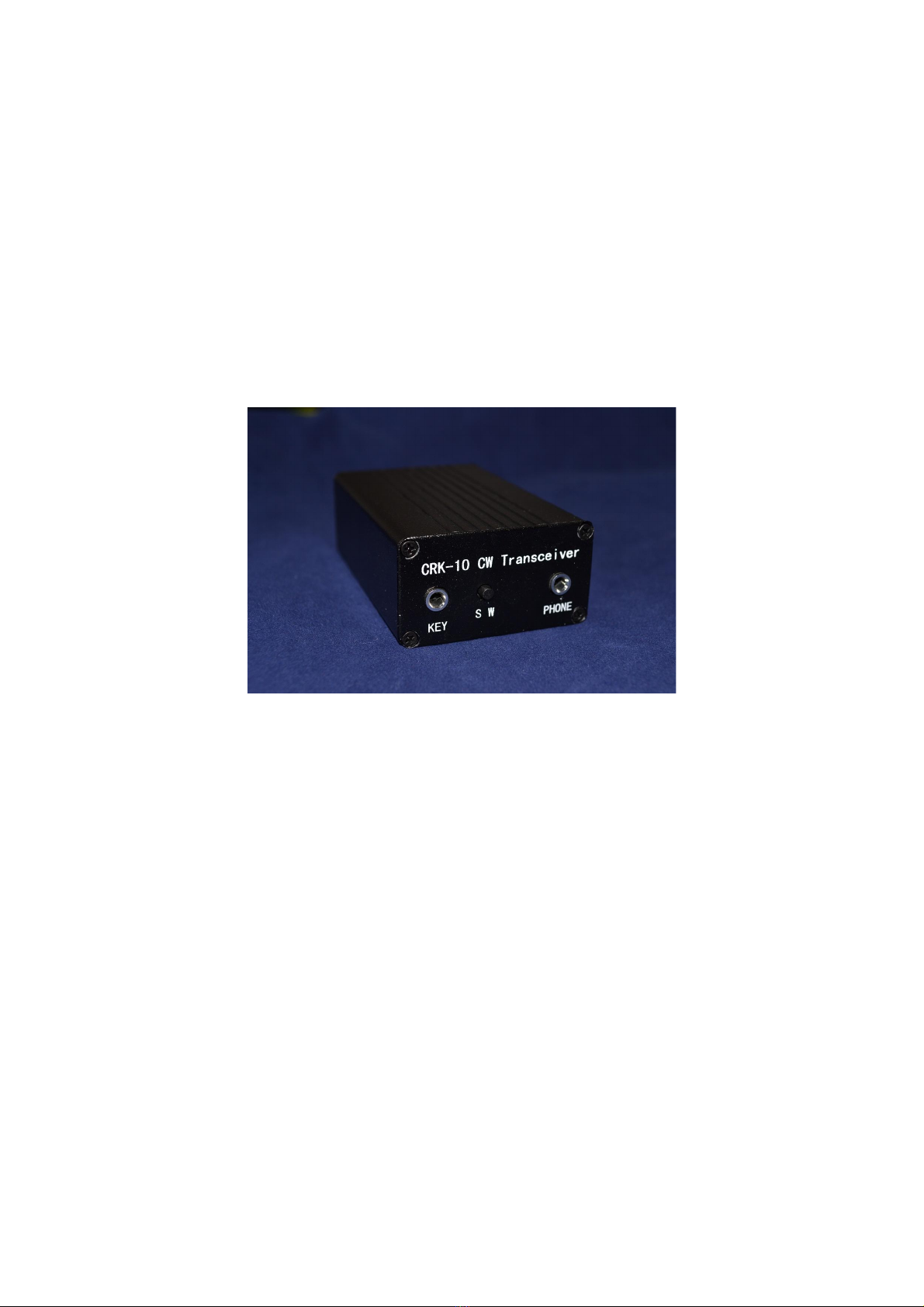
CRK-10 CW Transceiver Kit Manual
Rev. B
CRKITS.COM
Oct 22, 2012
RockMite was intro uce to China years ago by BD6CR/4. BD4RG, the esigner of HB-1A an
HB-1B, improve the esign by rewriting the firmware, increasing RF power output, an
smoothing the keying. The improve version is calle Octopus in China, an alrea y receive goo
reputation an popularity among Chinese QRPers. Now CRKITS.COM prou ly intro uces this kit
to the worl wi e, an names it as CRK-10 CW Transceiver kit.
The RF output power is about 3 watt at 12V. Power supply range is 9-15V. TX current is about 500
mA, an RX current is about 15 mA (measure at 12V). The built-in MCU can generate si e tone of
about 700 Hz, switch RX/TX, an act as a keyer for not only pa le (normal pa le or bug key
simulation mo e), but also straight key.
The receiver is a irect conversion receiver, but the sensitivity is very high because of a two-pole
crystal filter in the receiver front-en an an au io filter, which block interference an filter out
backgroun noise. The MCU automatically shifts TX frequency, generates si e tone an acts as the
keyer, which makes the whole ra io quite practical. The power supply polarity protection an the
high SWR protection make the ra io urable.
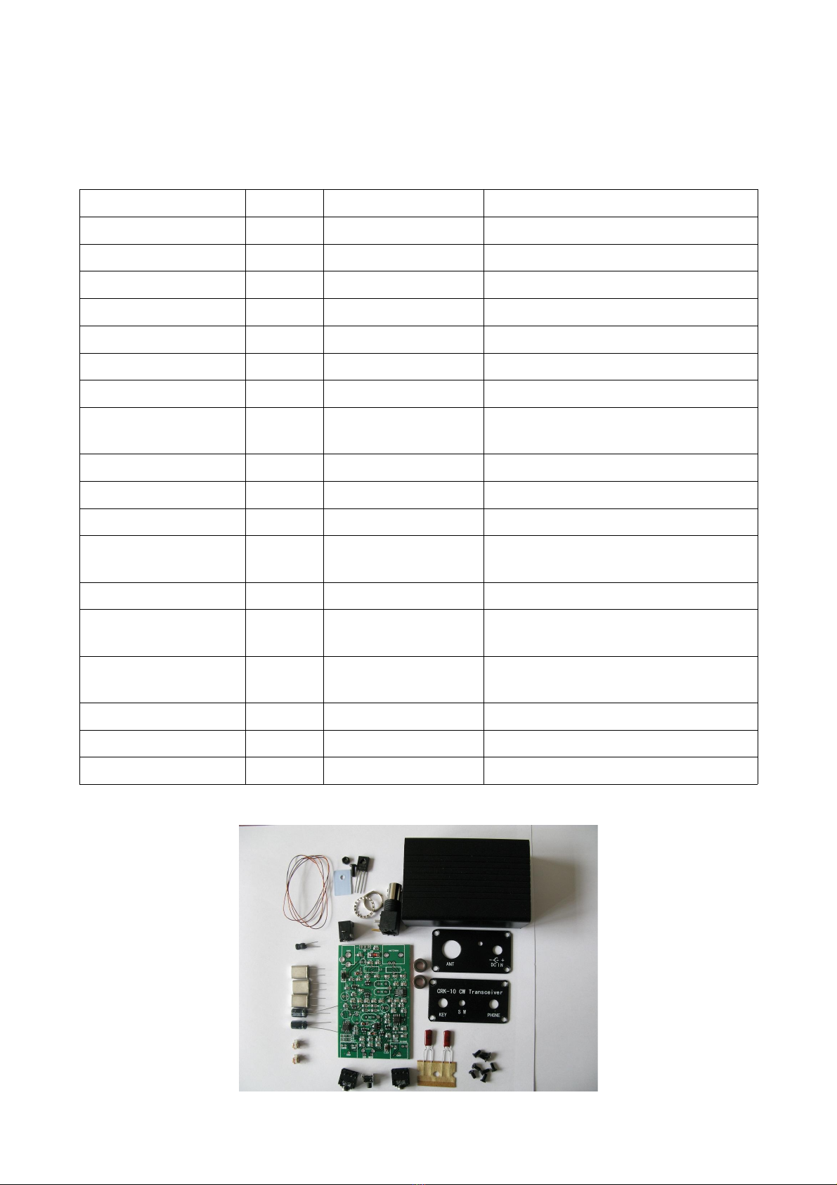
Parts Inventory
Most of the components of this kit are SMD parts an alrea y pre-mounte by factory on PCB, so
you will only nee to sol er about 20 through-hole parts inclu ing all the connectors an buttons.
Part list is shown below.
Item Quantity Value Comments
Custom case 1 CRK-10, black With front an rear panels
PCB assembly 1 CW-DC-1N All SMD parts pre-mounte
In uctor, fixe 1 10uH, black L1
In uctor, toroi 2 T37-2, re L2 (10 turns), L3 (12 turns)
Enamel wire 0.4m 0.38mm iameter For L2 an L3 win ing
Capacitor, trimmer 2 9-50pF C23 (for TX), C24 (for RX)
Capacitor, electrolytic 2 100uF 25V C1, C32
Capacitor, polyester
film
2 0.01uF, 103J C30, C31
Push button 1 PCB mount SW
3.5mm jack 2 3.5mm stereo type PHONE, KEY
DC IN connector 1 2.1mm type +V, 12-13.8V power supply connector
Crystal 3 7.010, 7.020, 7.025 or
7.030 MHz
X1, X2, X3
Power Amp. transistor 1 2SC1162 Q6
Thermal pa /
insulator
1 TO-220 type With back paste, stick to inner si e of
the rear panel
M3x8 screw 1 M3x8, black, pan
hea
For fixing the transistor
M3 nut 1 M3, black For fixing the transistor
Antenna connector 1 BNC, PCB mount Black, with washer an nut
Panel screw 8 Black, flat hea For front an rear panels
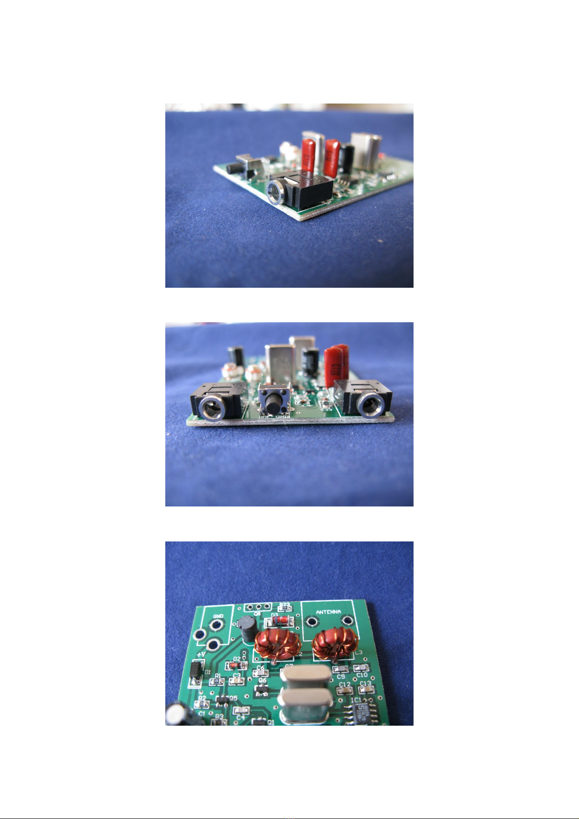
The whole kit will look like this:
Step by Step Building
It takes about an hour to buil an align the kit, so it is an i eal one-evening kit to give you some
pure fun of kit buil ing an QRP operation.
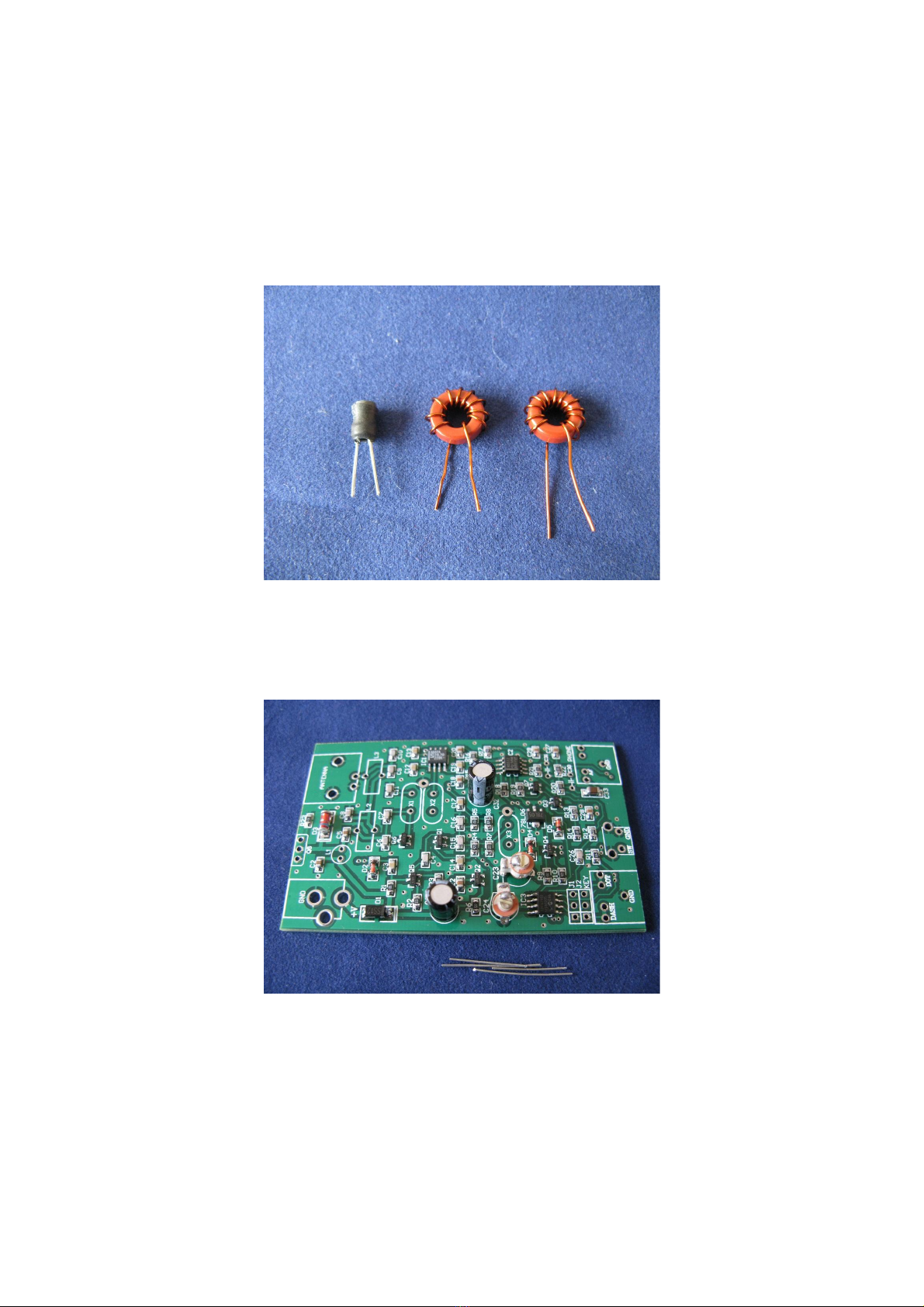
Step 1: Toroids Winding
Follow the picture to win 10 turns for L2 an 12 turns for L3. They are parts of the low-pass filter
to purify the transmitter output. Scratch the enamel of wire en ings an tin them well. L1 is also
shown in the picture. It is a factory ma e in uctor, so you on't have to win it here.
Step 2: Capacitors C23, C24, C1 and C32
Follow the picture to put C23 in place an sol er. Do the same for C24. C24 controls the receiver
frequency an C23 in parallel of C24 control the transmit frequency. Procee to C1 an C32. Check
the polarity when you sol er. Trim the lea s of C1 an C32 an reserve for use in the following
steps.

Step 3: J1 and J2 Jumpers
The J1 an J2 jumpers are use to swap ash an ot wiring. Here, we can refer to the iagram to
sol er two jumper wires. Note that straight key is only supporte in one setting (but not the one
shown in the picture below).
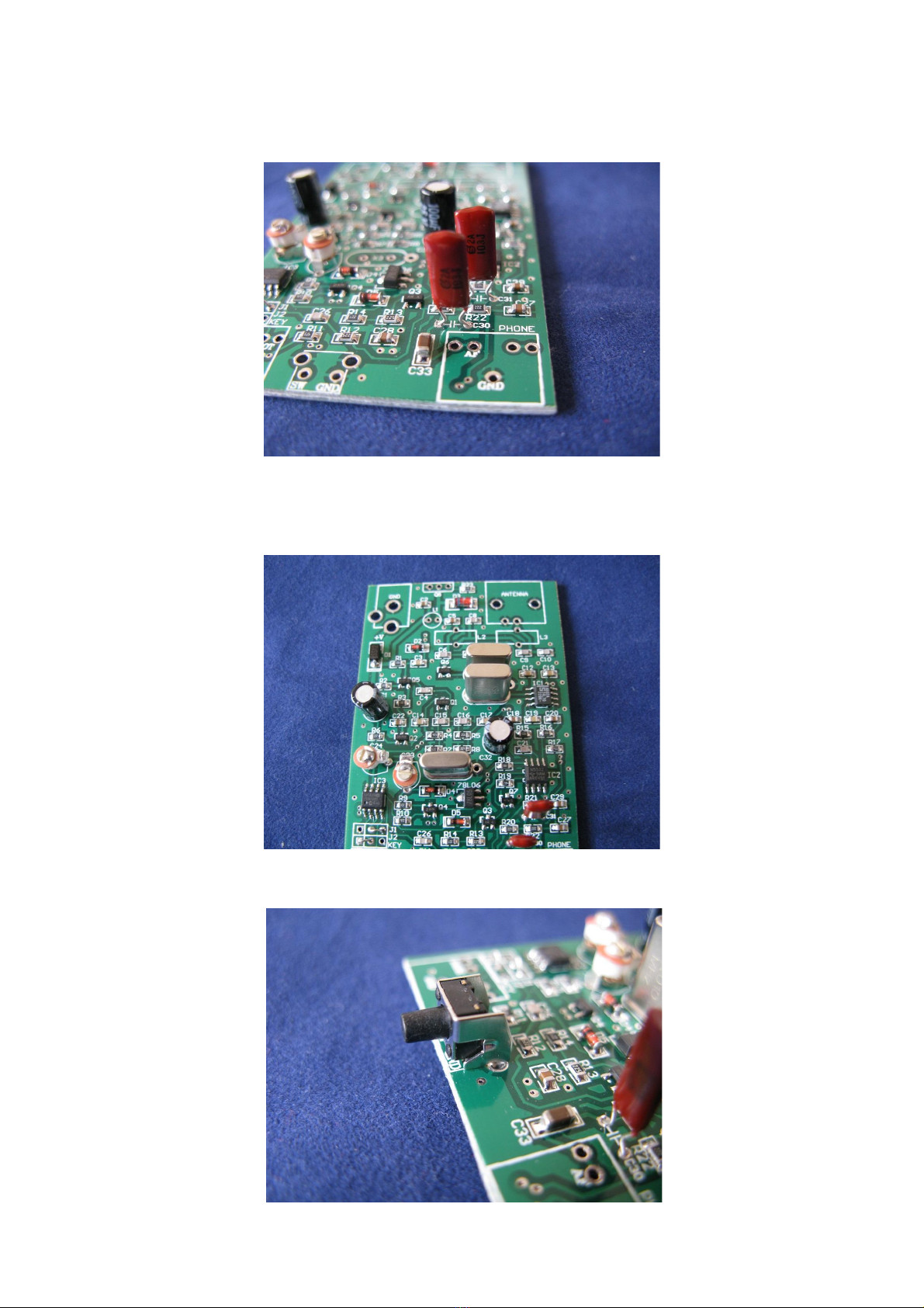
Step 4: Capacitors C30, C31
Follow the picture to sol er C30 an C31. C30 an C31 are parts of the au io filter.
Step 5: Crystals X1, X2 and X3
Follow the picture to sol er X1, X2 an X3. X1 an X2 form a 2-pole crystal filter in the front-en
of the irect conversion receiver, while X3 is working as the oscillator for both the receiver an
transmitter.
Step : Push Button SW
Follow the picture to install an sol er SW. SW is an important part of human-machine interface.
Step 7: 3.5 mm Jack PHONE
Follow the picture to install an sol er PHONE jack. Low impe ance (aroun 32 ohm) an high
sensitivity stereo hea phones are recommen e here.
Step 8: 3.5 mm Jack KEY
Follow the picture to install an sol er KEY jack. Both pa le an straight key are supporte .
Step 9: Inductor L1, L2 and L3
Follow the picture to sol er L1, L2 an L3.

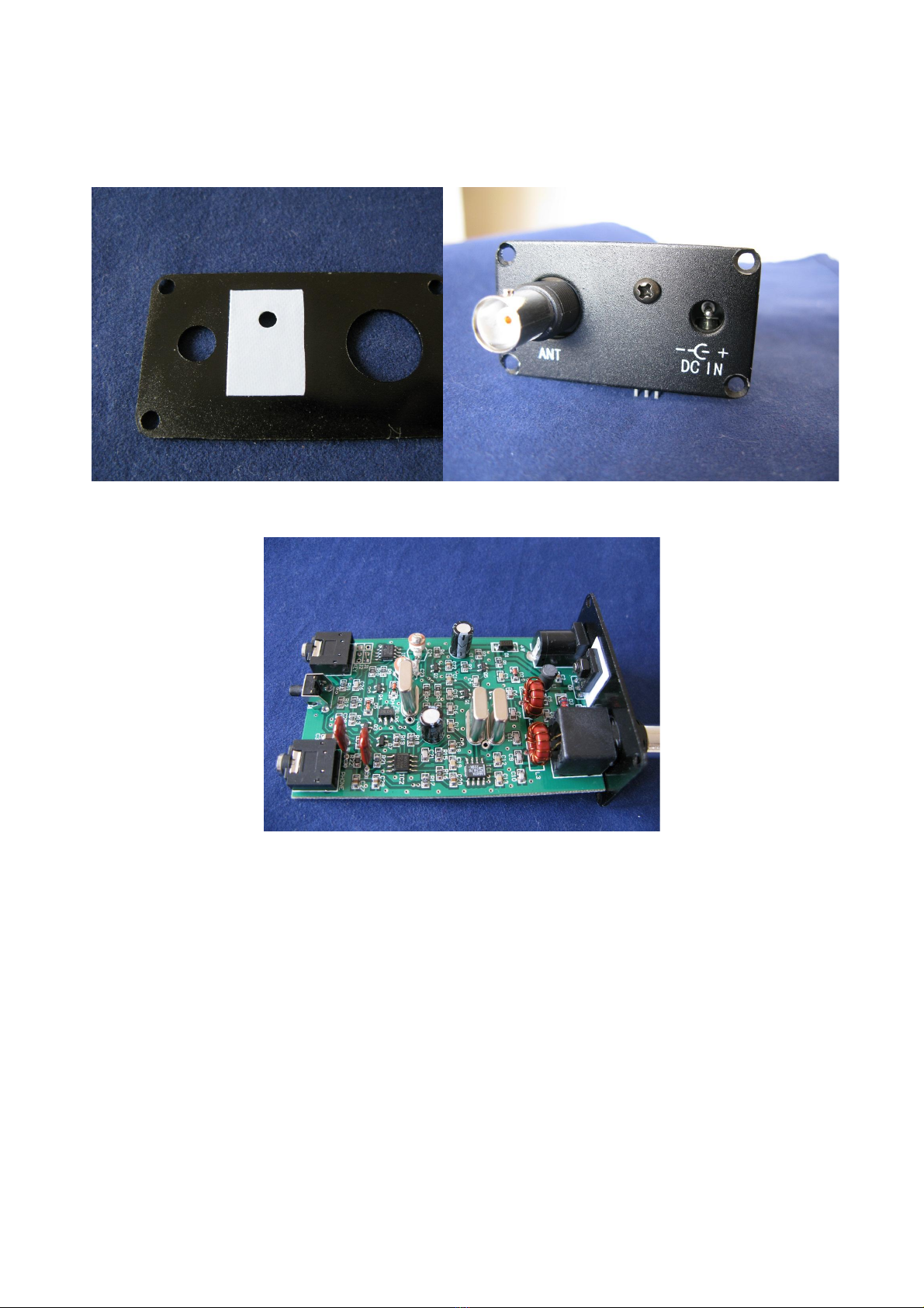
Step 10: DC IN Connector
Follow the pictures to install DC IN connector. Leave one si e pin NOT sol ere . The center or V+
marking means positive. 12~13.8V an at least 1A power supply is recommen e .
Step 11: Antenna Connector
Follow the pictures to install the BNC type antenna connector.
Step 12: Power Amplifier Transistor
Follow the pictures to install the power amplifier transistor. Keep the pin about 4 mm above the
boar , an only sol er one pin first.
Step 13: Thermal Pad / Insulator
Follow the pictures to stick the thermal pa to the inner si e of the rear panel, an fix the transistor
to the rear panel by M3 screw an nut. Make sure the DC IN connector can be plugge in when you
fasten the screw. Then sol er all the pins of the transistor an trim the lea s.
Step 14: Ready for Alignment
Follow the following alignment section to align the ra io, before final assembly.
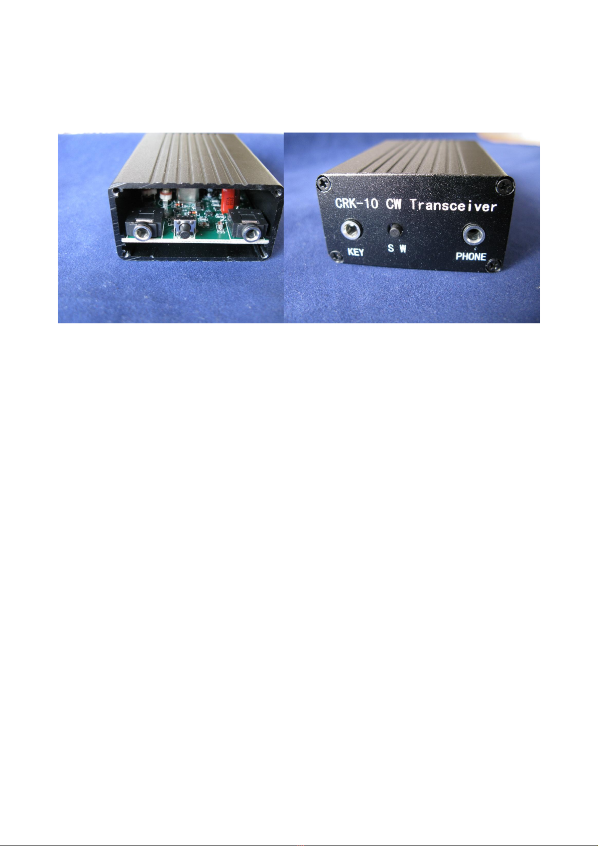
Step 15: Final Assembly
Follow the pictures to sli e the boar to the case an finish the final assembly. Fix the rear panel
an front panel by the 8 pcs flat hea panel screws. Congratulations! You are one with your
buil ing an please enjoy some QSO's now.

Operation
If an effective antenna is use , 3 watt RF power is goo enough to make others hear . Although it is
a QRP ra io, you are encourage to call CQ to be able to make more successful QSO's. Luckily you
can use the push button to automatically call CQ.
Everything else is straightforwar but the keyer operation, which will be a resse below. The
human-machine interface is ma e by the push button, a pa le an a hea phone.
All parameters will be store in the MCU, an it will not be lost after power own.
Paddle or Straight Key Keyer Mode Switch
The MCU automatically etects pa le or straight key, as long as you plug in the key before power
on. The mechanism is that the MCU etects if the ring of the 3.5 mm stereo plug (pin 3 of the
MCU) is permanently short with the shiel (groun ) or floating. For straight key, it is short. For
pa le, it is floating. If you hear Morse co e A (Automatic) after power on, it means a pa le is
etecte an it works in normal pa le mo e; Morse co e B (Bug) means a pa le is etecte an it
works in bug key simulation mo e; an Morse co e M (Manual) means a straight key is etecte
an it works in straight key mo e.
Auto CQ
Briefly press SW button an it automatically sen CQ CQ CQ DE + your call three times + K. If
you want to stop the auto CQ, press an hol SW button for 1 sec an release.
Speed Adjustment
Press SW button for more than 2 sec, you will hear Morse co e S (spee ). Release it an a just the
keying spee by pa le within 8 sec (or it automatically exits to keep the original spee ). Press ot
will increase the spee , an press ash will ecrease the spee . Briefly press SW button an you
can hear Morse co e E to confirm exit, or wait about 8 sec to automatically exit.
Call sign Input
Press SW button for about 2 sec, you will hear Morse co e S (spee ). Keep pressing for another 2
sec, you will hear Morse co e I (input). Release it an input your call sign (up to 10 character) just
like you make QSO with your pa le within 8 sec (or it automatically exits to keep the original call
sign). Briefly press SW button an you can hear Morse co e E to confirm exit, or wait about 8 sec
to automatically exit.
Paddle Mode Selection (Normal Paddle/ Bug Simulation)
Press SW button for about 2 sec, you will hear Morse co e S (spee ). Keep pressing for another 2
sec, you will hear Morse co e I (input). Keep pressing for another 2 sec, you will hear Morse co e
M (mo e). Release it an sen ot by your pa le, you will hear Morse co e NOR, an the ra io
will be chosen to work in normal pa le mo e. If you sen ash by your pa le, you will hear
Morse co e BUG, an the ra io will be chosen to work in bug simulation mo e. In bug simulation
mo e, ots will be sent automatically by the MCU an ashes will be sent manually. Note that the
keyer oes not actually support mechanical bug key.
Adding /QRP
You can choose to a /QRP or not in auto CQ. Press SW button an power on the ra io, you will
hear normal Morse co es (A or M or B) to in icate working mo e. Keep pressing SW button for 1

sec or 2, you will hear Morse co e QRP. Release it an now auto CQ will a /QRP after the thir
time of your call sign. Repeat the above operation you will hear Morse co e NO, an it means auto
CQ will not a /QRP.
Alignment
It is preferre that you have a power supply of 12~13.8V with short circuit protection. Connect the
power supply to the CRK-10 to see if it works. The overall receive current shoul be about 15 mA.
Disconnect the power supply, connect a hea phone, a pa le an an antenna or a 50 ohm ummy
loa , then connect the power supply again, you shoul hear ot ash. Touch the antenna connector
center pin with tweezers, an you shoul hear some clicks. It means the receiver works.
Now procee to TX alignment. Enter the straight key mo e an press an hol the key to see if the
overall current is about 500 mA. If it is, it means the transmitter works.
Use a commercial amateur ra io to transmit a CW tone at the specifie frequency, an a just the
capacitor trimmer C24 to make the receiver frequency exactly on the specifie frequency (the tone
from the hea phone is lou an clear, within 700~800 Hz range). A just the capacitor trimmer C23
to make the transmit frequency exactly to the specifie frequency.

Theory of Operation
The MCU servers a controller an a keyer. It controls RX/TX switch, inclu ing receiver mute an
transmit frequency shift. As a keyer, it rea s the key input, keys the transmitter to sen the signal
an generate si e tone as well.
The receiver is a typical NE602 irection conversion receiver, with the exception that it only
receives one frequency, so a 2-pole crystal filter is a e in the front-en to block most of the
broa cast interference out. The NE5532 op-amp serves as an au io filter an amplifier to rive a
hea phone. Q3 2N5485 is controlle by the MCU to mute the receiver in transmit.
The transmitter chain is simple. 2N3904 is the oscillator. C24 controls the receiver frequency an
C23 in parallel of C24 control the transmit frequency. 2N4401 is a buffer amplifier an it is also a
keying circuit. The power amplifier is 2SC1162. The LPF filters the transmit harmonic signals.
Troubleshooting
If the receive current is much higher than 15 mA, it means the circuit has issue. Inspect all the
components to make sure they are installe properly, especially the components with polarity such
as electrolytic capacitors, an IC orientation. If all the components are installe properly but the
symptom persists, most likely it is because of the PCB short. Please inspect carefully an cut the
short circuit trace by a knife.
You can also refer to the following voltage chart to help you fin the issue. If the voltages of one IC
is abnormal, normally you can check the IC itself or its peripheral components.
Reference voltage on each IC: (Power supply 12V, measured in R mode)
Pin 1 2 3 4 5 6 7 8
IC1 1.4 1.4 0 3.9 3.9 4.9 4.2 5
IC2 5 5 5 0 4.8 5 5 11.8
IC3 5 5 5 5 5 0 0 0
Table of contents
Other CRKITS Transceiver manuals


Popular Transceiver manuals by other brands


RigExpert
RigExpert WTI-1 user manual

Radio Shack
Radio Shack HTX-10 owner's manual

Vertex Standard
Vertex Standard VXA-710 SPIRIT operating manual

Alinco
Alinco DR-112E Specifications

Kenwood
Kenwood D700 Setup

Technisonic Industries Limited
Technisonic Industries Limited TSC-4400 Installation and operating instructions