CRKITS CRK-10A Manual

CRK-10A CW Transceiver
Kit Manual
Rev. A
CRKITS.COM
May 19, 2013
C ange History:
May 19, 2013: Initial release - Rev. A

Introduction
T anks for c oosing CRK-10A CW Transceiver kit. It is a great one-evening project to provide
you pure fun of bot kit building and QRP operation. CRK-10A design is inspired by RockMite
from Small Wonder Labs. RockMite was introduced to C ina years ago by BD6CR/4. BD4RG, t e
designer of HB-1A and HB-1B, improved t e design by rewriting t e firmware, increasing RF
power output, and smoot ing t e keying. T e improved version is called Octopus in C ina, and as
already received a good reputation and popularity among C inese QRPers. Previously, we
introduced t e SMD version 40 meter CW transceiver kit called CRK-10, and now we are glad to
announce t e t roug - ole version CRK-10A wit improvements.
T e major c anges from CRK-10:
•CRK-10 is a ybrid kit wit all t e SMD parts pre-mounted and about 20 pcs t roug - ole
parts to install, but CRK-10A is a pure kit wit all t roug - ole parts to install.
•CRK-10 supports 40 meter band only, w ile CRK-10A supports 40 meter or 30 meter band.
•CRK-10A removes t e paddle dot/das wiring jumpers, and adds a pus button to confirm
t e side band of t e incoming signal
•CRK-10A follows KN-Q7A style to use PCB panels, provides IC sockets and case feet to
make it a more complete and good looking kit
T e CRK-10A specifications follow CRK-10 t at t e RF output power is about 3 watt at 12V
(slig tly lower for 30 meter band). Power supply range is 9-15V. TX current is about 500 mA, and
RX current is about 15 mA (measured at 12V). T e built-in MCU can generate side tone of about
700 Hz, switc RX/TX, and act as a keyer for not only paddle (normal paddle or bug key simulation
mode), but also straig t key.
T e receiver is a direct conversion receiver, but t e sensitivity and selectivity are very ig
because of a two-pole crystal filter in t e receiver front-end and an audio filter, w ic block
interference and filter out background noise. T e MCU automatically s ifts TX frequency,
generates side tone and acts as t e keyer, w ic makes t e w ole radio quite practical. T e power
supply polarity protection and t e ig SWR protection make t e radio durable.
Disclaimer
We offer t e kit as is and do not guarantee t e assembled kit by yourself can meet your local
regulatory requirements, including spurious, environmental or ot ers. As some parts used in t e kit
are obsolete, we cannot guarantee t at all t e components in t e kit are brand new, but we bear t e
responsibility of providing t em as good as possible.
Parts Inventory
Follow t e part list below to do parts inventory first. Please note t e difference between 30
meter kit and 40 meter kit. If t ere are any missing parts or questions, please contact your local
distributor or CRKITS.COM directly by email at rongx @gmail.com.
Item Quantity Value Comments
Resistor 2 22 R3, R18
Resistor 2 100 R1, R23
Resistor 2 220 R8, R14
Resistor 2 1 k R5, R9
Resistor 2 2.2 k R6, R22
Resistor 4 4.7 k R10, R15, R16, R24
Resistor 2 22 k R7, R20
Resistor 1 33 k R2
Resistor 2 47 k R4, R11
Resistor 3 220 k R17, R19, R21
Resistor 2 2.2 M R12, R13
Capacitor, ceramic 3 33 p C7, C11, C26
Capacitor, ceramic 1 56 p (30 m) or 100 p
(40 m)
C9
Capacitor, ceramic 6 100 p C4, C15, C16, C21, C34, C35
Capacitor, ceramic 2 220 p (30m) or 470 p
(40 m)
C6, C8'
Capacitor, ceramic 2 470 p (30m) or 1000 p
(40 m)
C8, C10
Capacitor, ceramic 7 0.01 uF C3, C12~C14, C17, C19, C22
Capacitor, ceramic 1 0.01 uF (30 m) or
leave it not installed
(40 m)
C25
Capacitor, ceramic 7 0.1 uF C2, C5, C18, C20, C27~C29
Capacitor, trimmer 2 9-50 pF C23 (for TX), C24 (for RX)
Capacitor, electrolytic 1 10 uF 25 V C33
Capacitor, electrolytic 2 100 uF 25 V C1, C32
Capacitor, polyester
film
2 0.01 uF, 2A103J C30, C31
Diode 7 1N4148, glass body D2, D4, D5~D9
Diode 1 1N5817, black D1
Diode 1 1N4755A, silver D3
Regulator IC 1 78L05 78L05
IC socket 3 8-pin 8-pin

IC, balanced mixer 1 NE602 IC1
IC, op amp 1 NE5532 IC2
IC, MCU 1 12F629, programmed IC3
Transistor 2 2N3904 Q1, Q2
Transistor 1 2N3906 Q4
Transistor 1 2N4401 Q5
Field Effect Transistor 1 J309 Q3
Power Amp. transistor 1 2SC1162 Q6
Inductor, fixed 1 10 uH L1
Inductor, toroid 2 T37-2, red L2 (10 turns), L3 (12 turns)
Enamel wire 0.4m 0.38mm diameter For L2 and L3 winding
Pus button 2 PCB mount SW, SW1
3.5mm jack 2 3.5 mm stereo type PHONE, KEY
DC IN connector 1 2.1 mm type +V
Crystal 3 7.010, 7.020, 7.025,
7.030, 10.106 or
10.130 MHz
X1, X2, X3
T ermal pad /
insulator
1 TO-220 type Wit back paste, stick to inner side of
t e rear panel plated area
M3x8 screw 1 M3x8, black, pan
ead
For fixing 2SC1162
M3 nut 1 M3, black For fixing 2SC1162
Antenna connector 1 BNC, PCB mount ANTENNA, wit was er and nut
M2.5x6 panel screw 8 Black, pan ead For front and rear panels
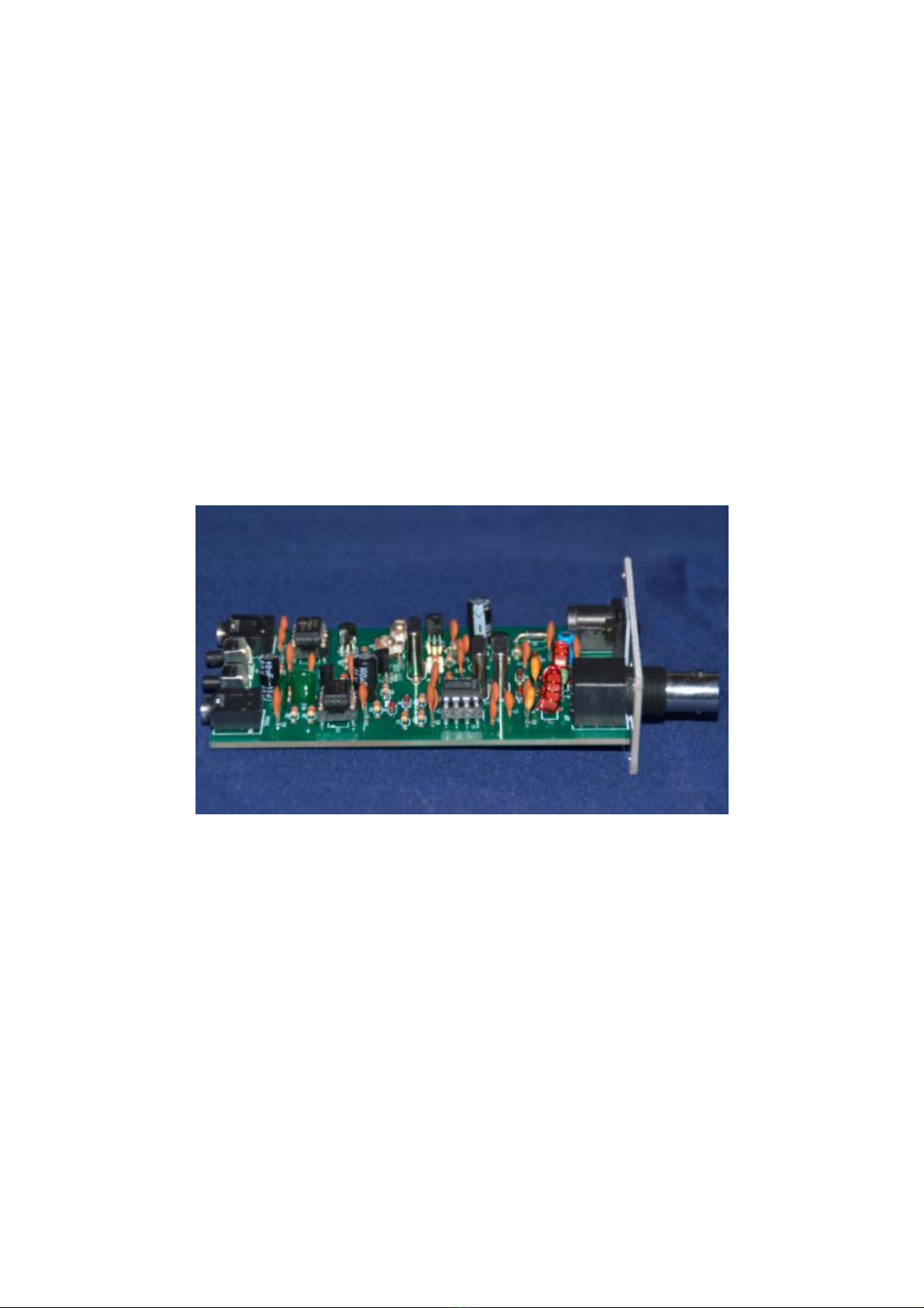
Case 1 CRK-10, black Wit front and rear panels
PCB 1 CW-DC-1P

Step by Step Building
It takes about 2.5 ours to build and align t e kit. You will need to prepare basic soldering and
alignment tools to be able to build t is kit.
Step 1: Resistors
Stuff all t e resistors, solder and cut t e extra leads. If you are not sure about t e color codes,
you can use an o m meter to verify value before you solder.
First 3 colors are listed. If necessary, use an o mmeter to verify value.
•R3, R18 22 (Red, red, black)
•R1, R23 100 (Brown, black, brown)
•R8, R14 220 (Red, red, brown)
•R5, R9 1 k (Brown, black, red)
•R6, R22 2.2 k (Red, red, red)
•R10, R15, R16, R24 4.7 k (Yellow, violet, red)
•R7, R20 22 k (Red, red, orange)
•R2 33 k (Orange, orange, orange)
•R4, R11 47 k (Yellow, violet, orange)
•R17, R19, R21 220 k (Red, red, yellow)
•R12, R13 2.2 M (Red, red, green)

Step 2: Diodes
Stuff all t e diodes. Note for t e polarity. Solder and cut t e extra leads.
•D2, D4, D5~D9 1N4148, glass body
•D1 1N5817, black
•D3 1N4755A, silver

Step 3: Ceramic capacitors, regulator IC and IC sockets
Install all t e 0.01 uF (103) and 0.1 uF (104) ceramic capacitors. C25 is only required for 30
meter kit.
•C3, C12~C14, C17, C19, C22 0.01 uF
•C25 0.01 uF (30 m)
not installed (40 m)
•C2, C5, C18, C20, C27~C29 0.1 uF
Install t e DC IN socket. If it is a bit protruding outside of t e board edge, press it towards
inside t en solder.
Install 78L05 regulator IC. Make sure t e outline is aligned.
Install 3 pcs IC sockets. Make sure t e notc es are aligned.
Test: Apply power supply of 9-15 V DC, center positive, measure 5 V at pin 8 of IC1.

Step 4: Audio filter and amplifier
Install Q3 (J309). Note for static sensitive part. Handle wit care.
Install C32 (100 uF 25 V) and C33 (10 uF 25 V). Note for polarity.
Install C30 and C31 (polyester film 0.01 uF, 2A103J).
Install C21 (100 p).
Install PHONE jack.
Insert IC2 (NE5532). Note for orientation.
Test: Apply power supply, and connector a eadp one to PHONE jack. Use tweezers to touc
pin 4 of IC1 and ear noise.

Step 5: CU
Install KEY jack
Install SW
Install C26 (33 p), C34 (100 p) and C35 (100 p)
Insert IC3 (12F629). Note for orientation.
Test: Apply power supply, and connect a eadp one to PHONE jack. Press SW1 to ear Morse
code. Connect a paddle to KEY jack, send a few codes and monitor t e side tone from eadp one.
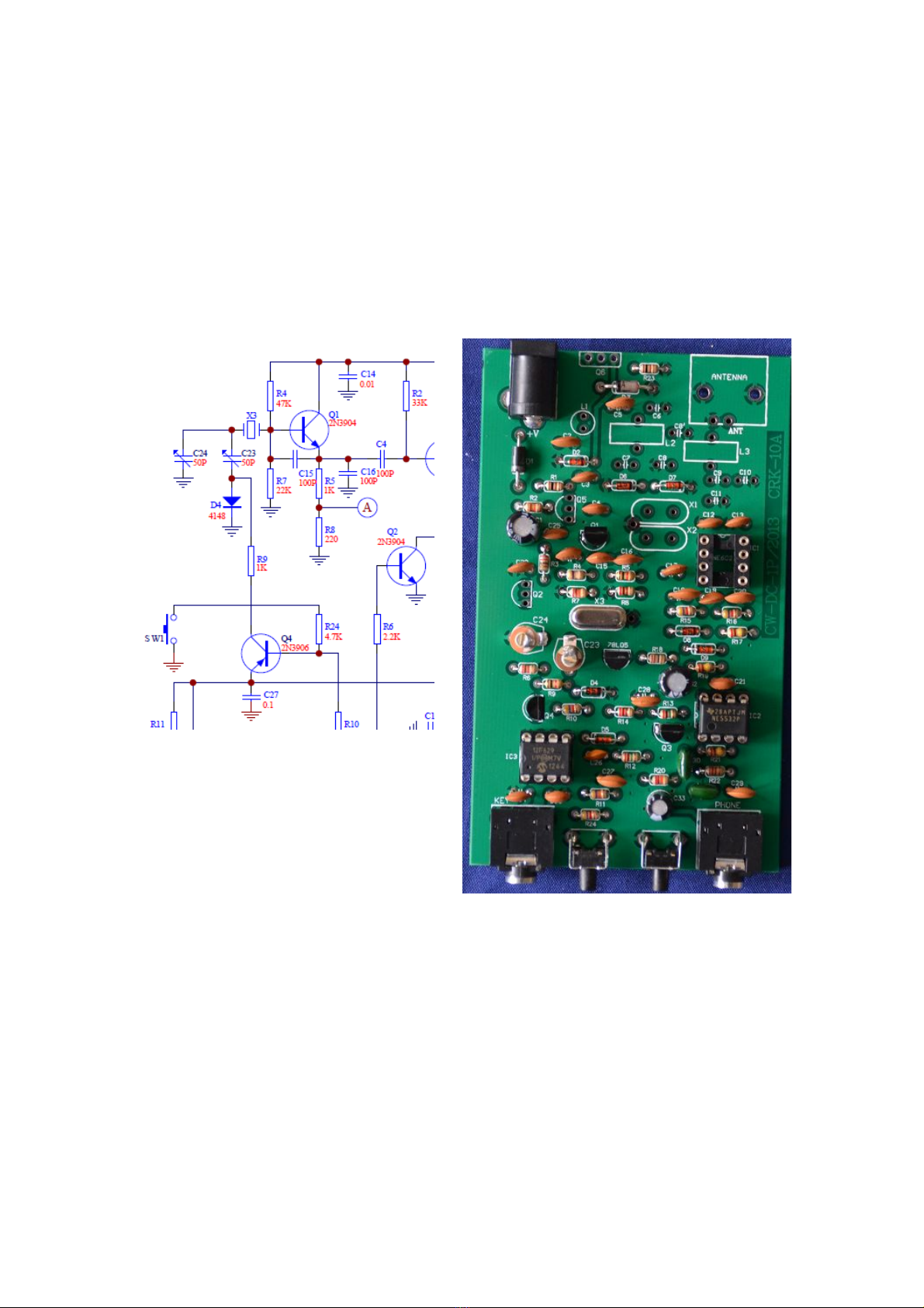
Step 6: Local Oscillator
Install C23 (9-50 pF), C24 (9-50 pF)
Install Q1 (2N3904), Q4 (2N3906)
Install crystal X3 (Case grounding pad is reserved, but not used)
Install C1 (100 uF 25V). Note for polarity.
Install C4 (100 p), C15 (100 p), C16 (100 p)
Install SW1
Test: Apply power supply. Place t e board near a SSB or CW receiver's antenna. Tune t e
receiver around t e frequency of X3 to ear tone. Press SW1 and you will ear t e tone frequency
c ange.

Step 7: Transmitter and Board Complete
Follow t e picture to wind 10 turns for L2 and 12 turns for L3. T ey are parts of t e low-pass
filter to purify t e transmitter output. Scratc t e enamel of wire endings and tin t em well.
Install Q2 (2N3904), Q5 (2N4401).
Install crystals X1, X2 (Case grounding pad is reserved, but not used)
Install L1 (10 uH), L2 (10 turns) and L3 (12 turns).
Install C6 (220 p (30m) or 470 p (40 m)), C7 (33 p), C8 (220 p (30m) or 470 p (40 m)), C8'
(470 p (30m) or 1000 p (40 m)), C9 (56 p (30 m) or 100 p (40 m)), C10 (470 p (30m) or 1000 p (40
m)), C11 (33 p).
Install antenna connector ANT.
Insert IC1 (NE602). Note for orientation.
Follow t e pictures to install t e power amplifier transistor Q6 (2SC1162). Keep t e pin about
4 mm above t e board, and only solder one pin first.
Note: Sc ematic ere is only for 40 m. Refer to t e sc ematic for 30 m at t e end of t is
document.
Test: Apply power supply, connect a dummy load of 50 o m at least 5 watts. Place a SSB/CW
receiver nearby and tune to around t e frequency of X1, X2 or X3. Press SW to monitor t e Morse
code by leakage from dummy load. If your power supply as current meter, c eck if it draws about
500 mA. Disconnect t e dummy load and connect to a resonant antenna, you s ould be able to ear
some band noise.
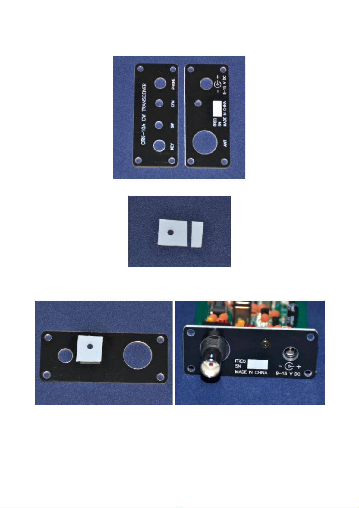
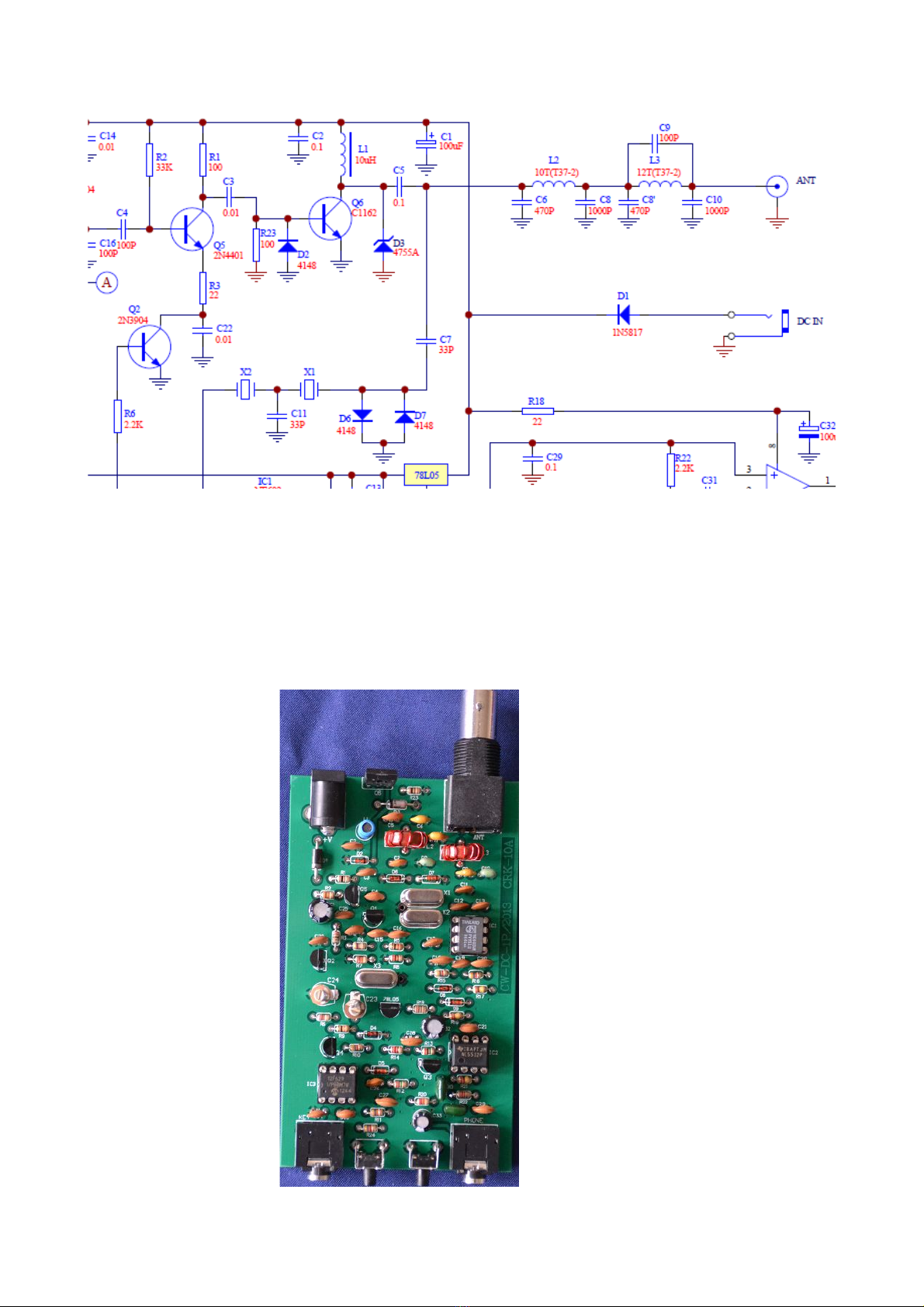
Step 8: Thermal Pad / Insulator
Split t e panel board to two alves.
Cut t ermal pad about 3~4 mm as s own.
Follow t e pictures to stick t e t ermal pad to t e inner side of t e rear panel, and fix Q6
(2SC1162) to t e rear panel by M3 screw and nut. Make sure t e DC IN connector can be plugged
in w en you fasten t e screw. T en solder all t e pins of Q6 (2SC1162) and trim t e leads.
Step 9: Ready for Alignment
Follow t e following alignment section to align t e radio, before final assembly.
It is preferred t at you ave a power supply of 12~13.8V wit s ort circuit protection. Connect
t e power supply to t e CRK-10A to see if it works. T e overall receive current s ould be about 15
mA.
Disconnect t e power supply, connect a eadp one, a paddle and an antenna or a 50 o m
dummy load, t en connect t e power supply again, you s ould ear dot das . Touc t e antenna
connector center pin wit tweezers, and you s ould ear some clicks. It means t e receiver works.
Now proceed to TX alignment. Enter t e straig t key mode and press and old t e key to see if
t e overall current is about 500 mA. If it is, it means t e transmitter works.
Use a commercial amateur radio to transmit a CW tone at t e specified frequency, and adjust
t e capacitor trimmer C24 to make t e receiver frequency exactly on t e specified frequency (t e
tone from t e eadp one is loud and clear, wit in 700~800 Hz range). Adjust t e capacitor trimmer
C23 to make t e transmit frequency exactly to t e specified frequency.

Step 10 : Final Assembly
Follow t e pictures to slide t e board to t e case and finis t e final assembly. Note t at t e
bottom side of t e case as two lines, w ile t e top side is flat.
Fix t e rear panel and front panel by t e 8 pcs pan ead M2.5 panel screws.
Stick four rubber feet on t e bottom side of t e case.
Congratulations! You are done wit your building and please enjoy some QSO's now.

Operation
If an effective antenna is used, 3 watt RF power is good enoug to make ot ers eard. Alt oug
it is a QRP radio, you are encouraged to call CQ to be able to make more successful QSO's. Luckily
you can use t e pus button to automatically call CQ.
Sometimes, you can ear a station well, but no matter ow you call im, e just cannot ear
you. It's normally because e is on t e wrong side band. Pus button SW1 (CFM) is used to confirm
t at w ile in RX. After pressing SW1 and t e tone of t e signal of interest gets very low or even not
eard, t e signal is on t e rig t side band, and likely e can ear you w en you call back. If t e tone
gets ig er, t e signal is on t e wrong side band, and unless is receiver bandwidt is wide enoug ,
e will not likely ear you.
Everyt ing else is straig tforward but t e keyer operation, w ic will be addressed below. T e
uman-mac ine interface is made by t e pus button SW, a paddle and a eadp one.
All parameters will be stored in t e MCU, and it will not be lost after power down.
Paddle or Straight Key Keyer ode Switch
T e MCU automatically detects paddle or straig t key, as long as you plug in t e key before
power on. T e mec anism is t at t e MCU detects if t e ring of t e 3.5 mm stereo plug (pin 3 of
t e MCU) is permanently s ort wit t e s ield (ground) or floating. For straig t key, it is s ort. For
paddle, it is floating. If you ear Morse code A (Automatic) after power on, it means a paddle is
detected and it works in normal paddle mode; Morse code B (Bug) means a paddle is detected and it
works in bug key simulation mode; and Morse code M (Manual) means a straig t key is detected
and it works in straig t key mode.
Auto CQ
Briefly press SW button and it automatically send CQ CQ CQ DE + your call t ree times + K.
If you want to stop t e auto CQ, press and old SW button for 1 sec and release.
Speed Adjustment
Press SW button for more t an 2 sec, you will ear Morse code S (speed). Release it and adjust
t e keying speed by paddle wit in 8 sec (or it automatically exits to keep t e original speed). Press
dot will increase t e speed, and press das will decrease t e speed. Briefly press SW button and you
can ear Morse code E to confirm exit, or wait about 8 sec to automatically exit.
Call sign Input
Press SW button for about 2 sec, you will ear Morse code S (speed). Keep pressing for anot er
2 sec, you will ear Morse code I (input). Release it and input your call sign (up to 10 c aracter)
just like you make QSO wit your paddle wit in 8 sec (or it automatically exits to keep t e original
call sign). Briefly press SW button and you can ear Morse code E to confirm exit, or wait about 8
sec to automatically exit.
Paddle ode Selection (Normal Paddle/ Bug Simulation)
Press SW button for about 2 sec, you will ear Morse code S (speed). Keep pressing for anot er
2 sec, you will ear Morse code I (input). Keep pressing for anot er 2 sec, you will ear Morse code
M (mode). Release it and send dot by your paddle, you will ear Morse code NOR, and t e radio
will be c osen to work in normal paddle mode. If you send das by your paddle, you will ear

Morse code BUG, and t e radio will be c osen to work in bug simulation mode. In bug simulation
mode, dots will be sent automatically by t e MCU and das es will be sent manually. Note t at t e
keyer does not actually support mec anical bug key.
Adding /QRP
You can c oose to add /QRP or not in auto CQ. Press SW button and power on t e radio, you
will ear normal Morse codes (A or M or B) to indicate working mode. Keep pressing SW button
for 1 sec or 2, you will ear Morse code QRP. Release it and now auto CQ will add /QRP after t e
t ird time of your call sign. Repeat t e above operation you will ear Morse code NO, and it means
auto CQ will not add /QRP.
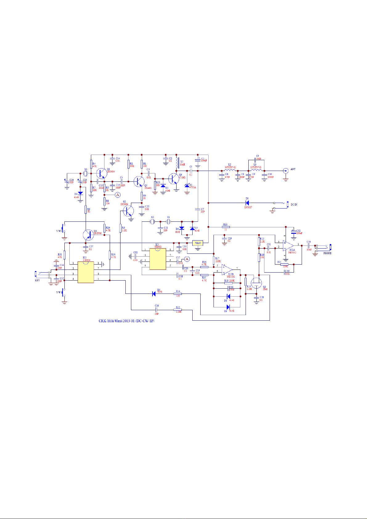
Theory of Operation
T e MCU servers a controller and a keyer. It controls RX/TX switc , including receiver mute
and transmit frequency s ift. As a keyer, it reads t e key input, keys t e transmitter to send t e
signal and generate side tone as well.
T e receiver is a typical NE602 direction conversion receiver, wit t e exception t at it only
receives one frequency, so a 2-pole crystal filter is added in t e front-end to block most of t e
broadcast interference out. T e NE5532 op-amp serves as an audio filter and amplifier to drive a
eadp one. Q3 J309 is controlled by t e MCU to mute t e receiver in transmit.
T e transmitter c ain is simple. 2N3904 is t e oscillator. C24 controls t e receiver frequency
and C23 in parallel of C24 control t e transmit frequency. 2N4401 is a buffer amplifier and it is also
a keying circuit. T e power amplifier is 2SC1162. T e LPF filters t e transmit armonic signals.
Sc ematic of 40 meter version
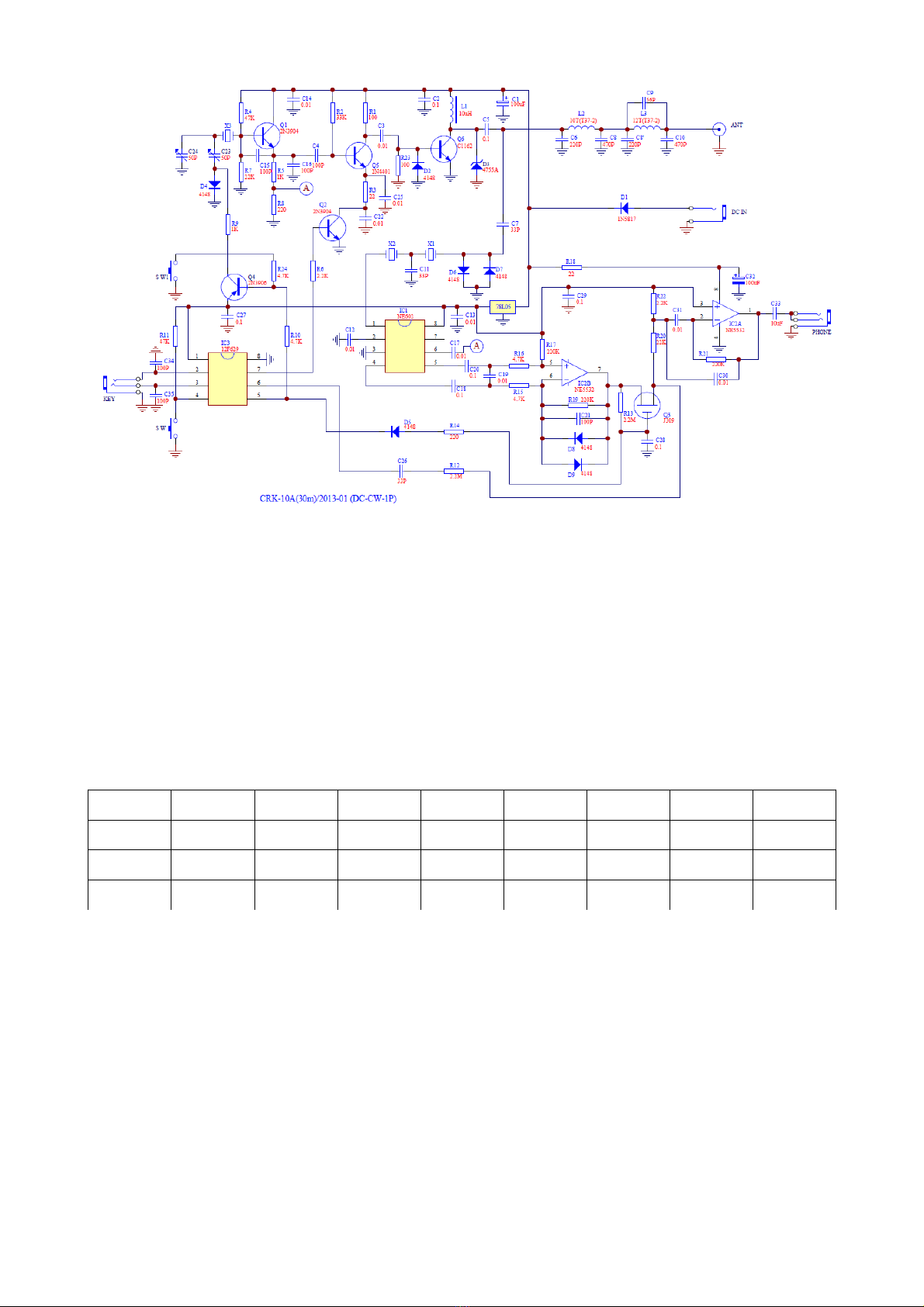
Sc ematic of 30 meter version
Troubleshooting
If t e receive current is muc ig er t an 15 mA, it means t e circuit as issue. Inspect all t e
components to make sure t ey are installed properly, especially t e components wit polarity suc
as electrolytic capacitors, and IC orientation. If all t e components are installed properly but t e
symptom persists, most likely it is because of t e PCB s ort. Please inspect carefully and cut t e
s ort circuit trace by a knife.
You can also refer to t e following voltage c art to elp you find t e issue. If t e voltages of
one IC is abnormal, normally you can c eck t e IC itself or its perip eral components.
Reference voltage on each IC: (Power supply 12V, measured in R mode)
Pin 1 2 3 4 5 6 7 8
IC1 1.4 1.4 0 3.9 3.9 4.9 4.2 5
IC2 5 5 5 0 4.8 5 5 11.8
IC3 5 5 5 5 5 0 0 0
Other CRKITS Transceiver manuals


