improvedthermalperformance
by
eliminating
the
insulating
interface
underneath
the
powerdevices.
The
chassis
itself
is
used
as
part
ofthe
thermalcircuit,
and
this
maximizesutilization
ofthe
availableresources.
Air
flow
in
this
amplifier
is
front
to
rear,
also
a
departure
from
other
Macro-Techs.
Fan
speed
isa
function
of
ODEPIevel.
AlthoughODEP
was
covered
in
detail
inthe
BASICSsection
of
thistext,
the
specif
icsof
the
MA-5000VZODEPcircuit
are
unique
and
will
be
coveredhere.
Notes
OUTPUT
STAGE
CIRCUITRY
The
MA-5000VZ,
like
otherMacro-Techs,uses
the
groundedbridge.
It
does
differ,
however,
in
certain
aspects.
For
example,quadrants
use
four
devices
¡n
parallel
ratherthan
the
normalmáximum
of
three.Output
stages
are
alsophysically
built
ina
modularway,
for
ease
of
field
replacement.
Electrically,there
are
also
a few
differences.
Biasservonetworks
consist
oftwo
transistordevices
perVbe
multiplier(one
setfor
highside,
one
setforlow
side).Also,ODEPaffects
thelow
side
as
well
asthe
high
side
by
stealing
low
side
bias
and
drive.Takingthat
a
stepfurther,
any
protective
action
which
limits,
mutes,
or
shutsdown
the
amplifierwill
accomplish
the
samething
by
stealingdrive.
Circuitry
onthe
positive
and
negativeoutputmodules¡ncludebias
circuitry,
current
limit
circuitry
(theMA-5000VZ
hastwo
speedcurrent
limit),
last
voltageamplifiers(LVA's),pre-driyers,drivers,
and
output
devices.Temperature
sensors
are
alsomounted
tothe
heatsinks
vía
the
outputmodules.Thesedeliver¡nformation
tothe
main
module
which
computesactualcalibratedtemperature
for
ODEP
and
temperature
measurement.
H-15V
R571
2.7K
Positive
(NPN)Output
Stage
Thermal
SensorCircuitry
U50O
V.
LM334
r
L
3
R572
r£
227
O.5OW
R584
2.7K
\
+TEMP1
:
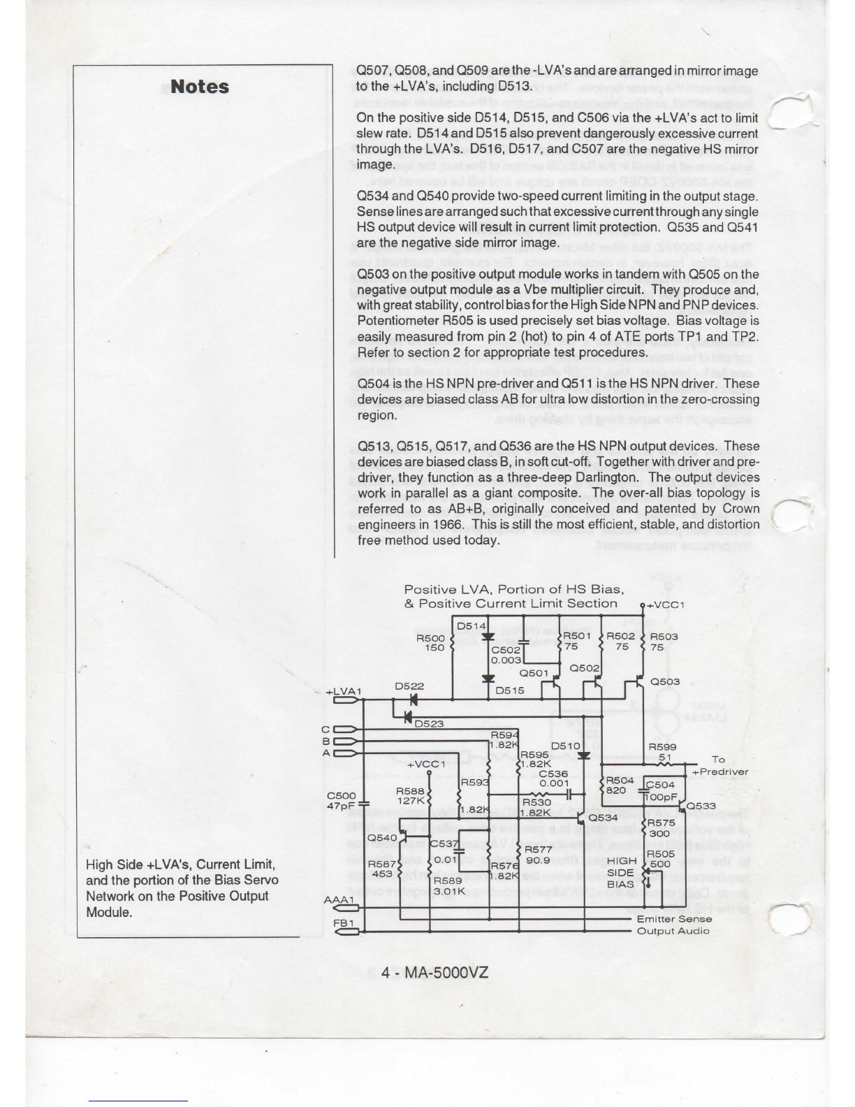
The
positive
LVA's
(Q501,
Q502,
and
Q503)convert
the
negative
output
of
the
voltagetranslatorstage
toa
positivedrivevoltage
fortheNPN
High
Side
(HS)predriver.There
are
three
LVAtransistorsin
parallel
due
to
the
very
high
voltages
(therefor
higher
current
and
thermal
requirements)that
are
present
when
the
power
supply
isin
highvoltage
mode.
D522
prevenís
the
+LVA'sfromproducinga
highnegativeoutput
totheHSNPN
stage.
MA-5000VZ
- 3