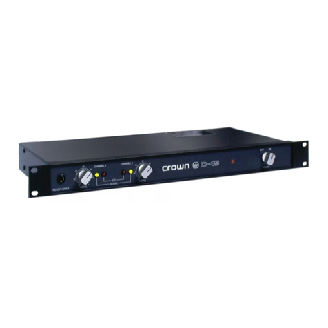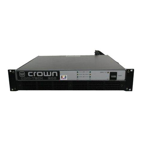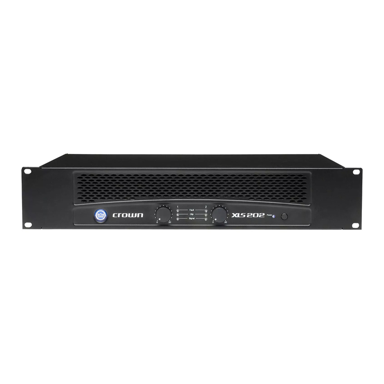
Power Base-1 & 460CSL Amplifier Service Manual
8
Theory
OVERVIEW
It should be noted from the outset that the PB-1 and
460CSL amplifiers are electrically and mechanically
identical products. The only differences, from a ser-
vice perspective, are cosmetic. For the purposes of
servicing the products, it should also be known that
the CSL version has been on the market since 1992.
SincethePBamplifiershavebeeninproductionsince
the mid-1980’s there are a number of electrical and
mechanicalpartsassociatedwiththeolderPBmodels
only.ItisalsoimportanttorealizethatovertimeCrown
has introduced numerous improvements to PB/CSL
amplifiers. Though often changes are minor, and are
madeforavarietyofreasons,afewchangeshavehad
a significant impact on the operation of the circuitry.
This manual is up to date as of the time of writing. For
additional information regarding these amplifiers, re-
fer to the applicable Technical Notes provided by
Crown for this product.
Thissectionofthemanualexplainsthegeneralopera-
tion of a typical Crown power amplifier. Topics cov-
eredincludeFrontEnd,GroundedBridge,andODEP.
Due to variations in design from vintage to vintage
(andsimilaritieswithotherproductsCrown)thetheory
of operation remains simplified.
FEATURES
Power Base/CSL amplifiers utilize numerous Crown
innovations including grounded bridge and ODEP
technologies. Cooling techniques make use of the
whatisessentiallyairconditionertechnology.Airflows
bottom to top, and front to side. Air flows a short
distance across a wide heatsink. This type of air flow
provides significantly better cooling than the “wind
tunnel” technology used by many other manufactur-
ers.Outputtransistorsareofthemetalcantyperather
thanplastic case. Thisallowsfor asignificantlyhigher
thermal margin for the given voltage and current
ratings. All devices used are tested and graded to
ensure maximum reliability. Another electronic tech-
nique used is negative feedback. Almost all power
amplifiers utilize negative feedback to control gain
and provide stability, but Crown uses multiple nested
feedback loops for maximum stability and greatly
improveddamping.MostCrownamplifiershavedamp-
inginexcessof1000inthebassfrequencyrange.This
feedback, along with our compensation and ultra-low
distortion output topology, make Crown amplifiers
superior.
Features specific to the Power Base/CSL Series’ in-
clude a single core transformer (one primary with two
independentungroundedsecondaries),afulltimefull
speed fan which also serves as the low voltage
transformer, slew rate limiting, and audio muting for
delay or protective action. This amplifier can operate
in either a Bridged or Parallel Mono mode as well as
dual (stereo). A sensitivity switch allows selection of
input voltage required for rated output. Level controls
arerearmounted.Theonlyindicatorprovidedtellsthe
operator that the low voltage supply is energized. In
general, the packaging of this model is designed for
maximum watt/price/weight/size value. It is the most
basic grounded bridge amplifier now available from
Crown.
Foradditionaldetailsrefertothespecificationsection,
or to the applicable Owner’s Manual.
FRONT END OPERATION
Thefront end iscomprised of threestages: Balanced
Gain Stage (BGS), Variable Gain Stage (VGS), and
theError Amp. Figure1 shows asimplified diagram of
a typical front end with voltage amplification stages.
Balanced Gain Stage (BGS)
Input to the amplifier is balanced. The shield may be
isolated from chassis ground by an RC network to
interrupt ground loops (early models did not have the
Ground Lift feature) via the Ground Lift Switch. The
non-inverting (hot) side of the balanced input is fed to
the non-inverting input of the first op-amp stage. The
inverting (negative) side of the balanced input is fed
to the inverting input of the first op-amp stage. A
potentiometerisprovidedforcommonmoderejection
adjustment. Electrically, the BGS is at unity gain.
(From an audio perspective, however, this stage
actually provides +6dB gain if a fully balanced signal
is placed on its input.) The BGS is a non-inverting
stage. It’s output is delivered to the Variable Gain
Stage.
Variable Gain Stage (VGS)
Note: Older models only had two front end stages.
The functions of this stage were combined, primarily,
with those of the third.
FromtheoutputoftheBGS,thesignalgoestotheVGS
where gain is determined by the position of the Sen-
sitivity Switch, and level is determined by the level
control. VGS is an inverting stage with the input being
fedto itsop-amp stage. Because gain after this stage
is fixed at 26dB (factor of 20), greater amplifier sensi-
