Cumbria Designs Minifilter User manual

CONTENTS
1 INTRODUCTION 2
2 PREPARATION 2
3 CIRCUIT DESCRIPTION 3
4 ASSEMBLY 4
5 TESTING 6
6 SET UP AND OPERATION 7
APPENDICES Schemat c A
Overlay B
Parts L st C
Troubleshoot ng D
Spec f cat ons E
Template F
M n f lter
DSP Aud o Processor
User Manual

M n f lter v1.0 Doc vers on 1.4 Page 2 of 14
© Cumbr a Des gns
1 Introduction
Thank you for purchas ng the Cumbr a Des gns “M n f lter” k t. Th s manual descr bes
the assembly and operat on of the M n f lter k t, even f you are a seasoned
constructor, please read th s manual and fam l ar se yourself w th the nstruct ons and
k t contents before commenc ng solder ng. If assembled carefully, th s un t w ll
prov de many years of rel able serv ce. We hope that you enjoy construct ng and
us ng your new M n f lter.
________________________________________________________________
2 Preparation
2.1 Tools
We recommend that the follow ng tools
are used dur ng assembly and test ng;
25W f ne t pped solder ng
60/40 Ros n cored solder
5” or smaller d agonal s de cutters
Small po nted nosed pl ers
Solder sucker (just n case!)
Mult meter
2.2 Conventions
The follow ng symbols are used w th n
the assembly nstruct ons to draw
attent on to cr t cal steps such as
component or entat on and ant -stat c
precaut ons. The assoc ated narrat ve
descr bes the act on requ red.
Cr t cal Step
Stat c Sens t ve
2.3 Assembly
The product on of a successful
f n shed work ng k t s dependent upon
careful component handl ng, careful
placement and good solder ng!
Don’t be tempted to rush the
construct on, even though th s s a
relat vely s mple k t, a wrongly placed
component can prov de hours of
frustrat ng fault f nd ng. Also, as th s k t
uses a double s ded Pr nted C rcu t
Board (PCB) w th through plat ng,
removal of a wrongly soldered part
can be d ff cult. Follow the assembly
nstruct ons carefully to avo d
m stakes.
2.4 Component Identification
All parts carry a coded dent ty to
descr be the r values. It s mportant to
be able to recogn se these dur ng
assembly. Capac tors have the r value
pr nted numer cally, e.g. 104 = 100nF,
103 = 10nF etc. Res stors have the r
values represented by coloured bands
– th s s a frequent source of
confus on!
To s mpl fy component dent f cat on,
the assembly notes carry the dent t es
of each component as t appears on
the dev ce. For res stors the colour
cod ng s g ven. Th s should be
referred to dur ng assembly to ensure
the r ght parts are placed n the r
respect ve pos t ons on the PCB.
2.5 Component Leads
Many of the pass ve components w ll
requ re the r leads to be formed to
al gn w th the holes on the PCB. Th s
ma nly appl es to the ax al parts such
as res stors and d odes. Form ng
component leads s eas ly done w th a
pa r of po nted nose pl ers and us ng
the hole spac ng on the PCB as a
measure. Alternat vely, small formers
made from scrap off cuts of Vero
board etc., make deal templates that
produce cons stent results. Some
parts, such as var able res stors, have
preformed leads des gned for mach ne
assembly. These w ll requ re
stra ghten ng to al gn w th the board
layout. Aga n, a pa r of po nted nose
!

M n f lter v1.0 Doc vers on 1.4 Page 3 of 14
© Cumbr a Des gns
pl ers should be used to carefully
flatten the factory perform ng to
produce stra ght leads.
2.6 Soldering
Before apply ng solder check carefully
that the co ponent you have
placed is in the right position! Th s
s a through plated double s ded
board. Wh lst some of the pads are
very small, the area presented by the
through plat ng s more than adequate
to allow good solder flow to form
mechan cally strong good electr cal
jo nts. However, these can be d ff cult
to undo, so please double check
placement!
The major ty of problems are l kely to
be caused by solder ng faults. These
can somet mes be d ff cult to f nd. Here
are some bas c golden rules that w ll
help you to avo d poor solder jo nts;
• Clean Iron
Make sure your solder ng ron t p s n
good cond t on and t nned. A small
mo stened pad for clean ng t ps,
regularly used to w pe off excess
solder and flux, w ll ensure that your
ron performs well. Remember to t n
the ron mmed ately after each w pe.
• Clean Leads and Pads
All of the component leads and PCB
pads n th s k t are pre-t nned and
should not need clean ng before
solder ng. Please ensure that parts are
handled so as to avo d contam nat on
w th grease or f ngerpr nts.
• Soldering
Th s s the b t that can tr p up even
exper enced constructors. For the
solder to fuse w th the surfaces to be
jo ned t s necessary for them to be
hot – but not so hot as to damage the
parts! It’s as s mple as 1-2-3;
1. Place the tip of the iron against
the joint, hold it there briefly to
bring the metal surfaces up to
temperature.
2. Apply the solder allowing it to
flow smoothly onto the
surfaces.
3. Remove the iron and inspect
the new joint.
The f n shed jo nt should have a
smooth sh ny coat ng of solder. If the
jo nt s dull grey or has formed a
spher cal “blob”, apply the ron to the
jo nt, remove the old solder w th a
solder sucker and re-solder.
3 Circuit Description
3.1 General
The M n f lter c rcu t compr ses of three
sect ons; an nput ampl f er (MCP618),
a m croprocessor (dsPIC33FJ) and an
output ampl f er (LM380). The nput
ampl f er n conjunct on w th the nput
level pot VR1 enables the M n f lter to
operate w th a w de range of nput
s gnal voltages. Th s offer flex b l ty n
us ng the M n f lter, allow ng t to be
used w th low level aud o sources such
as AF pre-amp outputs w th just a few
tens of m ll volts up to h gher level
sources such as headphone outputs
wh ch may produce a volt or more of
output. The m croprocessor performs
the analogue to d g tal s gnal
convers on, the f lter ng, aud o
process ng and convers on back to
analogue to dr ve the AF power
ampl f er. The var ous funct ons of the
M n f lter are selected by ground ng the
control nputs. Ground po nts are
prov ded on the control header for use
w th external sw tch controls. To
prevent damage to the m croprocessor
t s mportant that no voltages greater
than 3.3V are appl ed to the control
nputs.
3.2 Theory of peration
At the heart of the M n f lter s a 16b t
m croprocessor w th Analogue to
D g tal Converter (ADC) and an aud o
D g tal to Analogue Converter (DAC).
The m croprocessor samples the aud o
from the nput ampl f er 11,000 t mes a
second convert ng each aud o sample


M n f lter v1.0 Doc vers on 1.4 Page 4 of 14
© Cumbr a Des gns
nto numer cal values represent ng
ampl tude. These values or "samples"
are passed to a F n te Impulse
Response (FIR) f lter that appl es
l near phase 501 tap band pass
f lter ng. The f lter algor thm s based
upon a delay l ne along wh ch samples
traverse and at each "tap" are
mult pl ed a set of data constants
called a "kernel". The results of all of
the mult pl cat ons are summed to
produce the f lter output. The f ltered
aud o samples are then steered
through the deno ser and auto-notch
processes f selected. These two
programs are almost dent cal to each
other and are short adapt ve FIR f lters
that constantly adjust the r frequency
response to track any repet t ve
(coherent) components w th n the
aud o samples. The deno ser output s
the output of the track ng f lter, wh ch
because of ts narrow bandw dth
reduces random no se. The auto-notch
output s the aud o less the output of
the track ng f lter caus ng t to remove
any constant coherent s gnals.
Processed aud o samples are then
passed to the DAC for convers on
back to an analogue voltage to dr ve
the AF power ampl f er.
4 Asse bly
The follow ng assembly sequence s recommended. Th s allows most of the smaller
parts to be held n place w th the board turned over wh lst solder ng the unders de.
4.1 Fixed Resistors (Broad tolerance band shown in capitals)
2R7 R6, R10 Red, Mauve, Black, S lver (BROWN)
100R R2 Brown, Black, Black, Black, (BROWN)
470R R3 Yellow, Mauve, Black, Black (BROWN)
1K R8 Brown, Black, Black, Brown, (BROWN)
10K R1, R4, R5, R7 Brown, Black, Black, Red, (BROWN)
47K R9 Yellow, Mauve, Black, Red, (BROWN)
4.2 Diode
F t the 1N4004 supply protect on d ode D1 not ng or entat on marked on s lk screen.
4.3 Inductor
F t the 15uH ax al nductor (resembles a large brown res stor) n pos t on L1 next to
D1. Form leads at 90 degrees close to nductor body so as to al gn w th PCB holes.
L1 15uH Brown, Green, Black, S lver
4.4 IC Sockets
Ensure correct or entat on! Match ndex cut out on socket to board pr nt ng. T p;
solder one p n only then check pos t on ng before cont nu ng. Heat the solder and
repos t on f necessary. Two 14 p n sockets are prov ded to make the 28 p n socket
requ red for IC3.
a) F t the 2x14 p n sockets n 28 p n socket pos t on for IC3.
b) F t 8 p n sockets for IC4 and IC5.
4.5 SIL Resistor RN1
The or entat on of the 10K SIL res stor s cr t cal. Install w th the text s de of the SIL
package fac ng IC3 sockets. The spot mark ng p n 1 w ll be adjacent to C8.
!
!
!

M n f lter v1.0 Doc vers on 1.4 Page 5 of 14
© Cumbr a Des gns
4.6 Dipped Ceramic Capacitors
Small yellow body, 0.1” p tch. Used for general s gnal coupl ng and supply
decoupl ng. Use a magn f er to conf rm values, these are s m lar n appearance to the
10nF ceram cs!
100nF C2, C4, C5, C6, C7, C8, C9, C19 104
4.7 Dipped Ceramic Capacitors
Small yellow body, 0.1" p tch. Used for decoupl ng +12V supply nput, aud o nput
and AF ampl f er nput. Use a magn f er to conf rm values, these are s m lar n
appearance to the 100nF ceram cs!
10nF
C1, C11, C14
103
4.8 Variable Cermet Resistor
The pre-formed leads w ll requ re to be stra ghtened to f t. Remove the corrugat ons
by gently compress ng each lead w th a pa r of small pl ers.
10K Aud o Input Cermet VR1 103
4.9 +3V3 Regulator
Polar ty consc ous component, ensure that or entat on s correct. Carefully form leads
so as to be able to nsert the TO92 style regulator nto IC2 pos t on tak ng care to
al gn the body and leads w th the outl ne marked on the s lk screen.
3v3 regulator IC2 MCP1700
4.10 Polystyrene Capacitors
Rectangular body, no polar ty.
0.47uF C12, C16, C17 u47
4.11 Electrolytic Capacitors
Polar sed capac tors, observe the polar ty shown by the s lk screen. The negat ve
lead s marked by a str pe on the capac tor body.
10uF
C3, C10
100uF C13, C15
4.12 Tantalum Capacitor
Polar sed capac tor, observe the polar ty shown by the s lk screen. The pos t ve lead
s marked bold a bold l ne and a small "+" symbol.
10uF C18
4.13 Connectors
Recommended P n Header Connector or entat on s w th rear lock ng tab fac ng nto
the centre of the board. The AF Ga n header s mount w th rear tab adjacent to IC5.
a) F t the two, two p n headers +12V, AF, LS
b) F t the three way AF Ga n header AF_GAIN
c) F t the twelve way Controls header
!
!
!

M n f lter v1.0 Doc vers on 1.4 Page 6 of 14
© Cumbr a Des gns
4.14 +5V Regulator
Polar ty consc ous component, ensure that or entat on s correct. The regulator s
mounted vert cally w th the metal face towards the outs de edge of the PCB. Heats nk
not requ red.
+5V regulator IC1 MC7805CT
4.15 Integrated Circuits
Stat c sens t ve parts. D scharge yourself to ground before handl ng. Avo d wear ng
stat c generat ng cloth ng (e.g. wool, man made f bres etc) dur ng assembly.
Correct or entat on s essent al. IC p ns w ll need to be gently formed for correct
al gnment before nsert on nto sockets. IC p ns can be pushed nwards by plac ng the
dev ce on ts’ s de on a f rm surface, and gently press ng the body down aga nst the
p ns. When nsert ng parts, take care to check p n al gnment to prevent damage.
a) Insert IC3 dsPIC33F128GP802 Processor (28 p n DIL)
b) Insert IC4 MCP618 Operat onal Ampl f er
c) Insert IC5 LM380N-8 AF Power Ampl f er
4.16 Connector Assemblies
Connector shells and p ns are suppl ed to allow connect on of power and s gnal l nes
to the M crocode DSP. The use of good qual ty, colour coded, heat res stant, mult
stranded w re s recommended. To avo d acc dents, a colour code convent on should
be chosen to represent funct on, e.g. Red +ve supply, Black ground, str ped colours
controls etc.
The connector assembl es compr se of two components; the shell and the p ns. To
term nate a conductor f rst str p back about 2mm of nsulat on and t n the exposed
w re. Place the t nned end of the w re nto a p n such that the t nned w re s ts ns de
the nner pa r of tabs and the nsulat on s ts w th n the outer tabs. W th small po nted
nose pl ers carefully compress the outer tabs onto the nsulat on to hold the w re.
Repeat th s w th the nner tabs to gr p the exposed conductor. Very carefully solder
the exposed conductor n place tak ng care not to allow solder to flow onto the
lock ng tab.
F nally, nsert the p n nto the shell w th the small lock ng tab or entated to the face of
the shell w th the small cut outs. Push home unt l the lock ng tab snaps nto the cut
out. Should you need to remove a p n, gently press the lock ng tab n w th a small
screwdr ver or the end of a pa r of po nted nose pl ers. The p n w ll be released and
can be pulled out of the shell.
Asse bly co plete, well done! Now carefully check the co ponent
place ent and soldering work before oving on to testing.
5 TESTING
Before connect ng your M n f lter to your power supply for the f rst t me, carry out
these s mple checks to conf rm that the supply ra ls are clear of shorts to ground.
!
!

M n f lter v1.0 Doc vers on 1.4 Page 7 of 14
© Cumbr a Des gns
5.1 Electrical Tests
5.1.1 +12 Volt Input
W th a mult meter set to res stance, place the Red meter lead onto +12v and the
Black to Ground and check for a h gh res stance. Prov d ng there s not a short c rcu t
then all s well.
5.1.2 +5 Volt Rail
Carry out the res stance test on the output s de of the regulator (IC1) to check the
+5v ra l ensur ng that t s clear of shorts to ground.
5.1.3 +3.3 Volt Rail
Carry out the res stance test on the output s de of the regulator (IC2) to check the
+3.3v ra l ensur ng that t s clear of shorts to ground.
5.1.4 Powering Up
Connect a loudspeaker and AF ga n potent ometer (10K log) as shown n F g.1
6 SET UP AND OPERATION
6.1 Power and Audio Connections
6.1.1 Loud Speaker
The aud o output should be connected to a 4 to 8 Ohm mpedance loudspeaker.
6.1.2 AF Gain Potentio eter
The AF Ga n potent ometer s connected as shown above. Th s w ll produce
ncreas ng aud o output w th clockw se rotat on.
6.1.3 AF Input
A screened aud o cable should be used to connect the s gnal source to the AF Input
connector.
AF Source
S gnal
Screen
Speaker
Volume
Control
(front)
Ground
+12V
Controls
Fig. 1 Power and Aud o Connect ons

M n f lter v1.0 Doc vers on 1.4 Page 8 of 14
© Cumbr a Des gns
6.1.4 Power
Connect +12V to the power header observ ng the polar ty shown above. Advanc ng
the AF Ga n control should produce a not ceable h ss from the loudspeaker. If
noth ng s heard d sconnect and check the supply, loudspeaker and AF Ga n control
w r ng. Check the or entat on and placement of all ICs and electrolyt c capac tors.
6.2 Controls Header
GND
AN GND
DEN
GND
GRP
GND
FL5
FL4
FL3
FL2
FL1
GND Ground supply p n for external sw tch
DEN Deno ser, h gh = deno ser off , low = deno ser on
GND Ground supply p n for external sw tch
GRP F lter Group, h gh = w de, low = narrow
FL1..FL4 F lter select b ts
6.2.1 Filter Selection Controls
1=Open c rcu t or +3.3V log c h gh
0=Ground or log c low
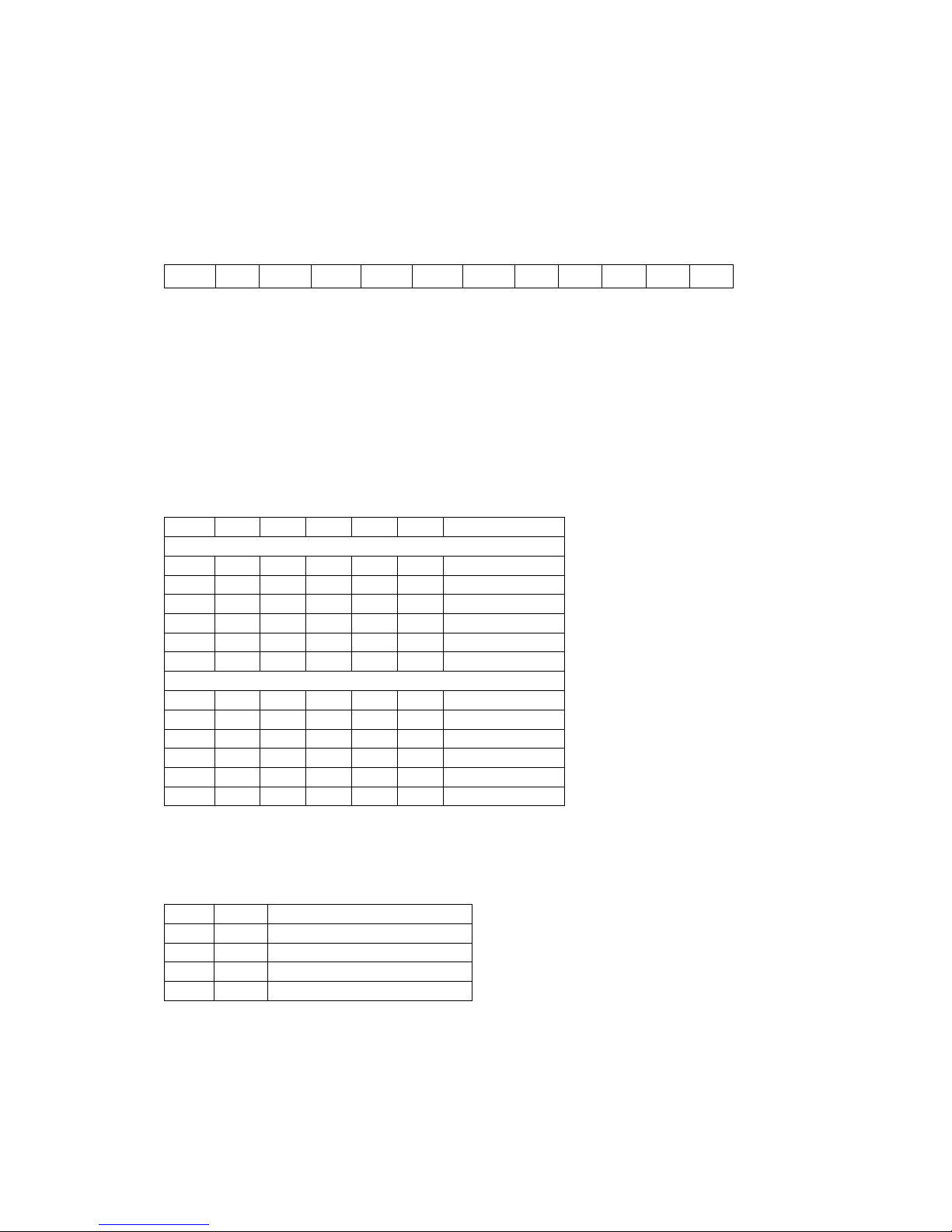
GRP
FL5
FL4
FL3
FL2 FL1
FILTER
W de F lter Group
1 1 1 1 1 1 300 - 2700Hz
1 1 1 1 1 0 300 - 2400Hz
1 1 1 1 0 1 300 - 2200Hz
1 1 1 0 1 1 400 - 2200Hz
1 1 0 1 1 1 400 - 2100Hz
1 0 1 1 1 1 450 - 2000Hz
Narrow F lter Group
0 1 1 1 1 1 400 - 900Hz
0 1 1 1 1 0 450 - 850Hz
0 1 1 1 0 1 500 - 800Hz
0 1 1 0 1 1 600 - 800Hz
0 1 0 1 1 1 500 - 700Hz
0 0 1 1 1 1 400 - 600Hz
6.2.2 Denoiser and Auto-notch Controls
1=Open c rcu t or +3.3V log c h gh
0=Ground or log c low
AN DEN Aud o Process ng
1 1 No aud o process ng
1 0 Deno ser
0 1 Auto-notch
0 0 Deno ser and Auto-notch
6.3 Control ptions
I portant! All M n f lter control nputs must be treated as "voltage free" nputs. In
other words they should only be operated by sw tches or dev ces such as open
collector trans stors so as not to apply an external voltage to the control port. W th no

M n f lter v1.0 Doc vers on 1.4 Page 9 of 14
© Cumbr a Des gns
control cond t ons appl ed all p ns are held h gh at 3.3V by the 10K SIL pull up
res stor. The ground p ns prov ded on the control port should be used as the sw tched
0V reference to pull any p n nto a log c low state.
The flex b l ty of the s mple control nterface allows many control scheme opt ons.
Several examples are g ven below.
6.3.1 Switched Control Sche es
Fig.2 Bas c Controls
A s ngle pole 6 way rotary sw tch and three toggle sw tches are used to access all of
the control states.
Fig.3 Us ng a rotary sw tch for Aud o Process ng controls
A 2 pole 4 way rotary sw tch replaces two toggle sw tches for Deno ser and Auto-
notch control.

M n f lter v1.0 Doc vers on 1.4 Page 10 of 14
© Cumbr a Des gns
Fig.4 Set of f lters from both groups selected by rotary sw tch
A two pole rotary sw tch prov des select on of f lters from both w de and narrow f lter
groups.
6.3.2 Microprocessor Control
The f lter and aud o process ng b ts may be controlled by an 8 b t w de port of an
external m croprocessor. Care must be taken to ensure that the log c h gh voltage of
+3.3V used by the M n f lter s not exceeded. If the external m croprocessor uses
3.3V log c then d rect connect on s poss ble. Ensure that the m croprocessor and
the M n f lter share a common ground.
If the external m croprocessor log c voltage s +5V then prov s on must be made to
protect the +3.3V control port of the M n f lter. Th s s conven ently done w th general
purpose d odes (1N4148, BAV21 etc) placed between the external m croprocessor
port and the M n f lter control port. The d odes are or ented w th the r cathodes (band)
towards the h gher voltage external m croprocessor port to block any current from
flow ng nto the M n f lter port dur ng a log c h gh state. The SIL pull up res stor on the
M n f lter control port w ll hold the control nputs at +3.3V.
6.4 Input Level
The nput level s set by adjust ng VR1, start w th VR1 set fully ant clockw se. If
connect ng to a po nt where the level s var able, e.g. a headphone socket on a
rece ver whose output s set by the rece ver AF ga n control, adjust the rece ver
output to normal l sten ng level. Next, connect the M n f lter and adjust VR1 slowly
clockw se (ensur ng the M n f lter AF Ga n s turned up so as to produce an output)
unt l aud o s heard. Cont nue unt l the aud o d storts sl ghtly (cl pp ng). Back off VR1
below the cl pp ng level.
If the M n f lter s to be used as a replacement aud o sect on n a rece ver t should be
connected to the output of the AF pre-amp stage before the rece ver's AF ga n
control. The rece ver's AF ga n control may be used as the M n f lter AF ga n control
by w r ng t as shown n F g.1.

M n f lter v1.0 Doc vers on 1.4 Page 11 of 14
© Cumbr a Des gns
6.5 perating Notes
The follow ng po nts w ll help you to get the best performance from your M n f lter;
• Set the M n f lter nput level just below that wh ch causes cl pp ng - ev dent as
a "crackl ng" on aud o peaks. Ma nta n ng a h gh nput level mproves the
performance of the deno ser and auto-notch.
• The deno ser operates on random no se only, any no se source w th a cycl cal
content w ll not be suppressed.
• Use the steep edges of the aud o f lters to remove adjacent s gnals that are
encroach ng nto the passband. For example, f an adjacent s gnal s caus ng
h gh frequency aud o nterference w th n the passband sw tch to the next
narrower f lter to lower the cut off frequency.

M n f lter v1.0 Doc vers on 1.4 Page 12 of 14
© Cumbr a Des gns
Appendix A Sche atic
Appendix B Co ponent Overlay

M n f lter v1.0 Doc vers on 1.4 Page 13 of 14
© Cumbr a Des gns
Appendix C Minifilter Version 1.0 Parts List
Res stors
2 2R7 R6, R10
1 100R R2
1 470R R3
1 1K R8
4 10K R1, R4, R5, R7
1 47K R9
1 10K CERMET TRIMMER VR1
1 10kx8 SIL RESISTOR RN1
Capac tors
3 10nF CERAMIC C1, C11, C14
8 100nF CERAMIC C2, C4, C5, C6, C7, C8, C9, C19
3 0.47uF POLYSTYRENE C12, C16, C17
1 10uF TANTALUM C18
2 10uF ELECTROLYTIC C3, C10
2 100uF ELECTROLYTIC C13, C15
Inductor
1 15uH CHOKE L1
Sem conductors
1 7805 +5V REGULATOR IC1
1 MCP1700 +3V3 REGULATOR IC2
1 DSPIC33FJ128GP802 PROCESSOR IC3
1 MCP618P OP AMP IC4
1 LM380N-8 AF POWER AMP IC5
1 1N4004 DIODE D1
Connectors
3 2 WAY HEADER +12V, AF, LS
1 3 WAY HEADER AF_GAIN
1 12 WAY HEADER CONTROLS
3 2 WAY SHELLS
1 3 WAY SHELL
1 12 WAY SHELL
21 CRIMP PINS
IC Sockets
2 8 PIN DIL IC4, IC5
2 14 PIN DIL IC3
M sc
PCB M n f lter v1.0
APPENDIX D Specifications
D mens ons W66mm, H47mm, D22mm (Overall w th connectors f tted)
Supply Voltage Nom nal +10V to +20V
Supply Current 54mA
Operat ng Temperature -20ºC to +70ºC

M n f lter v1.0 Doc vers on 1.4 Page 14 of 14
© Cumbr a Des gns
Appendix E Troubleshooting
Sy pto Action
No audio output • Confir supply on pin 7 and ground on
pin 4 of IC5
• Check IC5 place ent, soldering and
orientation, check soldering and
orientation of electrolytics
• Check soldering of AF Gain header and
wiring to AF gain pot
• Confir continuity and soldering of C16
and R9 and pin 23 of IC3
Controls not functioning
correctly
• Check soldering on controls header and
associated IC3 pins
• Re ove controls and confir input pins
at 3.3V
• Check orientation of RN1
• Check ground condition is being
applied as per tables in Section 6.2
Audio distorted • Reduce input level by turning VR1
anticlockwise
• Check orientation of C18
Appendix F Mark through te plate for preparing enclosure. Use centres as
guides, check and edit positions before drilling and cutting.
END
Table of contents