manuals.online logo
Brands
  1. Home
  2. •
  3. Brands
  4. •
  5. Curtiss-Wright
  6. •
  7. Measuring Instrument
  8. •
  9. Curtiss-Wright KAD/ADC/129/S2 User manual

Curtiss-Wright KAD/ADC/129/S2 User manual

Other Curtiss-Wright Measuring Instrument manuals

Curtiss-Wright D51615-202 Series User manual

Curtiss-Wright

Curtiss-Wright D51615-202 Series User manual

Curtiss-Wright SSR/CHS/001/B User manual

Curtiss-Wright

Curtiss-Wright SSR/CHS/001/B User manual

Curtiss-Wright SSR/CHS/001 User manual

Curtiss-Wright

Curtiss-Wright SSR/CHS/001 User manual

Popular Measuring Instrument manuals by other brands

Powerfix Profi 278296 Operation and safety notes

Powerfix Profi

Powerfix Profi 278296 Operation and safety notes

Test Equipment Depot GVT-427B user manual

Test Equipment Depot

Test Equipment Depot GVT-427B user manual

Fieldpiece ACH Operator's manual

Fieldpiece

Fieldpiece ACH Operator's manual

FLYSURFER VIRON3 user manual

FLYSURFER

FLYSURFER VIRON3 user manual

GMW TG uni 1 operating manual

GMW

GMW TG uni 1 operating manual

Downeaster Wind & Weather Medallion Series instruction manual

Downeaster

Downeaster Wind & Weather Medallion Series instruction manual

Hanna Instruments HI96725C instruction manual

Hanna Instruments

Hanna Instruments HI96725C instruction manual

Nokeval KMR260 quick guide

Nokeval

Nokeval KMR260 quick guide

HOKUYO AUTOMATIC UBG-05LN instruction manual

HOKUYO AUTOMATIC

HOKUYO AUTOMATIC UBG-05LN instruction manual

Fluke 96000 Series Operator's manual

Fluke

Fluke 96000 Series Operator's manual

Test Products International SP565 user manual

Test Products International

Test Products International SP565 user manual

General Sleep Zmachine Insight+ DT-200 Service manual

General Sleep

General Sleep Zmachine Insight+ DT-200 Service manual

Sensa Core Lacto Spark user manual

Sensa Core

Sensa Core Lacto Spark user manual

VOLTCRAFT UTS-1980 operating instructions

VOLTCRAFT

VOLTCRAFT UTS-1980 operating instructions

EBCHQ 94915 Operation manual

EBCHQ

EBCHQ 94915 Operation manual

Balluff BIP LD2-T017-01-EP-S4 Series user guide

Balluff

Balluff BIP LD2-T017-01-EP-S4 Series user guide

Pulsar IMP Lite Series instruction manual

Pulsar

Pulsar IMP Lite Series instruction manual

ETCR 6800 user manual

ETCR

ETCR 6800 user manual

manuals.online logo
manuals.online logoBrands
  • About & Mission
  • Contact us
  • Privacy Policy
  • Terms and Conditions

Copyright 2025 Manuals.Online. All Rights Reserved.

1
1 Jun. 2021 | DST/V/081 KAD/ADC/129/S2
CURTISSWRIGHTDS.COM
INFO: CURTISSWRIGHT.COM
EMAIL: DS@CURTISSWRIGHT.COM
KAD/ADC/129/S2
Full-bridge ADC (voltage excitation, programmable analog gain,
sense lines, 25kHz b/w) - 4ch at 100ksps
Key Features
•Four full or ½-bridge, potentiometer or
differential ended input channels
•Programmable input range (±10mV to ±10V)
•High accuracy (0.02% FSR typical for range of
1V and 10V)
•Programmable voltage excitation with
separate sense lines and balance adjust
•Short on any channel does not affect others
•16-bit simultaneous sampling on each channel
Applications
•Bridge sensors and strain gage measurement
•Differential voltage measurement
Overview
The KAD/ADC/129/S2 has four channels of signal conditioning and data
acquisition for differential voltages, strain gage or bridge measurements.
In addition to the measurement channel, the KAD/ADC/129/S2 provides
independent bipolar excitation for up to four channels. Each differential
ended signal has a separate programmable amplifier, filter and A/D
converter.
At the heart of the KAD/ADC/129/S2 is a hard-wired state-machine that
over-samples all channels at a rate between 200ksps and 400ksps and
digitally filters any noise above the user-programmable cutoff frequency.
This is achieved using cascaded, half-band, decimate by 2 x 15-tap,
Finite-Impulse-Response (FIR) filters followed by an 8th order Butterworth
Infinite-Impulse-Response (IIR) filter with a default cutoff point set at a
quarter of the sampling frequency. All signals are sampled simultaneously.
Thus, when several channels are sampled at different sampling rates, all
channels will be aligned at the start of an acquisition cycle.
The KAD/ADC/129/S2 is intended for use with strain gages, and should
not be used for asymmetric bridge transducers such as accelerometers,
pressure transducers unless sensor re-calibration is carried out on a
channel-by-channel basis. If the sense lines or internal offset adjust
(balance feature) are not required, refer to the KAD/ADC/129/S1.
Figure 1: First of four channels on the KAD/ADC/129/S2
ANALOG(0)
EXC_V(0)+
KAD/ADC/129/S2
ANALOG

DIGITAL
COUNTS

UNITS
+
-
DIGITAL

ANALOG


GAIN [1, 10, 100, 1000]
INST. AM P AAAF DIGITAL FILT ER LOOKUP TABLE
34.8K [R ADJ ]
VADJ
DIGITAL

AN ALOG VREF
+
-
+
-
+
-
STANDARD BUS INTERFACE AND LOGIC
51
GND
1
2
5
4
3
6
SENSE(0)+
+
EXC_V(0)-
SENSE(0)-
+
-
-
KAD/ADC/129/S2
2
1 Jun. 2021 | DST/V/081
CURTISSWRIGHT.COM © 2021Curtiss-Wright. All rights reserved. Specifications are subject to change without notice.
All trademarks are the property of their respective owners.
Specifications
All values provided in the following specification tables are valid within the operating temperature range specified under
“Environmental ratings” in the “General specifications” table. Module specifications are met for up to 97% of Full Scale Range
(FSR).
TABLE 1 General specifications
PARAMETER MIN. TYP. MAX. UNITS CONDITION/DETAILS
Slots – – 1 – Can be placed in any user-slot in any combination.
Mass
– 90 – g
– 3.17 – oz Design metric is grams.
Height above chassis For recommended clearance requirements see the
CON/KAD/002/CP data sheet.
bare connector – – 11 mm
bare connector – – 0.43 in. Design metric is millimeters.
Access rate – – 2 Msps Maximum combined access rate for read and write.
Power consumption
+5V 100 – 180 mA
+7V 15 – 30 mA Excludes current used by excitation.
-7V 10 – 25 mA Excludes current used by excitation.
+12V 50 – 80 mA
-12V 40 – 70 mA
total power 1.75 – 3.09 W Particular combinations of chassis and Acra KAM-500
modules may have power or current limitations. For details,
see TEC/NOT/016 - Power dissipation, TEC/NOT/049 - Power estimation,
and the relevant chassis data sheet.
Environmental ratings See Environmental Qualification Handbook.
operating temperature -40 – 85 °C Chassis base/side plate temperature.
storage temperature -55 – 105 °C
TABLE 2 Differential ended analog inputs
PARAMETER MIN. TYP. MAX. UNITS CONDITION/DETAILS
Inputs – – 4 –
Sampling rate While the sampling rate can be set individually, each must
have a power of two times any other (¼, ½ ...2, 4).
ANALOG[3:0] 2 – 100,000 sps
Input voltage
operating range (Gp = 1) -10 – 10 V Primary gain = 1.
operating range (Gp = 10) -1 – 1 V Primary gain = 10.
operating range (Gp = 100) -100 – 100 mV Primary gain = 100.
operating range (Gp = 1000) -10 – 10 mV Primary gain = 1000.
overvoltage protection -40 – 40 V Voltages outside of this range can damage input.
KAD/ADC/129/S2
3
1 Jun. 2021 | DST/V/081
CURTISSWRIGHT.COM
DC error DC signal averaged over 200 samples without excitation.
gain = 1, 10 – 0.02 0.08 %FSR
gain = 2, 20 – – 0.14 %FSR
gain = 4, 40 – – 0.25 %FSR
gain = 8, 80 – – 0.44 %FSR
gain = 100 – 0.04 0.18 %FSR
gain = 200 – – 0.33 %FSR
gain = 400 – – 0.6 %FSR
gain = 800 – – 1.2 %FSR
gain = 1000 – 0.3 1.5 %FSR
AC gain error Note that the figures presented here include analog anti-
aliasing filter and digital filter amplitude errors. For gain
≥1000, an additional error exists, which is caused by a much
lower bandwidth of instrumentation amplifier for that gain,
which is typically 60kHz (-3dB point), and has the shape of a
1st order filter.
– 0.02 0.1 %FSR For fin ≤ 3kHz, fs= 100kHz, fc= fs / 4 (fin: input signal
frequency; fs: sampling frequency; fc: filter cutoff frequency).
– 0.1 0.35 %FSR For 3kHz < fin ≤ 10kHz, fs= 100kHz, fc = fs / 4.
– 0.35 0.8 %FSR For 10kHz< fin ≤ 15kHz, fs= 100kHz, fc = fs / 4.
Effective number of bits
gain = 1, 10 12 13.5 – bits fc ≤ 25kHz and secondary gain of 1 (fc: filter cutoff
frequency).
gain = 100 11.5 12.5 – bits fc ≤ 25kHz and secondary gain of 1.
gain = 1000 9 10.5 – bits fc ≤ 25kHz and secondary gain of 1.
Crosstalk
gain = 1, 10, 100 – -100 -90 dB fin ≤ 25kHz and secondary gain of 1.
gain = 1000 – -80 -72 dB fin ≤ 25kHz and secondary gain of 1.
Common mode
voltage range -10 – 10 V Operational voltage range.
rejection ratio 72 80 – dB Applies within the above common mode voltage range, 0 f
fc.
Analog filter Analog filter is Butterworth.
poles – – 6 –
filter cutoff -3dB 38 40 42 kHz
Digital filter Digital filter is Butterworth.
poles – – 8 –
filter cutoff -3dB 0.25 – 16 fsThe maximum value is limited to 25kHz (fs: sampling
frequency).
0.1dB bandwidth – 0.8 – fc
aliasing to 0.1dB band – – -80 dB
aliasing to fc– – -80 dB
TABLE 2 Differential ended analog inputs (continued)
PARAMETER MIN. TYP. MAX. UNITS CONDITION/DETAILS
KAD/ADC/129/S2
4
1 Jun. 2021 | DST/V/081
CURTISSWRIGHT.COM
Filter delay – 200 – µs Where fin = fc = 10kHz (fin: input signal frequency).
Input resistance
between inputs 10 – – MΩ Whether module powered on or off.
single ended input to GND – 34.8 – kΩ Module powered on Measured on ANALOG(x)- input.
single ended input to GND 43 52 – kΩ Module powered off. Measured on ANALOG(x)- input.
single ended input to GND 10 – – MΩ Whether module powered on or off. Measured on
ANALOG(x)+ input.
Input impedance
between inputs – 300 – kΩ Module powered on (measured at 3kHz).
single ended input to GND – 300 – kΩ Module powered on (measured at 3kHz).
TABLE 3 Bipolar DC voltage excitation outputs
PARAMETER MIN. TYP. MAX. UNITS CONDITION/DETAILS
Outputs – – 4 – Applied per channel.
Output voltage
operating range 0 – 5.1 V Bi-polar excitation: 5V is 10V across the bridge.
resolution – 1.8 – mV Bi-polar excitation: 1.8mV is 3.6mV across the bridge.
compliance – – 30 mA Per channel.
short circuit current – – 125 mA
short circuit duration ∞ – – s
DC error
error – 0.1 0.3 %FSR With a constant 350Ω load.
noise (gain = 1) – – 0.5 mVrms As measured on analog input.
noise (gain = 10) – – 0.05 mVrms As measured on analog input.
noise (gain = 100, 1000) – – 0.01 mVrms As measured on analog input.
Output resistance – 0.2 – Ω
TABLE 2 Differential ended analog inputs (continued)
PARAMETER MIN. TYP. MAX. UNITS CONDITION/DETAILS
KAD/ADC/129/S2
5
1 Jun. 2021 | DST/V/081
CURTISSWRIGHT.COM
TABLE 4 Balance current outputs1
PARAMETER MIN. TYP. MAX. UNITS CONDITION/DETAILS
Outputs – – 4 – Applied per channel. Connected internally with
corresponding ANALOG(x)- input.
Output current
operating range -71 – 71 µA
resolution – 35 – nA
DC error
error – – 2 %FSR With a constant 175Ω load. The impact of this error on the
channel reading is less than 0.01%FSR (200 times lower
than the error specified here).
drift – – 0.15 %FSR Over temperature.
noise (gain = 1) – – 0.5 mVrms As measured on analog input.
noise (gain = 10) – – 0.05 mVrms As measured on analog input.
noise (gain = 100, 1000) – – 0.01 mVrms As measured on analog input.
Output resistance – 34.8 – kΩ
1. The balance line is permanently connected to ANALOG(x)- input. The line is intended for balancing strain gages, so the module
should not be used for asymmetric bridge transducers such as accelerometers or pressure transducers unless sensor re-calibration
is carried out on a channel-by-channel basis.
KAD/ADC/129/S2
6
1 Jun. 2021 | DST/V/081
CURTISSWRIGHT.COM
Setting up the KAD/ADC/129/S2
All module setup can be defined in XML using XidML® schemas (see http://www.xidml.org).
Instrument settings
Parameter definitions
Configurable parameters
AnalogIn(3:0)
NOTE: It is recommended that names are less than 20 characters, have no white space or contain any of the following five char-
acters "/><\.
SETUP DATA CHOICE DEFAULT NOTES
Manufacturer - - -
Name ACRA CONTROL ACRA CONTROL Name of manufacturer.
PartReference KAD/ADC/129/S2 KAD/ADC/129/S2 The instrument part reference.
SerialNumber AB1234 AB1234 Unique name for each module.
Channels - - -
AnalogIn(3:0)
Analog Input - - -
Settings - - -
Filter Cutoff
0.25
0.5
1
2
4
8
16
0.25
Required cutoff point for the filter is the chosen value
multiplied by the user sampling frequency. 0.25 is
recommended as any higher may lead to aliasing. 1
is the sampling rate.
Excitation Amplitude 0 to 5.1 0.2
Required excitation (in V) for the top of the bridge.
Excitation is bipolar so entering 5V means 10V
across the bridge.
Balance.Type CurrentShunt CurrentShunt Specifies the balance type to be carried out on the
bridge.
Balance.Applied -71e-6 to 71e-6 0 Shunt current (in A) applied to the bridge.
Balance.BalanceThisTime True
False False Specifies if balancing should be carried out this time
by software.
Balance.Tolerance 0.01 to 99.99 0.1
Specifies acceptable tolerance of achieved value vs.
target value, expressed as percentage of defined
input range.
Balance.Target -10 to 10 0 Specifies a value. that the channel should be
balanced to.
ShuntCurrent.Applied -71e-6 to 71e-6 0 Shunt mode current (in A) added to the bridge
NAME/DESCRIPTION BASE UNIT DATA FORMAT BITS REGISTER DEFINITION
AnalogIn(3:0) Parameters
AnalogIn
Analog signal data Volt OffsetBinary 16 R[15:0]
SETUP DATA CHOICE DEFAULT NOTES
Range Maximum -10 to 10 10 Range maximum for analog channel
Range Minimum -10 to 10 -10 Range minimum for analog channel
KAD/ADC/129/S2
7
1 Jun. 2021 | DST/V/081
CURTISSWRIGHT.COM
Getting the most from the KAD/ADC/129/S2
Wiring configurations
Figures 2 to 4 show possible wiring configurations for the KAD/ADC/129/S2.
Figure 2: Second of 4 independent ½-bridge channels with matched pair completion resistors
Figure 3: Third of 4 independent potentiometer channels
Figure 4: Fourth of 4 independent differential ended channels
EXC_V(1)-
ANALOG(1)-
ANALOG(1)+
KAD/ADC/129/S2
+
-
ANALOG
DIGITAL
COUNTS
 UNITS
+
-
DIG IT AL
ANAL OG


SENSE(1)-
GAIN [1, 10, 100, 1000]
INST. AMP AAAF DIGITAL FILTER LOOKUP TABLE
34.8K [R
ADJ]
VADJ
DIGITAL
ANALOG VREF
+
-
EXC_V(1)+
+
-
+
-
STANDARD BUS INTERFACE AND LOGIC
SENSE(1)+
51
7
8
11
10
9
12
EXC_V(2)-
ANALOG(2)-
ANALOG(2)+
KAD/ADC /129/S2
+
-
ANALOG

DIGITAL
COUNTS

UNITS
+
-
DIGITAL

ANALOG


SENSE(2)-
GAIN [1, 10, 100, 1000]
INST. AM P AAAF DIGITAL FILTER LOOKUP TABLE
34.8K [RADJ ]
VADJ
DIGITAL

ANALOG VREF
+
-
EXC_V(2)+
+
-
+
-
STANDARD BUS INTERFACE AND LOGIC
SENSE(2)+
51
GND
13
14
17
16
15
18
ANALO G(3)-
ANALOG(3)+
KAD/ADC/129/S2
+
-
ANALOG

DIGITAL
COUNTS

UNITS
+
-
DIGITAL

ANALOG


GAIN [1, 10, 100, 1000]
INST. AM P AAAF DIGITAL FILTER LOOKUP TABLE
34.8K [RAD J ]
VADJ
DIGITAL

ANALOG VREF
+
-
+
-
+
-
STANDARD BUS INTERFACE AND LOGIC
51
GND
19
20
21
24
23
22
KAD/ADC/129/S2
8
1 Jun. 2021 | DST/V/081
CURTISSWRIGHT.COM
Bias current return path
As shown in Figure 4 on page 7, the analog inputs can be used as differential inputs (that is, not from a bridge). In this case, if
the signal source is isolated with respect to the Acra KAM-500 (for example a battery), a common-mode resistance between the
negative input and ground (GND) should be used to provide a return for bias currents and reduce common-mode noise pick-up.
Because the bias currents are in the order of nAs resistors up to 10kΩcan be used. In most cases a short (0Ω) is recommended.
NOTE: When analog inputs are used as differential inputs, setting the excitation and balance to zero reduces quiescent currents
of the module.
Using high primary gains
For gains above 1000, the gain-bandwidth product of the amplifier reduces the bandwidth of the instrumentation amplifier to
approximately 60kHz. The effect of attenuation can be seen for input signals with frequencies of 10kHz and higher.
Excitation setup
Excitation can contribute error to the overall measurement, so it is recommended to use as close as possible to full-scale
excitation, to minimize the percentage error.
For optimal accuracy ensure each channel uses its corresponding excitation. If the excitation is not used, it should be set to the
minimum value.
Excitation drift on potentiometer configurations
Curtiss-Wright recommends a full-bridge input configuration for the KAD/ADC/129/S2. With this configuration the differential
input amplifier removes common mode voltage or common mode pickup noise on the input lines.
For potentiometer circuits where the negative input is tied to ground, excitation drift can have a direct impact on the input signal
either as a gain or an offset error. Note that excitation can drift up to 0.3% on an FSR of 5.1V. In the case where both excitation
lines drift in the same direction an offset error is seen in the measurement. The worst case possible offset is 0.3% of 5.1V and
results in a worst case 15.3mV offset of the measurement. This does not happen with full-bridge configurations. We recommend
that the negative input is tied to ground as shown in Figure 3 on page 7. If the negative input is floating, the drift of the
digital/analog converter related to the balancing input directly adds further offset error to the measurement.
Source load error caused by the balance adjust circuit
The balance circuit has an impedance of RADJ and is connected to the ANALOG(x)- input of the module. This connection is
performed internally on the module. In some bridge configurations, RADJ loads the source signal causing a quantifiable error. An
example schematic for a full-bridge configuration loaded with balance resistance is shown in the following figure.
Figure 5: Full-bridge configuration loaded with balance resistance
EXC_V(x)+
DIGITAL

ANALOG
34.8 K
R1 R2
R3 R4
To Inst Amp In-
V-
Vadj
V+
Rp = R2 // R4
Radj
EXC_V(x)-
(*)
Connection betw een V- and Radj is internal or external depending on module
(*)
ANALOG(x) -
To Inst Amp In+
ANALOG(x)+
KAD/ADC/129/S2
9
1 Jun. 2021 | DST/V/081
CURTISSWRIGHT.COM
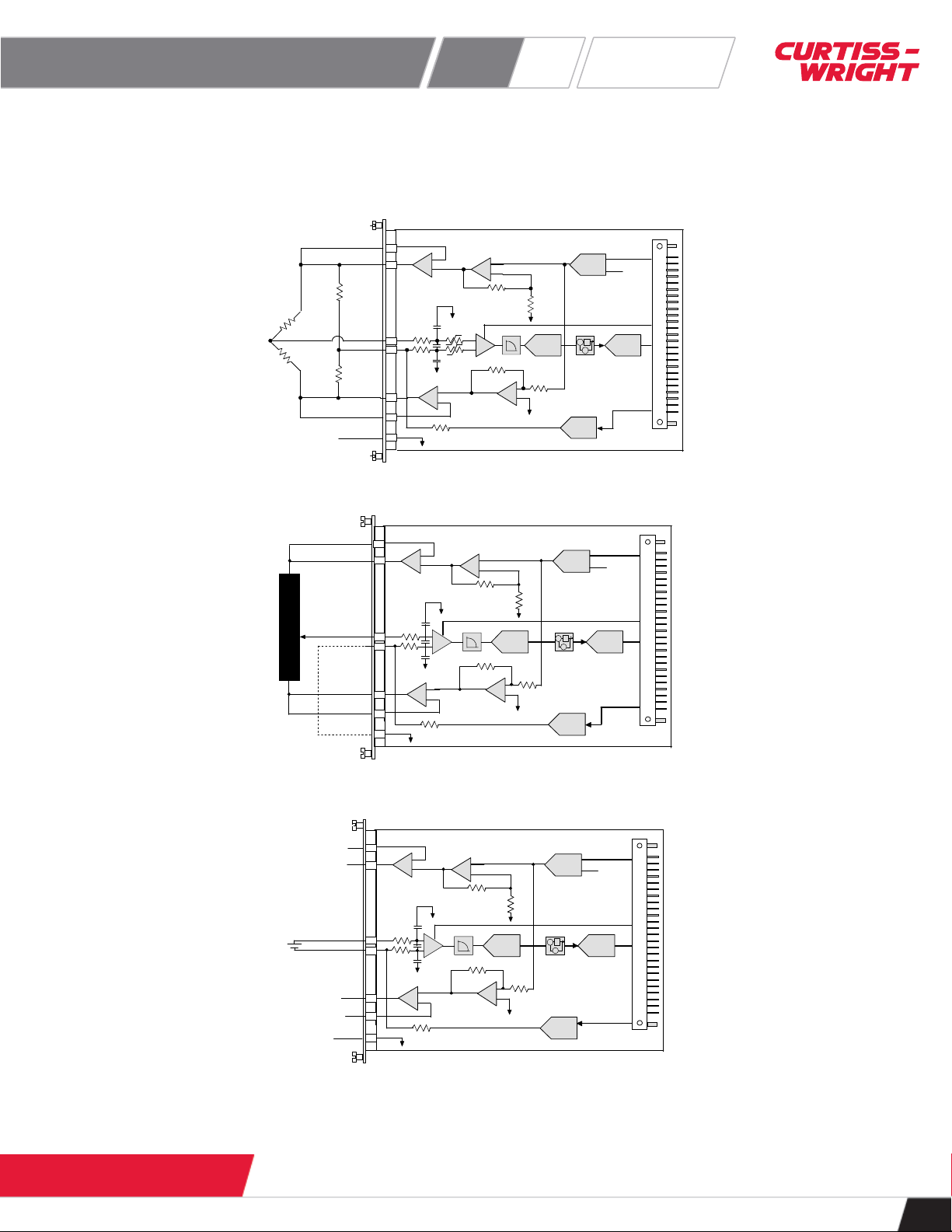
The DC error specification is checked as a differential input, so it does not include loading by RADJ which causes an additional
gain error.
In the previous figure, the gain error only occurs when the active leg of the bridge is connected to ANALOG(x)-. In this situation,
ANALOG(x)- is loaded by RADJ, forming a resistor divider with the resistance of bridge visible from the ANALOG(x)- input.
The gain error on ANALOG(x)- input can be quantified as follows:
where RP = R2 in parallel with R4
This additional gain error depends on the resistance of the bridge and can be typically -0.5% for a 350Ω bridge with its active leg
connected to ANALOG(x)-, and -0.172% for a 120Ω bridge.
In the case of a full-bridge with two active legs, only one leg of the bridge is affected. Therefore the gain error of voltage across
the bridge is half of the above quoted figures, that is, -0.25% for a 350Ω bridge.
For a symmetrical input range, the error can be expressed as %FSR error by further dividing the value by two, yielding to
±0.125% FSR for a 350Ω bridge.
Note that the gain error due to RADJ does not apply when:
•using a wheatstone bridge with the active elements (typically strain gages) placed only on the leg of the bridge connected to
ANALOG(x)+
•the leg of the bridge connected to ANALOG(x)- is populated with completion resistors (half-bridge with completion resistors)
•using only differential ended inputs with signal source isolated from module ground
•using only inputs in single ended configuration, connecting the signal to ANALOG(x)+ (ANALOG(x)- must be connected to
ground). This data sheet shows an example potentiometer application, which is not affected by this gain error.
Modules with RADJ connected externally might show this additional gain error offset but only if the balance adjust circuit is used
and in the cases stated previously.
NOTE: Gain error can be compensated at post processing, as the nominal resistance of the bridge is known.
Understanding filter delays
The Acra KAM-500 uniquely samples all signals at the start of an acquisition cycle and at equal intervals of time thereafter.
Signals sampled at the same sample rate will always be sampled at the same time independently of how they are stored or
transmitted. (This has significant advantages for issues such as time correlation.) However, before signals are sampled they are
filtered to remove noise components that might alias. The recommended cutoff point is one quarter the sampling frequency, as
this results in the maximum filtering of aliasing frequencies.
The Acra KAM-500 filters signals using over-sampling signal processing techniques. The figure below shows a delay for an 8th
order filter where fc = 1kHz. All filters cause a delay inversely proportional to the filter cutoff frequency (fc), so to calculate the
delay for other fc values, multiply the delay by (1kHz / fc). The frequency axis then needs to be rescaled to the new fc by dividing
the frequency values by (1kHz / fc). For example, an 8th order Butterworth filter with an fc of 1kHz delays a 1kHz signal by 1ms; a
filter with an fc of 10Hz delays a 10Hz signal by 0.1s. The delay for IIR filters (for example Butterworth) varies with the input
frequency.
%100








adjP
P
RR
R
Error
KAD/ADC/129/S2
10
1 Jun. 2021 | DST/V/081
CURTISSWRIGHT.COM
Figure 6: Filter delay for 8th order Butterworth filter where fc= 1kHz
The filter delay for the KAD/ADC/129/S2 is:
TD is the filter delay
TA (analog filter delay)  0
Additional delay sources
Primary gains higher than 10 cause an additional delay from 1st order filters in the instrumentation amplifier. That additional delay
is in the order of 0.25μs, for a gain of 100, and 2.5μs for a gain of 1,000.
In applications where time correlation is more important than suppression of aliasing, set the same cutoff point on all channels,
even if the sampling rates are different.
Sense lines
Sense lines are used to eliminate error due to voltage drop across lead resistance. Sense lines can not be left unconnected; they
should be connected as close as possible to the bridge. If however, the sense lines are connected close to the module (that is,
far from the bridge) and the lead resistance can be measured or estimated, add the voltage drop across the leads to the
excitation voltage. For example, for 0.5Ω leads in a 350Ω full-bridge where ±5V (10V) is desired across the bridge, the excitation
must be set to 5V + (0.5 × 10/350) = ±5.014.
kHz
milliseconds

fT
f
TT hButterwort
C
AD 8
1