CYPRES WICED CYW920706WCDEVAL Installation manual

Looking for a discount?
Check out our current promotions!
This coversheet was created by Verical, a division of Arrow Electronics, Inc. (“Verical”). The attached document was created by the part supplier,
not Verical, and is provided strictly 'as is.' Verical, its subsidiaries, affiliates, employees, and agents make no representations or warranties
regarding the attached document and disclaim any liability for the consequences of relying on the information therein. All referenced brands,
product names, service names, and trademarks are the property of their respective owners.
00000005981LF-000
EOS Power
Buy Now
We have 45,000 LP502030-PCM-NTC-LD-A02554 - EEMB - Lithium Battery Rectangular 3.7V 250mAh Rechargeable in
stock now. Starting at $0.034. This EEMB part is fully warrantied and traceable.
1-855-837-4225
Give us a call
International: 1-555-555-5555 1-415-281-3866
1-415-281-3866
Arrow Electronics,
Verical Division
P.O. Box 740970
Los Angeles, CA 90074-0970
Arrow Electronics, Inc
9201 East Dry Creek Road
Centennial, CO 80112
CYW920706WCDEVAL
CYPRESS SEMICONDUCTOR
Buy Now

CYW920706WCDEVAL Hardware User Guide Doc. No.: 002-16535 Rev. ** 2
Contents
About This Document............................................................................................................................................................4
Purpose and Audience ....................................................................................................................................................4
Scope ..............................................................................................................................................................................4
Acronyms and Abbreviations...........................................................................................................................................4
IoT Resources and Technical Support.............................................................................................................................4
1Product Description ......................................................................................................................................................5
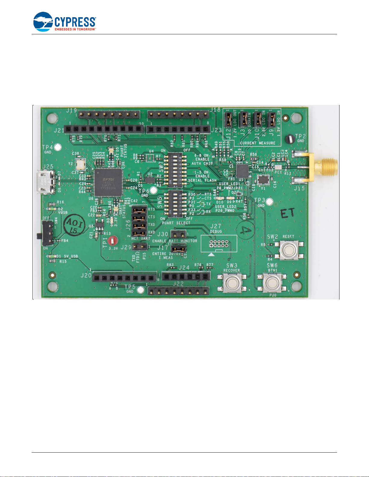
2Board Layout..................................................................................................................................................................7
3Board Block Diagram....................................................................................................................................................8
4Jumper and DIP Switch Settings..................................................................................................................................9
5Current Consumption Measurement..........................................................................................................................11
6Schematics...................................................................................................................................................................12
7CYW20706 Interfaces ..................................................................................................................................................16
7.1 Fixed Interfaces...................................................................................................................................................16
7.2 Selectable Interfaces...........................................................................................................................................17
7.3 Selectable Interfaces Supported by CYW920706WCDEVAL..............................................................................17
8GPIO Information.........................................................................................................................................................21
8.1 GPIO_Pxx............................................................................................................................................................21
8.1.1 Multiplexed GPIO_Pxx Interface Summary.............................................................................................22
8.1.2 Digital I/O Pin Interface Mapping............................................................................................................25
8.2 LHL GPIO Capabilities.........................................................................................................................................28
9Interface Signal Function Selection Restrictions and Considerations...................................................................29
9.1 I2S and PCM........................................................................................................................................................29
9.2 Serial Peripheral Interfaces .................................................................................................................................29
9.2.1 SPI1........................................................................................................................................................30
9.2.1.1 SPI1 Master..............................................................................................................................30
9.2.1.2 SPI1 Slave................................................................................................................................31
9.2.2 SPI2........................................................................................................................................................31
9.3 HCI UART............................................................................................................................................................31
9.3.1 SWD Debugging with the HCI UART......................................................................................................32
9.3.2 Bypassing the FTDI chip.........................................................................................................................32
9.4 Peripheral UART..................................................................................................................................................32
9.5 Broadcom Serial Control (BSC) (Compatible with I2C)........................................................................................34
9.6 NVRAM................................................................................................................................................................35
10 Interface Programming Information and Examples..................................................................................................36
10.1 GPIO Programming Example..............................................................................................................................36
10.2 SPI1 Master Programming Example....................................................................................................................38
10.3 SPI1 Slave Programming Example......................................................................................................................39
10.4 BSC Programming Example................................................................................................................................40
10.5 PUART Programming Example...........................................................................................................................41
10.6 NVRAM Programming Example ..........................................................................................................................42
Appendix A. Power-Save Options.............................................................................................................................43

Contents
CYW920706WCDEVAL Hardware User Guide Doc. No.: 002-16535 Rev. ** 3
A.1 Low Power Sleep Mode.......................................................................................................................................43
A.2 Deep Sleep Power Save Mode............................................................................................................................43
References............................................................................................................................................................................46
Document Revision History ................................................................................................................................................47
Worldwide Sales and Design Support................................................................................................................................48
Products ........................................................................................................................................................................48
PSoC® Solutions...........................................................................................................................................................48
Cypress Developer Community.....................................................................................................................................48
Technical Support..........................................................................................................................................................48

CYW920706WCDEVAL Hardware User Guide Doc. No.: 002-16535 Rev. ** 4
About This Document
Purpose and Audience
This document describes the Cypress Wireless Internet Connectivity for Embedded Devices (WICED; pronounced "wick-ed")
CYW920706WCDEVAL evaluation board and provides various pins, jumpers, switches, ports, and test points to access
CYW20706 to perform development, debug, evaluation, and troubleshooting. It also identifies the full complement of
interfaces available on CYW20706 and interface-selection restrictions and consequences. In addition, it provides:
•CYW20706 interface options pertinent to the Cypress CYW920706WCDEVAL reference design
•API programming information examples for configuring various CYW20706 interfaces (SPI, I2C, peripheral UART, and
more).
This document is intended for designers and developers using CYW20706 WICED devices and the CYW920706WCDEVAL
board as a reference design for CYW20706 embedded solutions with an embedded Bluetooth (BT) stack and user-developed
applications using WICED Studio.
Scope
This document details the hardware aspects of the CYW920706WCDEVAL board and interface selection considerations for
the CYW20706 device. For more information on the CYW20706 hardware, see the CYW20706 datasheet (CYW20706
Embedded Bluetooth 4.2 SoC with MCU, Bluetooth Transceiver, and Baseband Processor [1]). For information on using the
board with WICED Studio to develop embedded custom applications, see the WICED CYW920706WCDEVAL Kit Guide [2].
Several paragraphs in the document refer the reader to WICED Studio files, variables and data structures that are not
described in
this document. For information on the variables and data structures mentioned in this document, see the WICED
Studio API documentation that is provided with WICED Studio.
Acronyms and Abbreviations
In most cases, acronyms and abbreviations are defined on first use.
For a comprehensive list of acronyms and other terms used in Cypress documents, go to www.cypress.com/glossary.
IoT Resources and Technical Support
Cypress provides a wealth of data at http://www.cypress.com/internet-things-iot to help you to select the right IoT device for
your design, and quickly and effectively integrate the device into your design. Cypress provides customer access to a wide
range of information, including technical documentation, schematic diagrams, product bill of materials, PCB layout information,
and software updates. Customers can acquire technical documentation and software from the Cypress Support Community
website (http://community.cypress.com/).

CYW920706WCDEVAL Hardware User Guide Doc. No.: 002-16535 Rev. ** 5
1 Product Description
CYW20706 is a monolithic, single chip, Bluetooth (BT) dual-mode System-on-a-Chip (SoC) that includes a baseband
processor, an ARM®Cortex™-M3 processor and an integrated transceiver. It is a fully embedded device running an
embedded BT stack with support for embedded user applications developed with WICED Studio.
The Cypress CYW920706WCDEVAL board (Figure 1-1) is an evaluation board that provides various pins, jumpers, switches,
ports, and test points to access CYW20706 to perform debug, evaluation, and troubleshooting.
Figure 1-1. CYW920706WCDEVAL Board

CYW920706WCDEVAL Hardware User Guide Doc. No.: 002-16535 Rev. ** 7
2 Board Layout
Figure 2-1 shows the location of key jumpers and switches on the CYW920706WCDEVAL board.
Figure 2-1. CYW920706WCDEVAL Evaluation Board Layout and Component Locations
Note: Jumpers which are shorted by default are identified in red.

CYW920706WCDEVAL Hardware User Guide Doc. No.: 002-16535 Rev. ** 9
4 Jumper and DIP Switch Settings
Figure 2-1 shows the location for SW5, a switch that is used to configure Peripheral UART (PUART). Settings are shown in
Table 4-1.
DIP Default State Description
1 OFF Set this switch ON to use P2 as PUART_RX
2 ON Set this switch ON to use P33 as PUART_RX
3 OFF Set this switch ON to use P0 as PUART_TX
4 ON Set this switch ON to use P31 as PUART_TX
5 OFF Set this switch ON to use P3 as PUART_CTS
6 OFF Set this switch ON to use P30 as PUART_RTS
Note: Only one of DIP switches 1 or 2 should be turned ON at once (but never both), and only one of DIP switches 3 or 4 should be turned
ON at once (but never both).
Table 4-1. SW5 DIP Switch Settings
Figure 2-1 shows the location for SW7, a switch that is used to configure serial flash and authentication IC connections.
Settings are shown in Table 4-2.
DIP Default State Description
Serial Flash
1 ON Set this switch ON to power the serial flash from VDDIO
2 ON Set this switch ON to enable the SPI MISO connection between CYW20706 and serial flash
3 ON Set this switch ON to enable the SPI MOSI connection between CYW20706 and serial flash
4 ON Set this switch ON to enable the SPI CS connection between CYW20706 and serial flash
5 ON Set this switch ON to enable the SPI CLK connection between CYW20706 and serial flash
Auth IC
6 OFF Set this switch ON to power the authentication IC from VDDIO
7 OFF Set this switch ON to enable the I
2
C SDA connection between CYW20706 and authentication IC
8 OFF Set this switch ON to enable the I
2
C SCL connection between CYW20706 and authentication IC
Table 4-2. SW7 DIP Switch Settings
Authentication IC U4 is DNI by default. If the user decides to install this, then SW7 positions 6-8 must be placed in the ON
position for proper connection. If authentication IC is not used, set these to the OFF position.
See Figure 2-1 for the jumpers and switch locations. Table 4-3 shows the CYW920706WCDEVAL board jumper and switch
settings.

Jumper and DIP Switch Settings
CYW920706WCDEVAL Hardware User Guide Doc. No.: 002-16535 Rev. ** 10
Jumper/Switch Default State Comment
J3 Shorted Short this Jumper to supply 3.3V to the IO Domain (VDDIO) of the 0270x. Also use this jumper to
measure the current consumption of the IO Domain.
J9 Shorted Input of the internal 1.2V LDO, use this jumper to measure current consumption at the input of the
1.2V LDO
J10 Shorted Input of the internal 2.5V LDO, use this jumper to measure current consumption at the input of the
2.5V LDO
J12 Shorted Output of the internal 1.2V LDO, use this jumper to measure current consumption at the output of
the 1.2V LDO
J17 Shorted Supplies power to all the power rails in the 20706, use this jumper to measure current consumption
of the entire 20706 chip.
J26 1 and 2 Shorted Connects CYW20706 BT_UART_RXD to FTDI TX
J26 3 and 4 Shorted Connects CYW20706 BT_UART_TXD to FTDI RX
J26 5 and 6 Shorted Connects CYW20706 BT_UART_CTS to FTDI RTS
J26 7 and 8 Shorted Connects CYW20706 BT_UART_RTS to FTDI CTS
J29 Open Short this jumper to connect GPIO P15 to the RX of the second FTDI com port for debugging
purposes
J30 Open Short this jumper to connect GPIO P15 to VDDIO for battery monitoring applications.
SW2 – Reset Button
SW3 – Recovery Button
SW4 3 ON Power switch positions: 1: OFF, 3: ON
SW5 See Table 4-1 Serial Flash Connections
SW6 – User button
SW7 See Table 4-2 Authentication IC Connections
Table 4-3. CYW920706WCDEVAL Board Jumper and Switch Settings
Table 4-4 shows the CYW920706WCDEVAL board headers.
Header Description
J18 CYW test header - SPI, UART
J19 CYW test header – GPIO
J20 Arduino shield connection
J21 Arduino shield connection
J22 CYW test header: GPIO, Reset, I2S, PWM
J23 Arduino shield connection
J24 Arduino shield connection
J27 10 Pin JTAG connector
Table 4-4. CYW920706WCDEVAL Board Headers

CYW920706WCDEVAL Hardware User Guide Doc. No.: 002-16535 Rev. ** 11
5 Current Consumption Measurement
Table 5-1 shows the low-power Bluetooth classic mode current measured for different sleep modes in three different
scenarios.
Mode J9 (1.2V Core + Radio) J3 (IO Domain) J9 +J3 Units
No scans enabled + sleep mode 0.114 0.084 0.198 mA
Page scan enabled + sleep mode 0.328 0.083 0.411 mA
Sniff link 1.28s, 4 attempts, 0 timeout, no scans + sleep mode 1.250 0.084 1.334 mA
Table 5-1. Low-Power Bluetooth Current
Table 5-2 lists the jumper locations for measuring current.
Note: Remove the listed jumper and measure the current across the exposed pins.
To Measure... Remove the Jumper and Measure Across...
IO Domain (VDDIO) J3
1.2V LDO input (1.2V Core + Radio) J9
2.5V LDO input (2.5V LDO + On Chip Power Amplifier) J10
1.2V LDO output (1.2V Core only) J12
Total Current consumed by CYW20706 J17
Table 5-2. Current Measurements

Schematics
CYW920706WCDEVAL Hardware User Guide Doc. No.: 002-16535 Rev. ** 12
6 Schematics
Figure 6-1. CYW920706WCDEVAL Baseband Schematic

Schematics
CYW920706WCDEVAL Hardware User Guide Doc. No.: 002-16535 Rev. ** 13
Figure 6-2. CYW920706WCDEVAL RF Schematic

Schematics
CYW920706WCDEVAL Hardware User Guide Doc. No.: 002-16535 Rev. ** 14
Figure 6-3. CYW920706WCDEVAL Power & Headers Schematic

Schematics
CYW920706WCDEVAL Hardware User Guide Doc. No.: 002-16535 Rev. ** 15
Figure 6-4. CYW920706WCDEVAL USB to UART Interface Schematic

CYW920706WCDEVAL Hardware User Guide Doc. No.: 002-16535 Rev. ** 16
7 CYW20706 Interfaces
The package CYW20706 is available in may have fewer GPIOs than the die. Some of these GPIOs are fixed function IOs
while others are reconfigurable for different interfaces. To accommodate its various applications, interface selection is
accomplished through a combination of signal routing to CYW20706 and programming using the WICED API described in later
sections.
CYW20706 interfaces are presented as two interface sets: fixed and selectable. The fixed interfaces are those with dedicated
pins and, thus, are always available. The selectable interfaces are those that a board designer chooses to use from a superset
of possible interfaces that CYW20706 supports.
See Section 7.1 “Fixed Interfaces” for more information on the fixed interfaces. See Section 7.2 “Selectable Interfaces” for
more information on the set of interfaces from which board designers can choose.
7.1 Fixed Interfaces
Table 7-1 shows the fixed straps and digital I/O interfaces of CYW20706. In contrast to the Selectable Interfaces, the fixed
interfaces of CYW20706 have dedicated pins.
Strap or Interface Purpose Signals Pins
Notes
XTAL frequency selection
1
BT_XTAL_STRAP_0
G3
F2 G3 XTAL
0 0 40 MHz
0 1 24 MHz
1 0 20 MHz
1 1 Read from
NV memory
BT_XTAL_STRAP_1
F2
Device reset
RST_N
A6 Active LOW reset input
OTP usage
BT_OTP_3P3V_ON
G2 Pull HIGH if OTP is used; otherwise, pull LOW.
HCI UART
BT_UART_RXD
F5 HCI UART receive data (or SWDIO, see 9.3.1)
BT_UART_TXD
F4 HCI UART transmit data (or SWDCLK, see
9.3.1)
BT_UART_RTS_N
F3 HCI UART request-to-send input
BT_UART_CTS_N
G4 HCI UART clear-to-send input
Serial Peripheral Interface (SPI) or I
2
C, sometimes known as
Broadcom Serial Control (BSC)1
SPI2_MISO_I2C_SCL2
D8 SPI MISO
SPI2_MOSI_I2C_SDA2
E8 SPI MOSI
SPI2_CLK
E7 SPI clock output
SPI2_CSN
D7 SPI active LOW chip select output
Table 7-1. Fixed Straps and Digital I/O Interfaces
1Use the SPI2 interface for applications where the CYW20706 firmware image is to be loaded from onboard serial flash. The SPI2
interface is sometimes referred to as Spiffy2.
2Although the SPI2_MISO_I2C_SCL and SPI2_MOSI_I2C_SDA signal names imply support for an I2C-compatible interface via pins D8
and E8, an I2C-compatible interface is not usable via these pins since the SPI signals are connected to the serial flash on this hardware.
CYW20706 does support an I2C-compatible interface (BSC interface) via pins A8 and C7 (including pull ups) or B7 and C7 (see Section
9.5 “Broadcom Serial Control”).

6BCYW20706 Interfaces
CYW920706WCDEVAL Hardware User Guide Doc. No.: 002-16535 Rev. ** 17
7.2 Selectable Interfaces
CYW20706 supports several other interfaces besides those identified in Fixed Interfaces. Although CYW20706 supports
several other interfaces, it cannot support all of its interfaces in a single hardware board design. Therefore, board designers
must select which interfaces to use in a given design.
The key limitation on the selectable interfaces is the number of available digital I/O pins. The selectable interfaces are
multiplexed to 12 digital I/O pins. The 12 digital I/O pins are: A8, B5, B6, B7, C5, C6, C7, C8, D6, F7, F8, and G8.
The following interfaces represent the superset of interfaces supported by CYW20706:
Multiple general purpose I/Os (GPIOs), identified as GPIO_Pxx, and also referred to as the low leakage LHL3 GPIOs
(LHL is a low leakage power island for GPIOs on the chip). For more information on GPIO signals, see Section 8 “GPIO
Information”.
Four PWM outputs
A peripheral UART (or PUART). This PUART is for attachment to microcontroller units (MCUs) or onboard peripherals.
A Serial Peripheral Interface (SPI). This is a second SPI interface that is identified as SPI1 (and sometimes called
Spiffy1). It can be a master or a slave.
Multiple A/D converter inputs
Multiple auxiliary clock outputs
An infrared learning (IR_RX) input and playback (IR_TX) output
A keyboard scan output (KSO3)
Four optical control outputs (QOC0 through QOC3) for use in quadrature or rotary encoders.\
A 60 Hz input (60Hz_main) to a zero-crossing detector
Two triac control outputs
Two external Transmit/Receive (T/R) switch control outputs (TX_PD and ~TX_PD)
Multiple inputs from quadrature detectors (QDX0, QDX1, QDY0, QDY1, QDZ0, and QDZ1)
A shared PCM or I2S interface
A Bluetooth clock request (BT_CLK_REQ) for a shared-clock application
A Low Power Oscillator (LPO) input
An Inter-Integrated Circuit (I2C) serial interface, also called Broadcom Serial Control (BSC) interface
These selectable interfaces are mapped to the 12 digital I/O pins. Many signal functions are supported at each pin, but a
system designer must select a single function per pin. See Section 8 “GPIO Information” for detailed information on signal-
function to I/O pin assignments.
7.3 Selectable Interfaces Supported by CYW920706WCDEVAL
The CYW920706WCDEVAL board supports all of the fixed interfaces (see Section 7.1 ”Fixed Interfaces”) but only supports a
subset of the selectable interfaces (see Section 7.2 “Selectable Interfaces”) supported by CYW20706.
The CYW920706WCDEVAL board supports the following selectable interfaces:
SPI1 master
PUART
I2S, I2C, PWM, PCM
BT_GPIO_P5/P15 connected via jumper to VDDIO which can be used for voltage detect
BT_GPIO_P4/P6 to control external LEDs
BT_GPIO_P7 to monitor SW6 button depression

6BCYW20706 Interfaces
CYW920706WCDEVAL Hardware User Guide Doc. No.: 002-16535 Rev. ** 18
Table 7-2 shows which of the selectable CYW20706 interfaces are supported on the CYW920706WCDEVAL board.
CYW20706
Pin Schematic Signal Name Bonded
GPIOs
Description
Default
State I/O Type Signal Function and Notes
A8 I2S_PCM_OUT/P3/P29/P35 I2S_PCM_OUT LOW3O I2S_DO/PCM_OUT. To use I2S, set SW5-5 to the OFF position, from the SDK you need to configure
the pcm_config structure pointer with the mode role set and use the function
wiced_hal_set_pcm_config to select the I2S function. I/Os P3, P29, and P35 must remain disabled.
This pin can be configured as I2C SCL by calling
wiced_hal_i2c_init(WICED_I2C_SDA_I2S_DOUT_PCM_OUT_SCL_I2S_DIN_PCM_IN) which
selects the I2C_SCL on I2S_PCM_OUT.
P3 Floating I/O This can be used as PUART_CTS by setting SW5-5 to the ON position. It can be monitored at J22-8
if the I2S/PCM function is deselected, and I/Os P29 and P35 are disabled.
P29 Floating I/O No specific function defined. It can be monitored at J22-8 if the I2S/PCM function is deselected, and
I/Os P3 and P35 are disabled.
P35 Floating I/O No specific function defined. It can be monitored at J22-8 if the I
2
S/PCM function is deselected, and
P3 and P29 are I/O disabled. This pin can be configured as I2C SDA by calling
wiced_hal_i2c_init(WICED_I2C_SDA_P35_SCL_P37) which selects the I2C_SDA on P35
B5 BT_GPIO_5/P15 BT_GPIO_5 HIGH3I/O General Purpose I/O
P15 Floating O GPIO to monitor battery or general-purpose I/O
B6 BT_GPIO_6/P11/P26 BT_GPIO_6 LOW
3
I/O General Purpose I/O
P11 Floating I/O No specific function defined. It can be monitored at J22-4 if I/O P26 is disabled.
P26 Floating O LED D10 on/off control that can sink 16 mA and be modulated using the PWM0 circuit on
CYW20706. To use, disable I/O P11.
B7 I2S_PCM_CLK/P2/P28/P37 I2S_PCM_CLK LOW3O I2S_CLK. To use, set SW5-1 to the OFF position, select the I2S function, and disable I/Os P2, P28,
and P37.
P2 Floating I/O PUART_RX. To use, set SW5-1 to the ON position, SW5-2 to the OFF position, and
disable I/Os P28 and P37. It can be monitored at J22-5 if the I2S/PCM function is deselected with the
mentioned SW5 settings.
P28 Floating I/O No specific function defined. It can be monitored at J22-5 if the I
2
S/PCM function is deselected, and
I/Os P2 and P37 are disabled.
3CYW20706 has an internal 40K pull down for LOW state and 40K pull up for HIGH state. If the pin needs to be driven to the opposite HIGH state for an application, one of the other connected
GPIOs should be configured to drive it as needed.

6BCYW20706 Interfaces
CYW920706WCDEVAL Hardware User Guide Doc. No.: 002-16535 Rev. ** 19
CYW20706
Pin Schematic Signal Name Bonded
GPIOs
Description
Default
State I/O Type Signal Function and Notes
P37 Floating I/O No specific function defined. It can be monitored at J22-5 if the I2S/PCM function is deselected, and
I/Os P2 and P28 are disabled. This pin can be configured as I2C SCL by configuring
wiced_hal_i2c_init(WICED_I2C_SDA_P35_SCL_P37) which selects the I2C_SCL on P37
C5 BT_GPIO_3/P27/P33 BT_GPIO_3 LOW3I/O General Purpose I/O
P27 Floating O (master)
I (slave) SPI1_MOSI (master or slave)
To use, set SW5-2 to the OFF position and disable I/O P33.
P33 Floating I PUART_RX. To use, set SW5-1 to the OFF position, SW5-2 to the ON position, and disable I/O P27.
C6 BT_GPIO_7/P30 BT_GPIO_7 LOW3I/O General Purpose I/O
P30 Floating I SW6 button input. This can also be configured as PUART_RTS by setting SW5-6 to the ON position
since it is internally muxed on the same pin.
C7 I2S_PCM_IN/P12 I2S_PCM_IN LOW3I I2S_DI. To use, select the I2S function, and disable I/O P12. This pin can be configured as I2C_SDA
by calling wiced_hal_i2c_init(WICED_I2C_SDA_I2S_DOUT_PCM_OUT_SCL_I2S_DIN_PCM_IN)
which selects the I2C_SDA on I2S_PCM_IN.
P12 Floating I/O No specific function defined. It can be monitored at J22-7 if the I2S/PCM function is deselected.
C8 I2S_WS_PCM_SYNC/P0/P34 I2S_WS_PCM_SYNC LOW
3
I/O I2S_WS. To use, set SW5-3 to the OFF position, select the I
2
S function, and disable I/Os P0 and
P34.
P0 Floating I/O PUART_TX. To use, set SW5-3 to the ON position, SW5-4 to the OFF position, and
disable I/O P34. It can be monitored at J22-6 if the I2S/PCM function is deselected and I/O P34 is
disabled.
P34 Floating I/O No specific function defined. It can be monitored at J22-6 if the I2S/PCM function is deselected and
I/O P0 is disabled.
D6 BT_GPIO_4/P6/LPO_IN/P31 BT_GPIO_4 HIGH3I/O General Purpose I/O
P6 Floating I/O LED D9 on/off control that can be modulated using the PWM2 circuit on CYW20706. To use, disable
I/O P31.
P31 Floating O PUART_TX. To use, set SW5-3 to the OFF position, set SW5-4 to the ON position, and disable I/O
P6.
F7 BT_HOST_WAKE/P25/P32 BT_HOST_WAKE LOW
3
O A signal from CYW20706 device to the host indicating that the Bluetooth device requires attention
Table of contents