7
5. DESCRIPTION OF THE CIRCUIT OPERATION
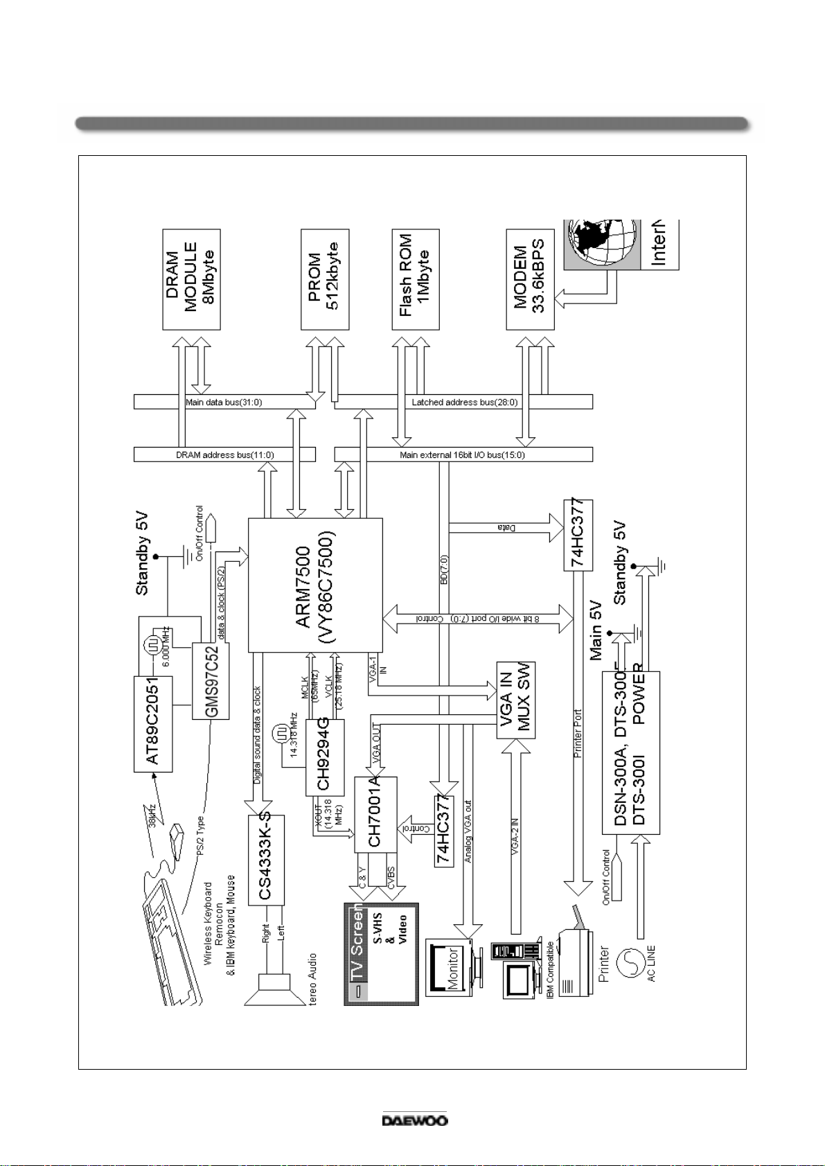
1. ARM 7500 part
The circuit is divided into digital and analogue input/output parts around the ARM 7500 part.
Two addresses and two data buses are basically served from the ARM 7500 part.
RA (DRAM ROW/COLUMN MULTIPLEXED ADDRESSES) uses 12 bits.
LA (LATCHED ADDRESSES) uses 29 bits.
D (MAIN DATA BUS) uses 32 bits.
BD (MAIN EXTERNAL BUS) uses 16 bits.
RA and D are connected to the DRAM (the capacity is 8 Mbyte), the main memory,
in the SIMM module, and are used when the actual program is operated.
2. PROM part
D and LA are connected to the PROM (the capacity is 4 Mbit).
When the power is turned on, the system reads the initial program codes set in the PROM
and loads them onto the memory.
There is a smallWEB BROWSER for emergency use in the PROM.
This can be used if there are any problems in the WEB BROWSER.
The ROM can be loaded by operating the power SW and the A/S SW.
(Turn the power SW on while pressing the A/S SW, then turn the A/S SW off in 2 sec.)
3. FLASH MEMORY part
BD and LA are connected to FLASH MEMORY (the capacity is 1 Mbyte to 4 Mbitmemories-[1 byte = 8 bit]),
which performs the same function as a hard disc in a PC.
The main program, WEB BROWSER, is loaded, and the INTERNET SET TOP BOX operates.
4. RECEIVER CIRCUIT part
A PS/2-type keyboard and a PS/2-type mouse used for PCs are provided from the ARM 7500.
These can be connected as normal-type wired keyboards and mouses or can be used as
wireless-type accessories through the receiver circuit composed of wireless receiver devices,
89C2051 and 97C52.
5. PRINTER OUTPUT part
8 bit data is supplied to the printer port from BD through 74HC377 for printing.
The printer controlsignals are supplied through the 8 bit WIDE IO PORT.
6. IMAGE OUTPUT part
VGA signals are provided to display images directly to the PC monitor from the ARM 7500.
The composite video and S-VHS(Y, C) signals are provided so that the signals can be displayed on
the CRT using the CH7001A NTSC ENCODER.
Horizontal/vertical position change: UP(26), DOWN (27), LEFT (28), RIGHT (29)
NTSC/PAL selection:NTSC*PAL (30)
Flicker filtering: MS0 (11), MS1(12)