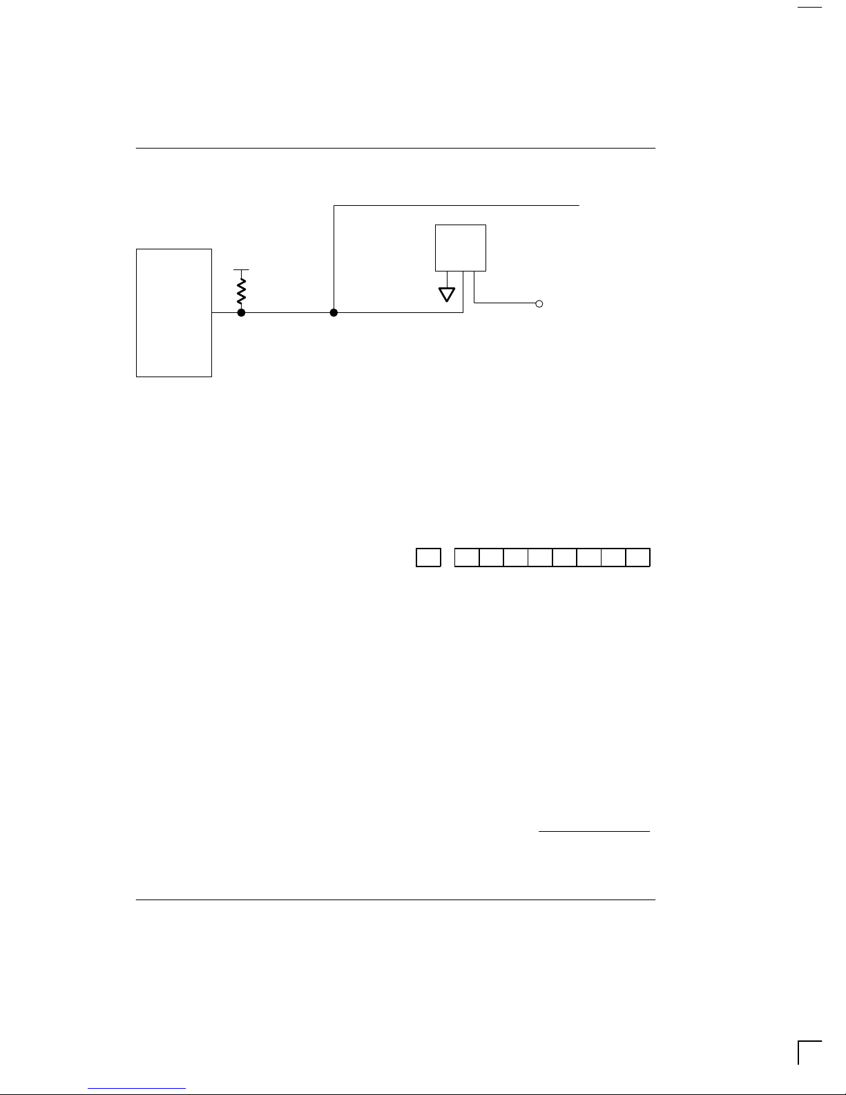
Dallas DS1820 User manual

Copyright 1995 by Dallas Semiconductor Corporation.
All Rights Reserved. For important information regarding
patents and other intellectual property rights, please refer to
Dallas Semiconductor data books.
DS1820
1–WireTM Digital Thermometer
DS1820
021497 1/27
FEATURES
•Unique1–WireTM interfacerequires onlyone portpin
for communication
•Multidropcapabilitysimplifiesdistributedtemperature
sensing applications
•Requires no external components
•Can be powered from data line
•Zero standby power required
•Measures temperatures from –55°C to +125°C in
0.5°C increments. Fahrenheit equivalent is –67°F to
+257°F in 0.9°F increments
•Temperature is read as a 9–bit digital value.
•Converts temperature to digital word in 200 ms (typ.)
•User–definable, nonvolatile temperature alarm set-
tings
•Alarm search command identifies and addresses
devices whose temperature is outside of pro-
grammed limits (temperature alarm condition)
•Applications include thermostatic controls, industrial
systems, consumer products, thermometers, or any
thermally sensitive system
PIN ASSIGNMENT
321
DALLAS
DS2434
GND
DQ
VDD
DALLAS
DS1820
321
DS1820S
16–PIN SSOP
DS1820
PR35 PACKAGE
1
2
3
4
5
6
7
8
16
15
14
13
12
11
10
9
NC
NC
NC
NC
NC
NC
NC
GND
NC
NC
NC
NC
NC
NC
VDD
DQ
BOTTOM VIEW
See Mech. Drawings
Section See Mech. Drawings
Section
PIN DESCRIPTION
GND – Ground
DQ – Data In/Out
VDD – Optional VDD
NC – No Connect
DESCRIPTION
The DS1820 Digital Thermometer provides 9–bit tem-
peraturereadingswhich indicate thetemperatureofthe
device.
Information is sent to/from the DS1820 over a 1–Wire
interface,sothatonlyonewire(andground)needstobe
connected from a central microprocessor to a DS1820.
Power for reading, writing, and performingtemperature
conversionscanbederived from thedataline itself with
no need for an external power source.
Because each DS1820 contains a unique silicon serial
number, multiple DS1820s can exist on the same
1–Wire bus. This allows for placing temperature sen-
sors in many different places. Applications where this
feature is useful include HVAC environmental controls,
sensing temperatures inside buildings, equipment or
machinery, and in process monitoring and control.

DS1820
021497 2/27
DETAILED PIN DESCRIPTION
PIN
16–PIN SSOP PIN
PR35 SYMBOL DESCRIPTION
9 1 GND Ground.
8 2 DQ Data Input/Output pin. For 1–Wire operation: Open drain. (See
“Parasite Power” section.)
7 3 VDD Optional VDD pin. See “Parasite Power” section for details of
connection.
DS1820S (16–pin SSOP): All pins not specified in this table are not to be connected.
OVERVIEW
The block diagram of Figure 1 shows the major compo-
nents of the DS1820. The DS1820 has three main data
components: 1) 64–bit lasered ROM, 2) temperature
sensor, and 3) nonvolatile temperature alarm triggers
TH and TL. The device derives its power from the
1–Wire communication line by storing energy on an
internalcapacitorduringperiodsoftimewhenthesignal
line is high and continues to operate off this power
source during the low times of the 1–Wire line until it
returnshightoreplenishtheparasite(capacitor)supply.
As an alternative, the DS1820 may also be powered
from an external 5 volts supply.
CommunicationtotheDS1820isviaa1–Wireport.With
the 1–Wire port, the memory and control functions will
not be available before the ROM function protocol has
been established. The master must first provide one of
fiveROMfunction commands: 1) Read ROM,2) Match
ROM, 3) Search ROM, 4) Skip ROM, or 5) Alarm
Search. These commands operate on the 64–bit
lasered ROM portion of each device and can single out
a specific device if many are present on the 1–Wire line
as well as indicate to the Bus Master how many and
whattypesofdevicesarepresent.AfteraROMfunction
sequencehasbeensuccessfullyexecuted,thememory
and control functions are accessible and the master
maythenprovideanyoneofthesixmemoryandcontrol
function commands.
One control function command instructs the DS1820 to
perform a temperature measurement. The result of this
measurement will be placed in the DS1820’s scratch-
pad memory, and may be read by issuing a memory
function command which reads the contents of the
scratchpad memory. The temperature alarm triggers
TH and TL consist of one byte EEPROM each. If the
alarm search command is not applied to the DS1820,
these registers may be used as general purpose user
memory. Writing TH and TL is done using a memory
function command. Read access to these registers is
through the scratchpad. All data is read and written
least significant bit first.
DS1820 BLOCK DIAGRAM Figure 1
64–BIT ROM
SCRATCHPAD
MEMORYAND
CONTROL LOGIC
AND
1–WIRE PORT TEMPERATURE SENSOR
8–BIT CRC
GENERATOR
POWER
SUPPLY
SENSE
DQ
VDD
INTERNAL VDD HIGH TEMPERATURE
TRIGGER, TH
LOW TEMPERATURE
TRIGGER, TL

+5V
+5V
DS1820
I/O
4.7K
µP
VDD
GND
DS1820
021497 3/27
PARASITE POWER
The block diagram (Figure 1) shows the parasite pow-
eredcircuitry.Thiscircuitry“steals”powerwheneverthe
I/OorVDD pinsarehigh.I/Owillprovidesufficientpower
as long as the specified timing and voltage require-
ments are met (see the section titled “1–Wire Bus Sys-
tem”). The advantages of parasite power are two–fold:
1) by parasiting off this pin, no local power source is
needed for remote sensing of temperature, and 2) the
ROM may be read in absence of normal power.
In order for the DS1820 to be able to perform accurate
temperatureconversions,sufficientpower mustbepro-
videdovertheI/Olinewhenatemperatureconversionis
takingplace.SincetheoperatingcurrentoftheDS1820
is up to 1 mA, the I/O line will not have sufficient drive
due to the 5K pull–up resistor. This problem is particu-
larly acute if several DS1820’s are on the same I/O and
attempting to convert simultaneously.
TherearetwowaystoassurethattheDS1820hassuffi-
cient supply current during its active conversion cycle.
The first is to provide a strong pull–up on the I/O line
whenever temperature conversions or copies to the E2
memoryaretakingplace.Thismaybeaccomplishedby
usingaMOSFETtopulltheI/Olinedirectlytothepower
supply as shown in Figure 2. The I/O line must be
switched over to the strong pull–up within 10 µs maxi-
mum after issuing any protocol that involves copying to
the E2memory or initiates temperature conversions.
Whenusingtheparasitepower mode, the VDD pinmust
be tied to ground.
Another method of supplying current to the DS1820 is
through the use of an external power supply tied to the
VDD pin, as shown in Figure 3. The advantage to this is
thatthestrongpull–upisnotrequiredontheI/Oline,and
thebusmasterneed notbetiedupholdingthatline high
duringtemperatureconversions.This allows other data
traffic on the 1–Wire bus during the conversion time. In
addition,anynumberofDS1820’smaybeplacedonthe
1–Wirebus,andif they alluseexternalpower, they may
allsimultaneously perform temperatureconversions by
issuing the Skip ROM command and then issuing the
Convert T command. Note that as long as the external
powersupplyisactive,theGNDpinmaynotbefloating.
The use of parasite power is not recommended above
100°C, since it may not be able to sustain communica-
tions given the higher leakage currents the DS1820
exhibits at these temperatures. For applications in
whichsuchtemperatures are likely,itis strongly recom-
mended that VDD be applied to the DS1820.
For situations where the bus master does not know
whether the DS1820’s on the bus are parasite powered
orsuppliedwithexternal VDD,aprovisionismadeinthe
DS1820 to signal the power supply scheme used. The
bus master can determine if any DS1820’s are on the
bus which require the strong pull–up by sending a Skip
ROMprotocol,thenissuingthereadpowersupplycom-
mand. After this command is issued, the master then
issues read time slots. The DS1820 will send back “0”
on the 1–Wire bus if it is parasite powered; it will send
backa“1” if itispowered from the VDD pin. If the master
receives a “0”, it knows that it must supply the strong
pull–up on the I/O line during temperature conversions.
See “Memory Command Functions” section for more
detail on this command protocol.
STRONG PULL–UP FOR SUPPLYING DS1820 DURING TEMPERATURE CONVERSION Figure 2

DS1820
021497 4/27
USING VDD TO SUPPLY TEMPERATURE CONVERSION CURRENT Figure 3
+5V
DS1820
I/O
4.7K
µPVDD
TO OTHER 1–WIRE
DEVICES
EXTERNAL +5V SUPPLY
OPERATION – MEASURING TEMPERATURE
The DS1820 measures temperature through the use of
an on–board proprietary temperature measurement
technique. A block diagram of the temperature mea-
surement circuitry is shown in Figure 4.
The DS1820 measures temperature by counting the
numberofclockcycles that anoscillator with alow tem-
perature coefficient goes through during a gate period
determined by a high temperature coefficient oscillator.
The counter is preset with a base count that corre-
spondsto–55°C.Ifthecounterreacheszerobeforethe
gate period is over, the temperature register, which is
also preset to the –55°C value, is incremented, indicat-
ing that the temperature is higher than –55°C.
Atthesametime,the counteristhenpresetwithavalue
determined by the slope accumulator circuitry. This cir-
cuitryisneededto compensatefortheparabolicbehav-
ior of the oscillators over temperature. The counter is
then clocked again until it reaches zero. If the gate
period is still not finished, then this process repeats.
The slope accumulator is used to compensate for the
non–linearbehavioroftheoscillatorsovertemperature,
yielding a high resolution temperature measurement.
This is done by changing the number of counts neces-
sary for the counter to go through for each incremental
degreein temperature.Toobtainthedesiredresolution,
therefore,boththe valueof the counter and thenumber
of counts per degree C (the value of the slope accumu-
lator) at a given temperature must be known.
Internally, this calculation is done inside the DS1820 to
provide 0.5°C resolution. The temperature reading is
provided in a 16–bit, sign–extended two’s complement
reading.Table1describesthe exact relationship ofout-
put data to measured temperature. The data is trans-
mitted serially over the 1–Wire interface. The DS1820
can measure temperature over the range of –55°C to
+125°C in 0.5°C increments. For Fahrenheit usage, a
lookup table or conversion factor must be used.
Note that temperature is represented in the DS1820 in
termsofa1/2°CLSB,yieldingthefollowing9–bitformat:
MSB LSB
1 1 1 0 0 1 1 1 0
= –25°C
Themostsignificant(sign)bit isduplicatedintoallofthe
bits in the upper MSB of the two–byte temperature reg-
ister in memory. This “sign–extension” yields the 16–bit
temperature readings as shown in Table 1.
Higher resolutions may be obtained by the following
procedure. First, read the temperature, and truncate
the0.5°Cbit(theLSB)fromthereadvalue.Thisvalueis
TEMP_READ.Thevalueleftinthecountermaythenbe
read. This value is the count remaining
(COUNT_REMAIN) after the gate period has ceased.
The last value needed is the number of counts per
degree C (COUNT_PER_C) at that temperature. The
actual temperature may be then be calculated by the
user using the following:
TEMPERATURE = TEMP_READ – 0.25
(COUNT_PER_C – COUNT_REMAIN)
COUNT_PER_C

DS1820
021497 5/27
TEMPERATURE MEASURING CIRCUITRY Figure 4
SLOPE ACCUMULATOR
PRESET
PRESET
COUNTER
COUNTER
=0
=0 STOP
INC
COMPARE
TEMPERATURE REGISTER
LOW TEMPERATURE
COEFFICIENT OSCILLATOR
HIGH TEMPERATURE
COEFFICIENT OSCILLATOR
SET/CLEAR
LSB
TEMPERATURE/DATA RELATIONSHIPS Table 1
TEMPERATURE DIGITAL OUTPUT
(Binary) DIGITAL OUTPUT
(Hex)
+125°C00000000 11111010 00FA
+25°C00000000 00110010 0032h
+1/2°C00000000 00000001 0001h
+0°C 00000000 00000000 0000h
–1/2°C11111111 11111111 FFFFh
–25°C11111111 11001110 FFCEh
–55°C11111111 10010010 FF92h
OPERATION – ALARM SIGNALING
AftertheDS1820hasperformed atemperatureconver-
sion, the temperature value is compared to the trigger
values stored in TH and TL. Since these registers are
8–bit only, the 0.5°C bit is ignored for comparison. The
most significant bit of TH or TL directly corresponds to
the sign bit of the 16–bit temperature register. If the
result of a temperature measurement is higher than TH
or lower than TL, an alarm flag inside the device is set.
This flag is updated with every temperature measure-
ment. As long as the alarm flag is set, the DS1820 will
respond to the alarm search command. This allows
manyDS1820sto be connected in paralleldoing simul-
taneoustemperaturemeasurements. Ifsomewherethe
temperature exceeds the limits, the alarming device(s)
canbeidentifiedandreadimmediatelywithouthavingto
read non–alarming devices.

DS1820
021497 6/27
64–BIT LASERED ROM
Each DS1820 contains a unique ROM code that is
64–bits long. The first eight bits are a 1–Wire family
code (DS1820 code is 10h). The next 48 bits are a
unique serial number. The last eight bits are a CRC of
the first 56 bits. (See Figure 5.) The 64–bit ROM and
ROM Function Control section allow the DS1820 to
operateasa1–Wiredeviceandfollowthe1–Wireproto-
col detailed in the section “1–Wire Bus System”. The
functionsrequiredtocontrolsectionsoftheDS1820are
notaccessibleuntiltheROMfunctionprotocolhasbeen
satisfied.ThisprotocolisdescribedintheROMfunction
protocol flowchart (Figure 6). The 1–Wire bus master
must first provide one of five ROM function commands:
1) Read ROM, 2) Match ROM, 3) Search ROM, 4) Skip
ROM, or 5) Alarm Search. After a ROM functions
sequence has been successfully executed, the func-
tionsspecifictothe DS1820 are accessibleand the bus
mastermaythenprovideandoneofthesixmemoryand
control function commands.
CRC GENERATION
TheDS1820hasan8–bitCRCstoredinthemostsignif-
icantbyte of the 64–bit ROM.The busmaster can com-
pute a CRC value from the first 56–bits of the 64–bit
ROM and compare it to the value stored within the
DS1820 to determine if the ROM data has been
received error–free by the bus master. The equivalent
polynomial function of this CRC is:
CRC = X8+ X5+ X4+ 1
The DS1820 also generates an 8–bit CRC value using
the same polynomial function shown above and pro-
videsthisvaluetothebusmastertovalidatethetransfer
ofdatabytes.IneachcasewhereaCRCisusedfordata
transfer validation, the bus master must calculate a
CRC value using the polynomial function given above
and compare the calculated value to either the 8–bit
CRC value stored in the 64–bit ROM portion of the
DS1820 (for ROM reads) or the 8–bit CRC value com-
puted within the DS1820 (which is read as a ninth byte
when the scratchpad is read). The comparison of CRC
values and decision to continue with an operation are
determined entirely by the bus master. There is no cir-
cuitry inside the DS1820 that prevents a command
sequencefromproceedingiftheCRCstoredinorcalcu-
lated by the DS1820 does not match the value gener-
ated by the bus master.
The 1–Wire CRC can be generated using a polynomial
generator consisting of a shift register and XOR gates
as shown in Figure 7. Additional information about the
Dallas1–WireCyclicRedundancyCheckisavailablein
Application Note 27 entitled “Understanding and Using
CyclicRedundancy Checks withDallas Semiconductor
Touch Memory Products”.
The shift register bits are initialized to zero. Then start-
ingwiththeleastsignificantbitofthefamilycode,onebit
at a time is shifted in. After the 8th bit of the family code
has been entered, then the serial number is entered.
Afterthe48thbitofthe serialnumberhasbeenentered,
theshift register containsthe CRC value. Shifting inthe
eight bits of CRC should return the shift register to all
zeros.
64–BIT LASERED ROM Figure 5
8–BIT CRC CODE 48–BIT SERIAL NUMBER 8–BIT FAMILY CODE (10h)
MSB LSB MSB LSB MSB LSB

N
Y
Y
Y
DS1820 TX
PRESENCE
PULSE
33h
READ ROM
COMMAND
55h
MATCH ROM
COMMAND
F0h
SEARCH ROM
COMMAND
CCh
SKIP ROM
COMMAND
DS1820 TXFAMILY
CODE
1 BYTE
BIT 0
MATCH? BIT 0
MATCH?
BIT 1
MATCH? BIT 1
MATCH?
BIT 63
MATCH? BIT 63
MATCH?
DS1820 TX
SERIAL NUMBER
6 BYTES
DS1820 TX
CRC BYTE
NNN
YYY
NN
Y
N
N
Y
YY
DS1820 TXBIT 0
DS1820 TXBIT 0
DS1820 TXBIT 1
DS1820 TXBIT 1
DS1820 TXBIT 63
DS1820 TXBIT 63
MASTER TXBIT 1
MASTER TXBIT 0
MASTER TXBIT 0
MASTER TXBIT 1
MASTER TXBIT 63
MASTER TXBIT 63
MASTER TX
RESET PULSE
MASTER TXROM
FUNCTION COMMAND
MASTER TXMEMORY OR CONTROL
FUNCTION COMMAND
NN
Y
ECh
ALARM SEARCH
COMMAND
ALARM
CONDITION
?
Y
N
N
DS1820
021497 7/27
ROM FUNCTIONS FLOW CHART Figure 6

DS1820
021497 8/27
1–WIRE CRC CODE Figure 7
(MSB) (LSB)
XOR XOR XOR
INPUT
MEMORY
The DS1820’s memory is organized as shown in
Figure 8. The memory consists of a scratchpad RAM
andanonvolatile,electricallyerasable(E2)RAM,which
storesthehighandlowtemperaturetriggersTHandTL.
The scratchpad helps insure data integrity when com-
municating over the 1–Wire bus. Data is first written to
thescratchpadwhereitcanbereadback.Afterthedata
has been verified, a copy scratchpad command will
transfer the data to the nonvolatile (E2) RAM. This pro-
cessinsuresdataintegritywhenmodifyingthememory.
The scratchpad is organized as eight bytes of memory.
The first two bytes contain the measured temperature
information. The third and fourth bytes are volatile
copies of TH and TL and are refreshed with every pow-
er–on reset. The next two bytes are not used; upon
reading back, however, they will appear as all logic 1’s.
Theseventhandeighthbytesarecountregisters,which
maybeusedinobtaininghighertemperatureresolution
(see “Operation–measuring Temperature” section).
There is a ninth byte which may be read with a Read
Scratchpad command. This byte contains a cyclic
redundancycheck(CRC)bytewhichistheCRCoverall
oftheeightpreviousbytes.ThisCRCisimplementedin
thefashiondescribedinthesectiontitled“CRCGenera-
tion”.
DS1820 MEMORY MAP Figure 8
TEMPERATURE LSB
TEMPERATURE MSB
TH/USER BYTE 1
TL/USER BYTE 2
RESERVED
RESERVED
COUNT REMAIN
CRC
BYTE
0
1
2
3
4
5
6
7
8
TH/USER BYTE 1
TL/USER BYTE 2
SCRATCHPAD E2RAM
COUNT PER °C

DS1820
021497 9/27
1–WIRE BUS SYSTEM
The1–Wirebusisasystemwhichhasasinglebusmas-
ter and one or more slaves. The DS1820 behaves as a
slave.Thediscussionofthisbussystemisbrokendown
into three topics: hardware configuration, transaction
sequence, and 1–Wire signaling (signal types and tim-
ing).
HARDWARE CONFIGURATION
The 1–Wire bus has only a single line by definition; it is
important that each device on the bus be able to drive it
at the appropriate time. To facilitate this, each device
attached to the 1–Wire bus must have open drain or
3–state outputs. The 1–Wire port of the DS1820 (I/O
pin) is open drain with an internal circuit equivalent to
that shown in Figure 9. A multidrop bus consists of a
1–Wire bus with multiple slaves attached. The 1–Wire
bus requires a pullup resistor of approximately 5KΩ.
HARDWARE CONFIGURATION Figure 9
+5V
4.7K
RX
TX
RX
TX
1OO OHM
MOSFET
DS1820 1–WIRE PORTBUS MASTER
5 µA
Typ.
RX= RECEIVE
TX= TRANSMIT
Theidlestateforthe1–Wirebusishigh.Ifforanyreason
atransactionneedstobesuspended,thebusMUST be
leftintheidlestateifthetransactionistoresume.Infinite
recovery time can occur between bits so long as the
1–Wire bus is in the inactive (high) state during the re-
covery period. If this does not occur and the bus is left
lowformorethan480µs,allcomponentsonthebuswill
be reset.
TRANSACTION SEQUENCE
The protocol for accessing the DS1820 via the 1–Wire
port is as follows:
•Initialization
•ROM Function Command
•Memory Function Command
•Transaction/Data
INITIALIZATION
All transactions on the 1–Wire bus begin with an initial-
ization sequence. The initialization sequence consists
of a reset pulse transmitted by the bus master followed
by presence pulse(s) transmitted by the slave(s).
The presence pulse lets the bus master know that the
DS1820ison thebus and is ready tooperate.Formore
details, see the “1–Wire Signaling” section.
ROM FUNCTION COMMANDS
Once the bus master has detected a presence, it can
issueoneofthefiveROMfunctioncommands.AllROM
functioncommandsare8–bits long. A listof these com-
mands follows (refer to flowchart in Figure 6):

DS1820
021497 10/27
Read ROM [33h]
This command allows the bus master to read the
DS1820’s 8–bit family code, unique 48–bit serial num-
ber, and 8–bit CRC. This command can only be used if
there is a single DS1820 on the bus. If more than one
slave is present on the bus, a data collision will occur
when all slaves try to transmit at the same time (open
drain will produce a wired AND result).
Match ROM [55h]
The match ROM command, followed by a 64–bit ROM
sequence, allows the bus master to address a specific
DS1820 on a multidrop bus. Only the DS1820 that
exactlymatchesthe64–bitROMsequencewillrespond
to the following memory function command. All slaves
thatdonotmatch the 64–bitROMsequencewillwaitfor
a reset pulse. This command can be used with a single
or multiple devices on the bus.
Skip ROM [CCh]
This command can save time in a single drop bus sys-
tem by allowing the bus master to access the memory
functions without providing the 64–bit ROM code. If
more than one slave is present on the bus and a read
command is issued following the Skip ROM command,
data collision will occur on the bus as multiple slaves
transmit simultaneously (open drain pulldowns will pro-
duce a wired AND result).
Search ROM [F0h]
When a system is initially brought up, the bus master
might not know the number of devices on the 1–Wire
bus or their 64–bit ROM codes. The search ROM com-
mandallowsthebusmastertouseaprocessofelimina-
tiontoidentifythe64–bitROMcodesofallslavedevices
on the bus.
Alarm Search [ECh]
TheflowchartofthiscommandisidenticaltotheSearch
ROM command. However, the DS1820 will respond to
this command only if an alarm condition has been
encountered at the last temperature measurement. An
alarmconditionis defined asa temperature higherthan
THorlowerthanTL. Thealarmconditionremainssetas
longastheDS1820is poweredup,oruntilanothertem-
perature measurement reveals a non–alarming value.
For alarming, the trigger values stored in EEPROM are
taken into account. If an alarm condition exists and the
TH or TL settings are changed, another temperature
conversionshouldbe done to validate anyalarm condi-
tions.
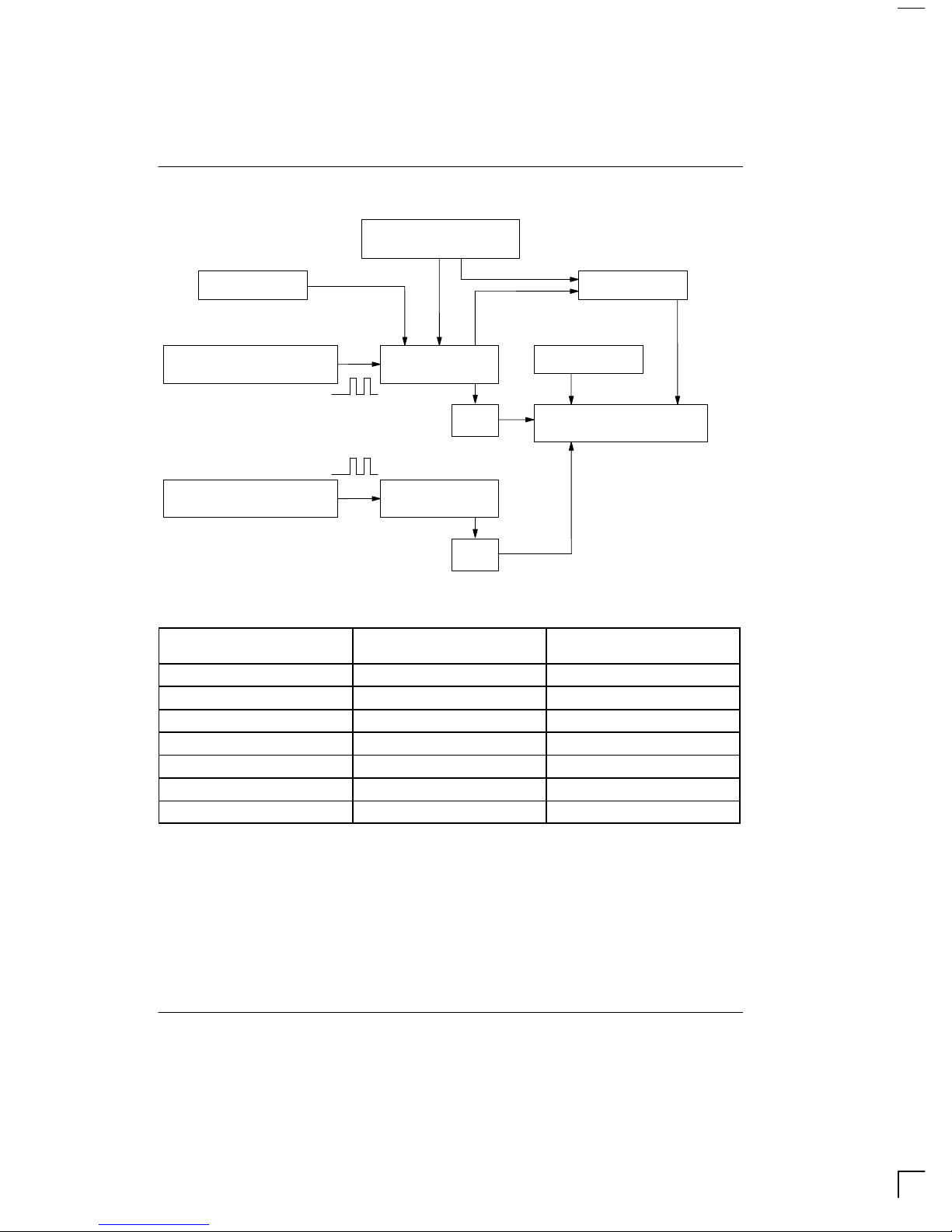
Example of a ROM Search
The ROM search process is the repetition of a simple
3–step routine: read a bit, read the complement of the
bit,thenwritethedesiredvalueofthatbit.Thebus mas-
ter performs this simple, 3–step routine on each bit of
the ROM. After one complete pass, the bus master
knows the contents of the ROM in one device. The
remainingnumberofdevicesandtheirROMcodesmay
be identified by additional passes.
The following example of the ROM search process
assumes four different devices are connected to the
same 1–Wire bus. The ROM data of the four devices is
as shown:
ROM1 00110101...
ROM2 10101010...
ROM3 11110101...
ROM4 00010001...
The search process is as follows:
1. Thebusmasterbeginstheinitializationsequenceby
issuinga reset pulse. The slavedevices respond by
issuing simultaneous presence pulses.
2. The bus master will then issue the Search ROM
command on the 1–Wire bus.
3. The bus master reads a bit from the 1–Wire bus.
Each device will respond by placing the value of the
firstbitoftheirrespectiveROMdataontothe1–Wire
bus. ROM1 and ROM4 will place a 0 onto the
1–Wire bus, i.e., pull it low. ROM2 and ROM3 will
placea 1 ontothe 1–Wire bus by allowingthe lineto
stayhigh. TheresultisthelogicalANDofalldevices
on the line, therefore the bus master sees a 0. The
bus master reads another bit. Since the Search
ROM data command is being executed, all of the
devices on the 1–Wire bus respond to this second
readbyplacingthecomplementofthefirstbitoftheir
respective ROM data onto the 1–Wire bus. ROM1
and ROM4 will place a 1 onto the 1–Wire, allowing
the line to stay high. ROM2 and ROM3 will place a
0ontothe1–Wire, thus it will bepulledlow. Thebus
masteragainobservesa0forthecomplementofthe
first ROM data bit. The bus master has determined
that there are some devices on the 1–Wire bus that
have a 0 in the first position and others that have a 1.

DS1820
021497 11/27
The data obtained from the two reads of the 3–step
routine have the following interpretations:
00 There are still devices attached which have
conflicting bits in this position.
01 All devices still coupled have a 0–bit in this
bit position.
10 All devices still coupled have a 1–bit in this
bit position.
11 Therearenodevicesattachedtothe1–Wire
bus.
4. The bus master writes a 0. This deselects ROM2
and ROM3 for the remainder of this search pass,
leaving only ROM1 and ROM4 connected to the
1–Wire bus.
5. The bus master performs two more reads and
receives a 0–bit followed by a 1–bit. This indicates
that all devices still coupled to the bus have 0’s as
their second ROM data bit.
6. The bus master then writes a 0 to keep both ROM1
and ROM4 coupled.
7. The bus master executes two reads and receives
two0–bits.Thisindicatesthatboth1–bitsand0–bits
existas the third bit ofthe ROM dataof the attached
devices.
8. Thebusmasterwritesa0–bit.ThisdeselectsROM1
leaving ROM4 as the only device still connected.
9. ThebusmasterreadstheremainderoftheROMbits
for ROM4 and continues to access the part if
desired. This completes the first pass and uniquely
identifies one part on the 1–Wire bus.
10.ThebusmasterstartsanewROMsearchsequence
by repeating steps 1 through 7.
11. The bus master writes a 1–bit. This decouples
ROM4, leaving only ROM1 still coupled.
12.ThebusmasterreadstheremainderoftheROMbits
forROM1andcommunicates totheunderlyinglogic
if desired. This completes the second ROM search
pass, in which another of the ROMs was found.
13.ThebusmasterstartsanewROMsearchbyrepeat-
ing steps 1 through 3.
14.The bus master writes a 1–bit. This deselects
ROM1 and ROM4 for the remainder of this search
pass, leaving only ROM2 and ROM3 coupled to the
system.
15.The bus master executes two read time slots and
receives two zeros.
16.The bus master writes a 0–bit. This decouples
ROM3, and leaving only ROM2.
17.ThebusmasterreadstheremainderoftheROMbits
forROM2andcommunicates totheunderlyinglogic
if desired. This completes the third ROM search
pass, in which another of the ROMs was found.
18.ThebusmasterstartsanewROMsearchbyrepeat-
ing steps 13 through 15.
19.The bus master writes a 1–bit. This decouples
ROM2, leaving only ROM3.
20.ThebusmasterreadstheremainderoftheROMbits
forROM3andcommunicates totheunderlyinglogic
if desired. This completes the fourth ROM search
pass, in which another of the ROMs was found.
Note the following:
ThebusmasterlearnstheuniqueIDnumber(ROMdata
pattern) of one 1–Wire device on each ROM Search
operation. The time required to derive the part’s unique
ROM code is:
960 µs + (8 + 3 x 64) 61 µs = 13.16 ms
Thebusmasteristhereforecapableofidentifying75dif-
ferent 1–Wire devices per second.
I/O SIGNALING
The DS1820 requires strict protocols to insure data
integrity. The protocol consists of several types of
signalingononeline:resetpulse,presencepulse,write
0, write 1, read 0, and read 1. All of these signals, with
theexception of thepresence pulse, areinitiated by the
bus master.
The initialization sequence required to begin any com-
munication with the DS1820 is shown in Figure 11. A
reset pulse followed by a presence pulse indicates the
DS1820 is ready to send or receive data given the cor-
rect ROM command and memory function command.
The bus master transmits (TX) a reset pulse (a low sig-
nal for a minimum of 480 µs). The bus master then
releases the line and goes into a receive mode (RX).
The 1–Wire bus is pulled to a high state via the 5K
pull–up resistor . After detecting the rising edge on the

DS1820
021497 12/27
I/O pin, the DS1820 waits 15–60 µs and then transmits
the presence pulse (a low signal for 60–240 µs).
MEMORY COMMAND FUNCTIONS
The following command protocols are summarized in
Table 2, and by the flowchart of Figure 10.
Write Scratchpad [4Eh]
This command writes to the scratchpad of the DS1820,
starting at address 2. The next two bytes written will be
saved in scratchpad memory, at address locations 2
and3.Writingmaybeterminatedatanypointbyissuing
a reset.

DS1820
021497 13/27
MEMORY FUNCTIONS FLOW CHART Figure 10
4Eh
WRITE
SCRATCHPAD
?
MASTER TXMEMORY
OR CONTROL COMMAND
DS1820 SETS ADDRESS
COUNTER TO 2
MASTER TXDATA BYTE
TO SCRATCHPAD
MASTER
TXRESET
?
ADDRESS
=3
?
DS1820 INCREMENTS
ADDRESS
MASTER
TXRESET
?
BEh
READ
SCRATCHPAD
?
DS1820 SETS ADDRESS
COUNTER TO 0
MASTER RXDATA
FROM SCRATCHPAD
MASTER
TXRESET
?
ADDRESS
=7
?
DS1820 INCREMENTS
ADDRESS
MASTER RX8–BIT
CRC OF DATA
DS1820 TX
PRESENCE PULSE
MASTER
TXRESET
?
MASTER RX“1s”
N N
N
N
N
N
N
N
Y
Y
Y
Y
Y
Y
Y
Y

DS1820
021497 14/27
MEMORY FUNCTIONS FLOW CHART Figure 10 (cont’d)
48h
COPY
SCRATCHPAD
?
44h
CONVERT
TEMPERATURE
?
PARASITE
POWER
?
MASTER ENABLES
STRONG PULL–UP
NN
Y
Y
Y
DS1820 CONVERTS
TEMPERATURE
MASTER DISABLES
STRONG PULL–UP
DS1820 BEGINS
CONVERSION
MASTER TX
RESET
?
DEVICE BUSY
CONVERTING
TEMPERATURE
?
MASTER
RX“1”s MASTER
RX“0”s
MASTER TX
RESET
?
NONVOLATILE
MEMORY
BUSY
?
MASTER
RX“1”s MASTER
RX“0”s
N
NY
NY
N
Y
N
Y
PARASITE
POWER
?
MASTER ENABLES
STRONG PULLUP FOR
10 ms
MASTER DISABLES
STRONG PULLUP
NY

DS1820
021497 15/27
MEMORY FUNCTIONS FLOW CHART Figure 10 (cont’d)
B8h
RECALL
E2
?
DS1820 RECALLS
FROM E2PROM
MASTER
TXRESET
?
B4h
READ
POWER SUPPLY
?
NN
Y
Y
MASTER
TXRESET
?
N
Y
Y
PARASITE
POWERED
?
MASTER
RX“0”s
NY
MASTER
RX“1”s
MASTER
TXRESET
?
N
Y
DEVICE
BUSY CONVERTING
TEMPERATURE
?
MASTER
RX“0”s
MASTER
RX“1”s
YN

DS1820
021497 16/27
INITIALIZATION PROCEDURE “RESET AND PRESENCE PULSES” Figure 11
Master TX“reset pulse”
480 µs minimum
960 µs maximum
Master RX
480 µs minimum
VCC
GND
DS1820
waits
15 - 60 µsDS1820 TX
“presence pulse”
60 - 240 µs
LINE TYPE LEGEND:
Bus master active low
Both bus master and
DS1820 active low
DS1820 active low
Resistor pull–up
1–WIRE
BUS
DS1820 COMMAND SET Table 2
INSTRUCTION DESCRIPTION PROTOCOL
1–WIRE BUS
AFTER ISSUING
PROTOCOL NOTES
TEMPERATURE CONVERSION COMMANDS
Convert T Initiates temperature conversion. 44h <read temperature
busy status> 1
MEMORY COMMANDS
Read Scratchpad Reads bytes from scratchpad and
reads CRC byte. BEh <read data up to 9
bytes>
Write Scratchpad Writes bytes into scratchpad at
addresses 2 and 3 (TH and TL
temperature triggers).
4Eh <write data into 2
bytes at addr. 2 and
addr. 3>
Copy Scratchpad Copies scratchpad into nonvolatile
memory (addresses 2 and 3 only). 48h <read copy status> 2
Recall E2Recalls values stored in nonvolatile
memory into scratchpad (tempera-
ture triggers).
B8h <read temperature
busy status>
Read Power Supply Signals the mode of DS1820
power supply to the master. B4h <read supply status>
NOTES:
1. Temperature conversion takes up to 500 ms. After receiving the Convert T protocol, if the part does not
receive power from the VDD pin, the I/O line for the DS1820 must be held high for at least 500 ms to provide
power during the conversion process. As such, no other activity may take place on the 1–Wire bus for at least
this period after a Convert T command has been issued.
2. After receiving the Copy Scratchpad protocol, if the part does not receive power from the VDD pin, the I/O line
for the DS1820 must be held high for at least 10 ms to provide power during the copy process. As such, no
other activity may take place on the 1–Wire bus for at least this period after a Copy Scratchpad command has
been issued.

DS1820
021497 17/27
Read Scratchpad [BEh]
This command reads the contents of the scratchpad.
Reading will commence at byte 0, and will continue
throughthescratchpaduntilthe9th (byte–8, CRC) byte
isread.Ifnotalllocationsaretoberead,themastermay
issue a reset to terminate reading at any time.
Copy Scratchpad [48h]
This command copies the scratchpad into the E2
memory of the DS1820, storing the temperature trigger
bytes in nonvolatile memory. If the bus master issues
readtimeslotsfollowingthiscommand,theDS1820will
output “0” on the bus as long as it is busy copying the
scratchpad to E2; it will return a “1” when the copy pro-
cess is complete. If parasite powered, the bus master
hastoenableastrongpull–upforatleast10msimmedi-
ately after issuing this command.
Convert T [44h]
This command begins a temperature conversion. No
furtherdataisrequired.Thetemperatureconversionwill
be performed and then the DS1820 will remain idle. If
thebusmasterissuesreadtimeslotsfollowingthiscom-
mand,theDS1820willoutput“0”onthebusaslongasit
isbusymakingatemperatureconversion;it will returna
“1”whenthetemperatureconversioniscomplete.Ifpar-
asite powered, the bus master has to enable a strong
pullup for 500 ms immediately after issuing this com-
mand.
Recall E2 [B8h]
This command recalls the temperature trigger values
storedinE2tothescratchpad.Thisrecalloperationhap-
pens automatically upon power–up to the DS1820 as
well,sovaliddata is availableinthescratchpadassoon
as the device has power applied. With every read data
time slot issued after this command has been sent, the
device will output its temperature converter busy flag
“0”=busy, “1”=ready.
Read Power Supply [B4h]
With every read data time slot issued after this com-
mand has been sent to the DS1820, the device will sig-
nal its power mode: “0”=parasite power, “1”=external
power supply provided.
READ/WRITE TIME SLOTS
DS1820dataisread andwrittenthroughtheuseoftime
slotstomanipulate bits and acommand word to specify
the transaction.
Write Time Slots
A write time slot is initiated when the host pulls the data
linefromahigh logic levelto a lowlogiclevel. There are
two types of write time slots: Write One time slots and
WriteZero time slots. All write time slots must be a mini-
mum of 60 µs in duration with a minimum of a one µs
recovery time between individual write cycles.
TheDS1820samplestheI/Olineinawindowof15µsto
60µsaftertheI/Olinefalls.Ifthelineishigh,aWriteOne
occurs. If the line is low, a Write Zero occurs (see
Figure 12).
For the host to generate a Write One time slot, the data
linemustbepulledtoalogiclowlevelandthenreleased,
allowing the data line to pull up to a high level within
15 µs after the start of the write time slot.
Forthe host to generate a WriteZero time slot, the data
linemustbepulledtoalogiclowlevelandremainlowfor
60 µs.
Read Time Slots
The host generates read time slots when data is to be
readfromtheDS1820.Areadtimeslotisinitiatedwhen
thehostpullsthedatalinefromalogichigh leveltologic
low level. The data line must remain at a low logic level
foraminimumofoneµs;outputdatafromtheDS1820is
validfor15 µsafterthefallingedgeofthereadtimeslot.
The host therefore must stop driving the I/O pin low in
ordertoreaditsstate15 µsfromthestartofthereadslot
(seeFigure 12). Bythe end ofthe read time slot, theI/O
pinwillpullbackhighviatheexternalpull–upresistor.All
read time slots must be a minimum of 60 µs in duration
withaminimumofaone µs recovery time between indi-
vidual read slots.
Figure 13 shows that the sum of TINIT, TRC, and
TSAMPLE mustbeless than 15µs. Figure 14 showsthat
system timing margin is maximized by keeping TINIT
andTRCassmallaspossibleandbylocatingthemaster
sample time towards the end of the 15 µs period.

DS1820
021497 18/27
READ/WRITE TIMING DIAGRAM Figure 12
1–WIRE
BUS
MASTER WRITE “0” SLOT MASTER WRITE “1” SLOT
60 µs<TX“0”<120 µs
>1 µs
15 µs30 µs15 µs 30 µs
DS1820 SAMPLES
MIN TYP MAX
MASTER READ “0” SLOT MASTER READ “1” SLOT
15 µs
>1 µs
MASTER SAMPLES
15 µs 15 µs
DS1820 SAMPLES
MIN TYP MAX
1 µs< tREC <∞
1 µs< tREC <∞
15 µs30 µs15 µs
MASTER SAMPLES
LINE TYPE LEGEND:
Bus master active low
Both bus master and
DS1820 active low
DS1820 active low
Resistor pull–up
VCC
GND
ÇÇÇ
ÇÇÇ
ÇÇÇ
1–WIRE
BUS
ÇÇÇÇÇÇÇÇ
ÇÇÇÇÇÇÇÇ
ÇÇÇÇÇÇÇÇ
VCC
GND
ÇÇÇ
ÇÇÇ
ÇÇÇ

DS1820
021497 19/27
DETAILED MASTER READ “1” TIMING Figure 13
VCC
GND
15 µs
TINIT>1 µS TRC MASTER SAMPLES
1–WIRE
BUS VIH OF MASTER
RECOMMENDED MASTER READ “1” TIMING Figure 14
VCC
GND
15 µs
MASTER
SAMPLES
TRC =
SMALL
TINIT =
SMALL
1–WIRE
BUS VIH OF MASTER
LINE TYPE LEGEND:
Bus master active low
Both bus master and
DS1820 active low
DS1820 active low
Resistor pull–up

DS1820
021497 20/27
Related Application Notes
The following Application Notes can be applied to the
DS1820. These notes can be obtained from the Dallas
Semiconductor “Application Note Book”, via our web-
siteat http://www.dalsemi.com/,orthrough our faxback
service at (214) 450–0441.
Application Note 27: “Understanding and Using Cyclic Redundancy Checks with Dallas Semiconductor Touch
Memory Product”
Application Note 55: “Extending the Contact Range of Touch Memories”
Application Note 74: “Reading and Writing Touch Memories via Serial Interfaces”
Application Note 104: “Minimalist Temperature Control Demo”
Application Note 105: “High Resolution Temperature Measurement with Dallas Direct–to–Direct Temperature Sen-
sors”
Application Note 106: “Complex MicroLANs”
Application Note 108: “MicroLAN – In the Long Run”
Sample 1–Wire subroutines that can be used in conjunction with AN74 can be downloaded from the website or our
Anonymous FTP Site.
Table of contents