Delta Tau PMAC2 VME Ultralite Quick user guide

^1 HARDWARE REFERENCE MANUAL
^2 PMAC2 VME Ultralite
^3 VME Ultralite Control Board
^4 3xx-602643-xHxx
^5 June 1997
Single Source Machine Control Power // Flexibility // Ease of Use
21314 Lassen Street Chatsworth, CA 91311 // Tel. (818) 998-2095 Fax. (818) 998-7807 // www.deltatau.com

Copyright Information
© 2003 Delta Tau Data Systems, Inc. All rights reserved.
This document is furnished for the customers of Delta Tau Data Systems, Inc. Other uses are
unauthorized without written permission of Delta Tau Data Systems, Inc. Information contained in
this manual may be updated from time-to-time due to product improvements, etc., and may not
conform in every respect to former issues.
To report errors or inconsistencies, call or email:
Delta Tau Data Systems, Inc. Technical Support
Phone: (818) 717-5656
Fax: (818) 998-7807
Email: [email protected]
Website: http://www.deltatau.com
Operating Conditions
All Delta Tau Data Systems, Inc. motion controller products, accessories, and amplifiers contain
static sensitive components that can be damaged by incorrect handling. When installing or handling
Delta Tau Data Systems, Inc. products, avoid contact with highly insulated materials. Only
qualified personnel should be allowed to handle this equipment.
In the case of industrial applications, we expect our products to be protected from hazardous or
conductive materials and/or environments that could cause harm to the controller by damaging
components or causing electrical shorts. When our products are used in an industrial environment,
install them into an industrial electrical cabinet or industrial PC to protect them from excessive or
corrosive moisture, abnormal ambient temperatures, and conductive materials. If Delta Tau Data
Systems, Inc. products are exposed to hazardous or conductive materials and/or environments, we
cannot guarantee their operation.

PMAC -VME Ultralite Hardware Reference Manual
Table of Contents i
Table of Contents
INTRODUCTION.......................................................................................................................................................1
Overview...................................................................................................................................................................1
Features.....................................................................................................................................................................1
Input/Output..........................................................................................................................................................1
Firmware..............................................................................................................................................................1
DSPGATE2 I/O ASIC ..............................................................................................................................................2
CONNECTORS AND JUMPERS..............................................................................................................................3
Connector Summary..................................................................................................................................................3
J2/JTHW (26-Pin Header)....................................................................................................................................4
J3/JIO (40-Pin Header)........................................................................................................................................5
J5/JRS232 (10-Pin Header)..................................................................................................................................6
J5A/JRS422 (26-Pin Header) ...............................................................................................................................7
J6/JDISP (14-Pin Header)....................................................................................................................................8
J7/JHW (20-Pin Header)......................................................................................................................................8
P1 JVME (96-Pin Header) ...................................................................................................................................9
P2 JVME (96-Pin Header) .................................................................................................................................10
TB1 (2-Pin Terminal Block) ...............................................................................................................................11
TB2 (3-Pin Terminal Block) ...............................................................................................................................11
MACRO Interface Connectors................................................................................................................................11
Version 1: Fiber Optic Transceiver....................................................................................................................11
Version 2: Coaxial Cable Connectors................................................................................................................11
Version 3: RJ-45 Phone Jack Connectors ..........................................................................................................11
Jumper Summary.....................................................................................................................................................12
E1: Card 0 Select................................................................................................................................................12
E2: 40MHz/60MHz CPU Operation...................................................................................................................12
E3: Re-Initialization On Reset Control...............................................................................................................12
E4-E6: (Reserved For Future Use).....................................................................................................................12
E7: Multi-Board Daisy-Chain Configure...........................................................................................................12
E8: RS232 Converter Power Supply Control .....................................................................................................13
E9 - E16: Serial Interface Handshake Control...................................................................................................13
E15A-H, E16A-H: DPRAM Byte Order Control................................................................................................14
E17 - E18: Serial Connector Select....................................................................................................................14
E19: Watchdog Control Jumper.........................................................................................................................14
E20-E21: DPRAM Byte Read/Write Order Control...........................................................................................14
SCHEMATICS..........................................................................................................................................................15

PMAC2 VME Ultralite Hardware Reference Manual
ii Table of Contents

PMAC -VME Ultralite Hardware Reference Manual
Introduction 1
INTRODUCTION
Overview
The PMAC2 VME Ultralite control board is a member of the PMAC2 family of controllers that replaces
the local axis interface circuitry with the MACRO ring network interface. The Ultralite name is used
because of the lack of any direct on-board axis interface circuitry. In other words, the interface hardware
for channels 1 through 8 is missing on the Ultralite.
Features
Input/Output
The Ultralite board does retain the local general purpose I/O of the PMAC family, including:
• JDISP display port
• JTHW multiplexer port
• JIO general I/O port
• JHW handwheel port
• JRS232 serial port
• JRS422 serial port
The Ultralite board’s MACRO interface is available in one of three forms; one of the three must be ordered:
• SC optical fiber interface
• BNC coaxial cable interface
• RJ-45 "phone jack" interface
The following ports are not available on the PMAC2 VME Ultralite:
• JANA analog input port
• JEQU position compare output port
• JMACHn axis interface ports
Firmware
The firmware for the Ultralite functions identically to that of other members of the PMAC2 family, which
is very similar to the firmware for the original PMAC family. Because of the hardware differences, there
are some differences in the use of the firmware.
• Variables I910 to I989, which control the setup of machine interface channels 1-8, are useless,
because these machine interface channels are not present on the Ultralite. In an Ultralite system,
equivalent functions are implemented on the remote drives.
• Variables I900 to I909, which control the overall hardware setup on non-Ultralite boards, are useless
on the Ultralite boards because they require some of the "missing" hardware. On a PMAC2 Ultralite,
these functions are implemented by variables in the I990s. The comparison is given in the table 1-1.
• The values of the motor I-variables that specify the addresses of the outputs and inputs for that motor,
and the setup of the encoder conversion table that pre-processes the position feedback will be
different on the PMAC2 Ultralite.
Function Non-Ultralite Variable Ultralite Variable
MaxPhase/PWM Freq I900, I906 I992
Phase Clock Freq I901 I997
Servo Clock Freq I902 I998
Hardware Clock Freq I903 I993
Deadtime/Pulse Width I904 I994

PMAC2 VME Ultralite Hardware Reference Manual
2 Introduction
DSPGATE2 I/O ASIC
Delta Tau has designed its own custom application-specific integrated circuits (ASICs) for the PMAC2
VME Ultralite using the latest sub-micron gate-array technology. Each ASIC contains 45,000 active
logic gates. These ASICs contain all of the digital interface circuitry to tie the DSP to the machine; the
rest of the circuitry on the board is buffer circuitry. The DSPGATE2 ASIC has three parts:
• General-purpose digital I/O: 56 I/O points for JIO, JTHW, and JDISP ports
• Servo interface circuitry for 2 supplemental channels with clock generation
• MACRO ring interface circuitry
The general-purpose I/O and the servo interface circuitry on the DSPGATE2 generally share pins, except
for two 2-channel encoder inputs and 2 PWM/PFM output sub-channels. On a PMAC2 VME Ultralite
board, the shared pins are usually used for general-purpose I/O instead of extra servo interface circuitry,
but this is up to the individual user.

PMAC -VME Ultralite Hardware Reference Manual
Connectors and Jumpers
CONNECTORS AND JUMPERS
Connector Summary
The following paragraphs provide a brief description of each connector on the PMAC2 VME Ultralite, its
use, and individual pinout information.
PMAC VME Layout Diagram
PMAC2 VME Ultralite Hardware Reference Manual
4 Connectors and Jumpers
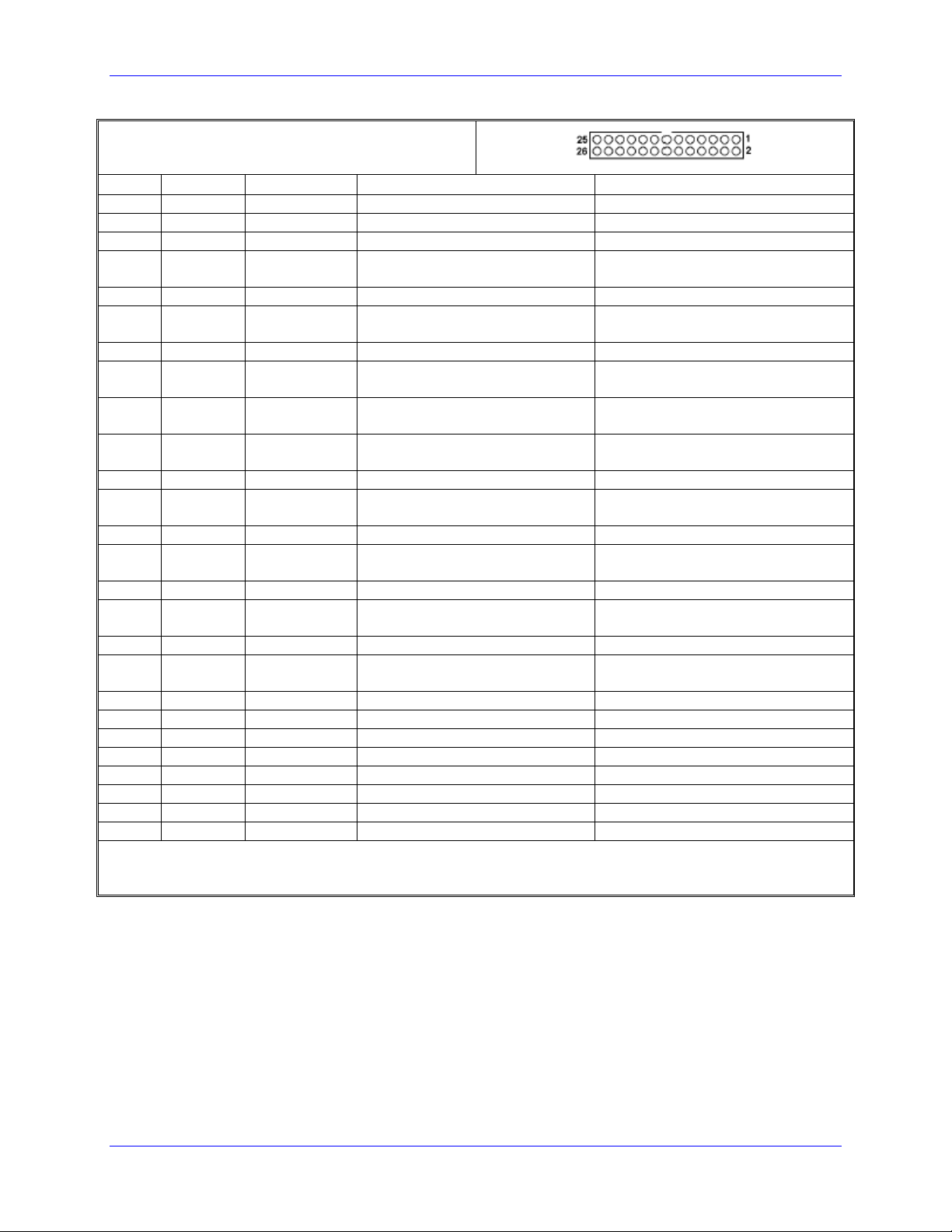
J2/JTHW (26-Pin Header)
Pin # Symbol Function Description Notes
1 GND Common PMAC Common
2 GND Common PMAC Common
3 DAT0 Input Data-0 Input Data input from MUX port accessories
4 SEL0 Output Select-0 Output Address/data output for MUX port
accessories
5 DAT1 Input Data-1 Input Data input from MUX port accessories
6 SEL1 Output Select-1 Output Address/data output for MUX port
accessories
7 DAT2 Input Data-2 Input Data input from MUX port accessories
8 SEL2 Output Select-2 Output Address/data output for MUX port
accessories
9 DAT3 Input Data-3 Input Data Input From MUX Port
Accessories
10 SEL3 Output Select-3 Output Address/data output for MUX port
accessories
11 DAT4 Input Data-4 Input Data input from MUX port accessories
12 SEL4 Output Select-4 Output Address/data output for MUX port
accessories
13 DAT5 Input Data-5 Input Data input from MUX port accessories
14 SEL5 Output Select-5 Output Address/data output for MUX port
accessories
15 DAT6 Input Data-6 Input Data input from MUX port accessories
16 SEL6 Output Select-6 Output Address/data output for MUX port
accessories
17 DAT7 Input Data-7 Input Data input from MUX port accessories
18 SEL7 Output Select-7 Output Address/data output for MUX port
accessories
19 N.C. N.C. No Connection
20 GND Common PMAC Common
21 BRLD/ Output Buffer Request Low is Buffer Req.
22 GND Common PMAC Common
23 IPLD/ Output In Position Low is in position
24 GND Common PMAC Common
25 +5V Output +5Vdc Supply Power supply out
26 INIT/ Input PMAC Reset Low is reset
Note: The JTHW connector provides eight inputs and eight outputs at TTL levels; typically, these are used to create
multiplexed I/O with accessory boards such as Acc-18 (Thumbwheel) and Acc-34 (Discrete I/O). The port I/O may
also be used directly, as non-multiplexed I/O.

PMAC -VME Ultralite Hardware Reference Manual
Connectors and Jumpers
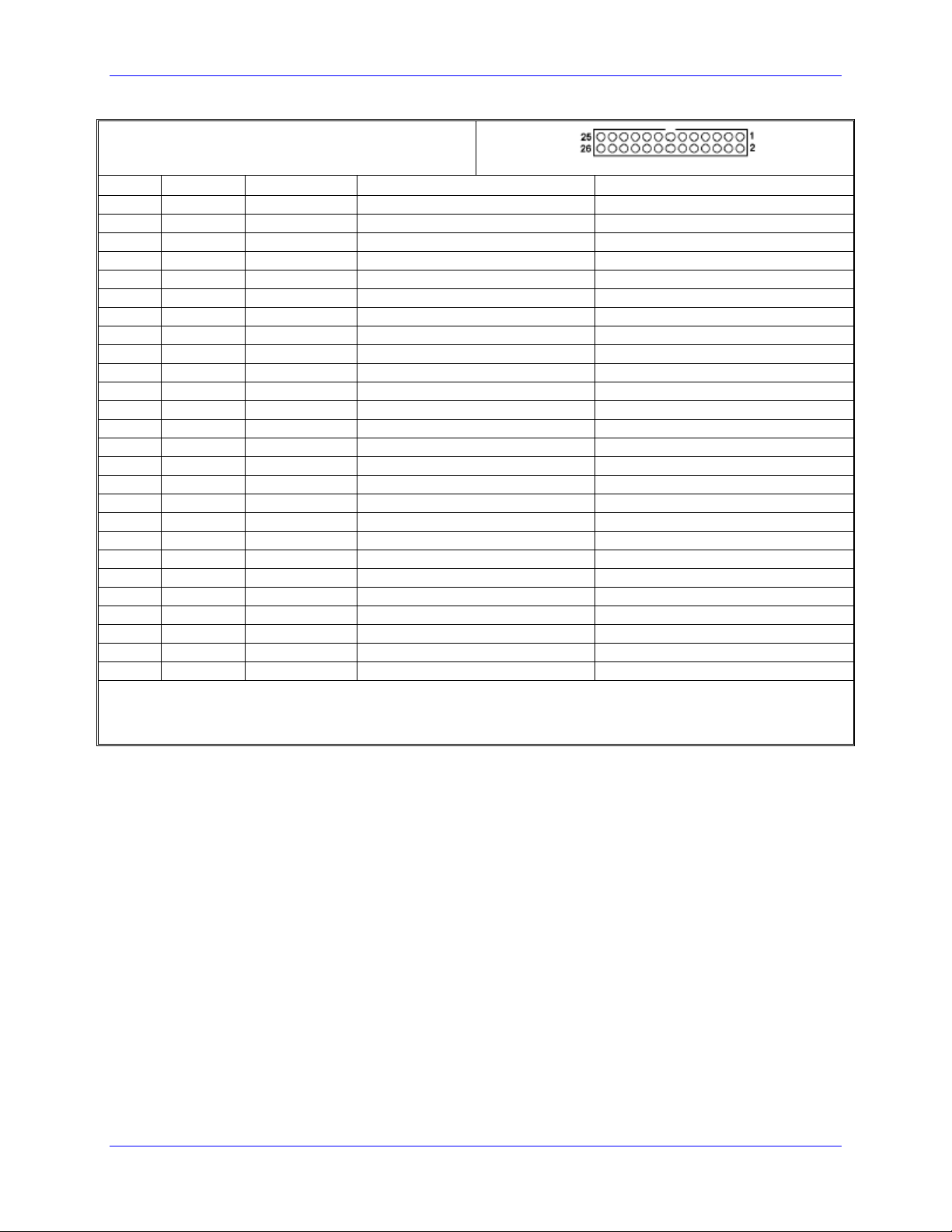
J3/JIO (40-Pin Header)
Pin # Symbol Function Description Notes
1 I/O00 In/Out Digital I/O0 Software direction control
2 I/O01 In/Out Digital I/O 1 Software direction control
3 I/O02 In/Out Digital I/O 2 Software direction control
4 I/O03 In/Out Digital I/O 3 Software direction control
5 I/O04 In/Out Digital I/O 4 Software direction control
6 I/O05 In/Out Digital I/O 5 Software direction control
7 I/O06 In/Out Digital I/O 6 Software direction control
8 I/O07 In/Out Digital I/O 7 Software direction control
9 I/O08 In/Out Digital I/O 8 Software direction control
10 I/O09 In/Out Digital I/O 9 Software direction control
11 I/O10 In/Out Digital I/O 10 Software direction control
12 I/O11 In/Out Digital I/O 11 Software direction control
13 I/O12 In/Out Digital I/O 12 Software direction control
14 I/O24 In/Out Digital I/O 13 Software direction control
15 I/O14 In/Out Digital I/O 14 Software direction control
16 I/O15 In/Out Digital I/O 15 Software direction control
17 I/O16 In/Out Digital I/O 16 Software direction control
18 I/O17 In/Out Digital I/O 17 Software direction control
19 I/O18 In/Out Digital I/O 18 Software direction control
20 I/O29 In/Out Digital I/O 19 Software direction control
21 I/O20 In/Out Digital I/O 20 Software direction control
22 I/O21 In/Out Digital I/O 21 Software direction control
23 I/O22 In/Out Digital I/O 22 Software direction control
24 I/O23 In/Out Digital I/O 23 Software direction control
25 I/O24 In/Out Digital I/O 24 Software direction control
1 I/O00 In/Out Digital I/O 0 Software direction control
26 I/O25 In/Out Digital I/O 25 Software direction control
27 I/O26 In/Out Digital I/O 26 Software direction control
28 I/O27 In/Out Digital I/O 27 Software direction control
29 I/O28 In/Out Digital I/O 28 Software direction control
30 I/O29 In/Out Digital I/O 29 Software direction control
31 I/O30 In/Out Digital I/O 30 Software direction control
32 I/O31 In/out Digital I/O 31 Software direction control
33 GND Common Reference Voltage
34 GND Common Reference Voltage
35 Phase/ Output Phase Clock For latching data
36 Servo/ Output Servo Clock For latching data
37 GND Common Reference Voltage
38 GND Common Reference Voltage
39 +5V Output Supply voltage To power external circuitry
40 +5V Output Supply voltage To power external circuitry
Note: The JI/O connector provides 32 input/output pins at TTL levels. Direction can be controlled in byte-wide
groups.

PMAC2 VME Ultralite Hardware Reference Manual
6 Connectors and Jumpers
J5/JRS232 (10-Pin Header)
Front View
Pin # Symbol Function Description Notes
1 PHASE In/Out Phasing Clock
2 DTR Bidirect Data Term Ready Tied to "DSR"
3 TXD/ Input Receive Data Host transmit data
4 CTS Input Clear to Send Host ready bit
5 RXD/ Output Send Data Host receive data
6 RTS Output Req. to Send PMAC ready bit
7 DSR Bidirect Data Set Ready Tied to "DTR"
8 SERVO In/Out Servo Clock See Note 2
9 GND Common PMAC Common
10 +5V Output +5Vdc Supply Power supply out
The JRS232 connector provides the PMAC2 VME Ultralite with the ability to communicate serially with an RS232
port. Jumpers E17 and E18 must connect pins 1 and 2 to use this port for serial communications.
This connector cannot be used for daisy chain communication interconnection of multiple PMACs, although it can be
used to share servo and phase clocks for synchronicity. The J5A RS-422 interface is required for daisy chain
communication.
Note: If communicating over this connector with a modem-style terminal emulator such as Microsoft Windows
Terminal, line 1 should not be connected. Servo and Phase are outputs if jumper E1 is OFF; they are inputs if jumper
E1 is ON.
PMAC -VME Ultralite Hardware Reference Manual
Connectors and Jumpers
J5A/JRS422 (26-Pin Header)
Front View
Pin # Symbol Function Description Notes
1 CHASSI Common PMAC Common
2 S+5V Output +5Vdc Supply Deactivated by "E8"
3 RD- Input Receive Data Diff. I/O low true **
4 RD+ Input Receive Data Diff. I/O high true*
5 SD- Output Send Data Diff. I/O low true **
6 SD+ Output Send Data Diff. I/O high true *
7 CS+ Input Clear to Send Diff. I/O high true **
8 CS- Input Clear to Send Diff. I/O low true *
9 RS+ Output Req. to Send Diff. I/O high true **
10 RS- Output Req. to Send Diff. I/O low true *
11 DTR Bidirect Data Term Read Tied to "DSR"
12 INIT/ Input PMAC Reset Low is "reset"
13 GND Common PMAC Common **
14 DSR Bidirect Data Set Ready Tied to "DTR"
15 SDIO- Bidirect Special Data Diff I/O low true
16 SDIO+ Bidirect Special Data Diff. I/O high true
17 SCIO- Bidirect Special Ctrl. Diff. I/O low true
18 SCIO+ Bidirect Special Ctrl. Diff. I/O high true
19 SCK- Bidirect Special Clock Diff. I/O low true
20 SCK+ Bidirect Special Clock Diff. I/O high true
21 SERVO- Bidirect Servo Clock Diff. I/O low true***
22 SERVO+ Bidirect Servo Clock Diff. I/O high true ***
23 PHASE Bidirect Phase Clock Diff. I/O low true***
24 PHASE+ Bidirect Phase Clock Diff. I/O high true ***
25 GND Common PMAC Common
26 +5V Output +5Vdc Supply Power supply out
The JRS422 connector provides the PMAC with the ability to communicate in both RS422 and RS232. In addition,
this connector is used to daisy chain interconnect multiple PMACs for synchronized operation.
Note: Jumpers E17 and E18 must connect pins 2 and 3 to use this port for serial communications.

PMAC2 VME Ultralite Hardware Reference Manual
8 Connectors and Jumpers
J6/JDISP (14-Pin Header)
Front View
Pin # Symbol Function Description Notes
1 Vdd Output +5V Power Power supply out
2 Vss Common PMAC Common
3 Rs Output Read Strobe TTL signal out
4 Vee Output Contrast Adjust. Vee 0 to +5 Vdc *
5 E Output Display Enable High is enable
6 R/W Output Read or Write TTL signal out
7 DB1 Output Display Data1
8 DB0 Output Display Data0
9 DB3 Output Display Data3
10 DB2 Output Display Data2
11 DB5 Output Display Data5
12 DB4 Output Display Data4
13 DB7 Output Display Data7
14 DB6 Output Display Data6
The JDISP connector is used to drive the 2 line x 24 character (Acc-12), 2 x 40 (Acc-12A) LCD, or the 2 x 40 vacuum
fluorescent (Acc 12C) display unit. The DISPLAY command may be used to send messages and values to the display.
J7/JHW (20-Pin Header)
Front View
Pin # Symbol Function Description Notes
1 GND Common Reference Voltage
2 +5V Output Supply Voltage To power external Circuitry
3 HWA1+ Input HW Positive A Channel Also pulse input
4 HWA1- Input HW Negative A Channel Also pulse input
5 HWB1+ Input HW Positive B Channel Also direction input
6 HWB1- Input HW Negative B Channel. Also direction input
7 HWA2+ Input HW Positive A Channel Also pulse input
8 HWA2- Input HW Negative A Channel Also pulse input
9 HWB2+ Input HW Positive B Channel Also direction input
10 HWB2- Input HW Negative B Channel Also direction input
1 GND Common Reference Voltage
11 DIR1+ Output PFM Positive Dir. Out Also PWM output
12 DIR1- Output PFM Negative Dir. Out Also PWM output
13 PUL1+ Output PFM Positive Pulse Also PWM output
14 PUL1- Output PFM Negative Pulse Also PWM output
15 DIR2+ Output PFM Positive Dir. Out Also PWM output
16 DIR2- Output PFM Negative Dir. Out Also PWM output
17 PUL2+ Output PFM Positive Pulse Also PWM output
18 PUL2- Output PFM Negative Pulse Also PWM output
19 GND Common Reference Voltage
20 +5V Output Supply Voltage To power external Circuitry
This connector provides the interface for two quadrature encoders, typically to be used as handwheel or time base
master encoders.

PMAC -VME Ultralite Hardware Reference Manual
Connectors and Jumpers
P1 JVME (96-Pin Header)
Front View
Pin # Row A Row B Row C
01 D00 BBSY/ D08
02 D01 BCLR/ D09
03 D02 ACFAIL/ D10
04 D03 B0IN/ D11
05 D04 BG0OUT/ D12
06 D05 BG1IN/ D13
07 D06 BG1OUT/ D14
08 D07 BG2IN/ D15
09 GND BG2OUT/ GND
10 SYSCLK BG3IN/ SYSFAIL/
11 GND BG3OUT/ BERR/
12 DS1/ BR0/ SYSRESET/
13 DS0/ BR1/ LWORD/
14 WRITE/ BR2/ AM5
15 GND BR3/ A23
16 DTACK/ AM0 A22
01 D00 BBSY/ D08
17 GND AM1 A21
18 AS/ AM2 A20
19 GND AM3 A19
20 IACK/ GND A18
21 ACKIN/ ISERCLK A17
22 IACKOUT/ SERDAT/ A16
23 AM4 GND A15
24 A07 IRQ7/ A14
25 A06 IRQ6/ A13
26 A05 IRQ5/ A12
27 A0 IRQ4/ A11
28 A03 IRQ3/ A10
29 A02 IRQ2/ A09
30 A01 IRQ1/ A08
31 -12 +5V STDBY +12V
32 +5V +5V +5V
This is the standard VME connector. It is sufficient for 16-bit or 24-bit addressing and for 8-bit or
16-bit data. For 32-bit addressing, the B-row of P2 must be used as well. PMAC does not support
32-bit data transfers over the bus, even with the B-row of P2.
NOTE: If P1 is connected to the VME backplane, PMAC is connected to the +5V supply and GND
automatically. In this case, no other +5V supply should be connected.

PMAC2 VME Ultralite Hardware Reference Manual
10 Connectors and Jumpers
P2 JVME (96-Pin Header)
Front View
Pin # Row A Row B Row C
01 +5V +5V +5V
02 GND GND GND
03 DB6 (Reserved) DB7
04 DB4 VA24 DB5
05 DB2 VA25 DB3
06 DB0 VA26 DB1
07 R/W- VA27 E
08 Vee VA28 RS
09 CTRL2 VA29 CTRL3
10 CTRL0 VA30 CTRL1
11 No Connect VA31 No Connect
01 +5V +5V +5V
12 No Connect GND No Connect
13 No Connect +5V No Connect
14 No Connect VD16* (Not used) No Connect
15 INIT- VD17* (Not used) BRST-
16 PHASE- VD18* (Not used) PHASE+
17 SERVO- VD19* (Not used) SERVO+
18 RS+ VD20* (Not used) RS-
19 CS+ VD21* (Not used) CS-
20 SD- VD22* (Not used) SD+
21 RD- VD23* (Not used) RD+
22 No Connect GND No Connect
23 PUL_2+ VD24* (Not used) PUL_2-
24 DIR_2+ VD25* (Not used) DIR_2-
25 PUL_1+ VD26* (Not used) PUL_1-
26 DIR_1+ VD27* (Not used) DIR_1-
27 HW2_B2+ VD28* (Not used) HW2_B2-
28 HW2_A2+ VD29* (Not used) HW2_A2-
29 HW1_B1+ VD30* (Not used) HW1_B1-
30 HW1_A1+ VD31* (Not used) HW1_A1-
31 GND GND GND
32 +5V +5V +5V
The P2 connector is only used to support 32-bit addressing on the VME bus. The PMAC2 VME
Ultralite does not support 32-bit data transfers on the VME bus.
Note: Versions of the board before the -102 revision had only no connect on the A and C rows.

PMAC -VME Ultralite Hardware Reference Manual
Connectors and Jumpers
TB1 (2-Pin Terminal Block)
Pin # Symbol Function Description Notes
1 GND Common Reference Voltage
2 +5V Input Positive Supply Voltage Supplies all PMAC digital circuits
This terminal block can be used to provide the input for the power supply for the circuits on the PMAC2 board when it
is not in a bus configuration. When the PMAC2 is in a bus configuration, these supplies come through the bus
connector from the bus power supply automatically; in this case, this terminal block should not be used.
TB2 (3-Pin Terminal Block)
Pin # Symbol Function Description Notes
1 WD_NC Output Watchdog relay out Normally closed
2 COM Input Watchdog return +V or 0V
3 WD_ No Output Watchdog relay out Normally open
Note: The normally closed relay contact is open while PMAC2 is operating properly (it has power and the watchdog
timer is not tripped) and closed when the PMAC2 is not operating properly (either it has lost power or the watchdog
timer has tripped).
This terminal block provides the output for PMAC2’s watchdog timer relay, both normally open and normally closed
contacts. The normally open relay contact is closed while PMAC2 is operating properly and open when PMAC2 is
not operating properly.
MACRO Interface Connectors
Version 1: Fiber Optic Transceiver
• Lower port -transmit optical data
• Upper port - receive optical data
Version 2: Coaxial Cable Connectors
• J12 - receive main data
• J13 - receive complementary data
• J15 - transmit complementary data
• J16 - transmit main data
Version 3: RJ-45 Phone Jack Connectors
• J14 - receive data
• J17 - transmit data
PMAC2 VME Ultralite Hardware Reference Manual
12 Connectors and Jumpers
Jumper Summary
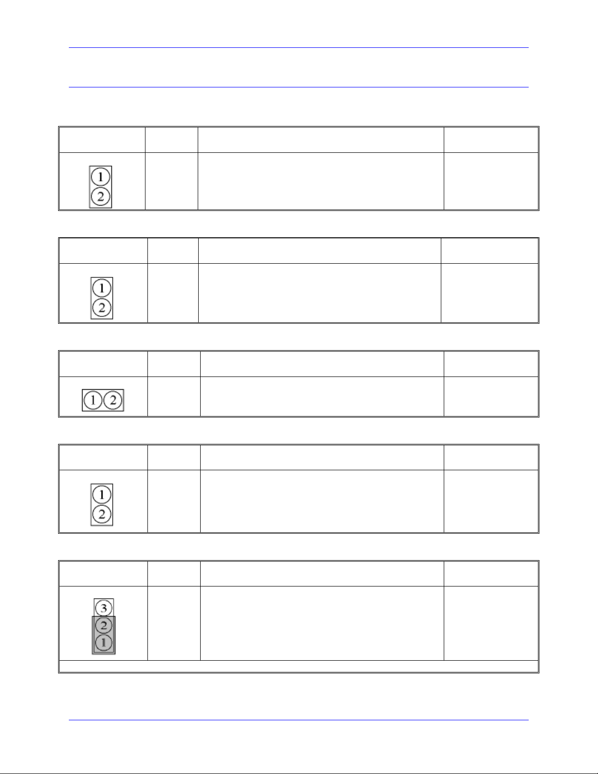
Refer to the PMAC2 VME Ultralite layout diagram (see diagram) for jumper locations.
E1: Card 0 Select
E Point and
Physical Layout Location Description Default
E1
Remove jumper to specify that this PMAC is Card 0, which
generates its own phase and servo clock (default). Jump
pins 1 to 2 to specify that this PMAC is not Card 0, but
Card 1 to F (15), which requires external phase and servo
clock signals from the serial port to operate.
No jumper installed
E2: 40MHz/60MHz CPU Operation
E Point and
Physical Layout Location Description Default
E2
Remove jumper to specify 40 MHz operation of the
PMAC CPU (2 x crystal frequency). Jump pins 1 to 2 to
specify 60 MHz operation of the PMAC CPU (3 x crystal
frequency).
No jumper installed
(standard)
1-2 jumper installed
(Option 5B)
E3: Re-Initialization On Reset Control
E Point and
Physical Layout Location Description Default
E3
Remove jumper for normal reset mode (default). Jump
pins 1 to 2 for re-initialization on reset. No jumper installed
E4-E6: (Reserved For Future Use)
E Point and
Physical Layout Location Description Default
E4-E6
No jumper installed
E7: Multi-Board Daisy-Chain Configure
E Point and
Physical Layout Location Description Default
E7
Jump pin 1 to 2 to receive clock signals over RS-232 port
(single-ended) as board @1 to @F.
Jump pin 2 to 3 to receive clock signals over RS-422 port
(differential) as board @1 to @F.
1-2 Jumper installed
This jumper is only present on prototype PMAC2 VME Ultralite boards (-100).

PMAC -VME Ultralite Hardware Reference Manual
Connectors and Jumpers
E8: RS232 Converter Power Supply Control
E Point and
Physical Layout Location Description Default
E8
Jump pin 1 to 2 to apply +5V to J5A pin 2 (JRS422). This
can be used to power optional RS422 to RS232 converter
module which requires +5V for operation.
Remove jumper to leave pin open.
Jumper installed
Note: This jumper is present only on prototype PMAC2 VME Ultralite boards (-100).
E9 - E16: Serial Interface Handshake Control
E Point and
Physical Layout Location Description Default
E9 E10
Jump E9-1 to E9-2 to allow TXD/ to be input on J5A-11;
jump E10-1 to E10-2 to allow RXD/ to be output on J5A-
13.
Jump E9-1 to E10-1 to allow TXD/ to be output on J5A-11;
jump E9-2 to E10-2 to allow RXD/ to be input on J5A-13.
1-2 Jumpers installed
E11 E12
Jump, E11-1 to E11-2 to allow TXD to be input on J5A-12;
jump E11-1 to E11-2 to allow RXD to be output on J5A-14.
Jump E11-1 to E12-1 to allow TXD to be output on J5A-12;
jump E9-2 to E10-2 to allow RXD to be input on J5A-14.
1-2 Jumpers installed
E13 E14
Jump E13-1 to E13-2 to 1-2 allow RTS to be input on J5A-
15; jump E14-1 to installed E14-2 to allow CTS to be
output on J5A-17.
Jump E13-1 to E14-1 to allow RTS to be output on J5A-15;
jump E13-2 to E14-2 to allow CTS to be input on J5A-17
1-2 Jumpers installed
E15 E16
Jump E15-1 to E15-2 to 1-2 allow RTS/ to be input on J5A-
16; jump E16-1 to E16-2 to allow CTS/ to be output on
J5A-18.
Jump E15-1 to E16-1 to allow RTS/ to be output on J5A-
16; jump E15-2 to E16-2 to allow CTS/ to be input on J5A-
18
1-2 Jumpers installed
Note: E9 -E16 jumpers control whether the RS-422 port is DCE or DTE. They are present only on the prototype
PMAC2 VME Ultralite. The default configuration sets up a DTE device for direction connection to the DCE COM port
of an IBM PC or compatible.

PMAC2 VME Ultralite Hardware Reference Manual
14 Connectors and Jumpers
E15A-H, E16A-H: DPRAM Byte Order Control
E Point and
Physical Layout Location Description Default
E15A-H
Jump pins 1 to 2 to tie DPRAM data lines 8-15 to VMEbus
data lines 8-15 (Motorola big endian format).
Jump pins 2 to 3 to tie DPRAM data lines 8-15 to VMEbus
data lines 0-7 (Intel little endian format)
1-2 Jumpers installed
E16A-H
Jump pins 1 to 2 to tie DPRAM data lines 0-7 to VMEbus
data lines 0-7 (Motorola big endian format).
Jump pins 2 to 3 to tie DPRAM data lines 0-7 to VMEbus
data lines 8-15 (Intel little endian format)
1-2 Jumpers installed
(Motorola format)
Note: This jumper function is implemented differently on the prototype PMAC2 VME Ultralite boards (-100) than it is
on subsequent versions (-101 and greater). All E15A-H and E16A-H jumpers must be in the same setting for
DPRAM communications to work.
E17 - E18: Serial Connector Select
E Point and
Physical Layout Location Description Default
E17
Jump pins 1 to 2 to use RS-232 serial interface.
Jump pins 2 to 3 to use RS-422 serial interface. 1-2 Jumper installed
E18
Jump pins 1 to 2 to use RS-232 serial interface.
Jump pins 2 to 3 to use RS-422 serial interface 1-2 Jumper installed
Note: E17 and E18 control whether the RS-232 or RS-422 serial port is used.
E19: Watchdog Control Jumper
E Point and
Physical Layout Location Description Default
E19
Jump pin 1 to 2 to disable Watchdog timer.
Remove jumper to enable Watchdog timer. No jumper installed
E20-E21: DPRAM Byte Read/Write Order Control
E Point and
Physical Layout Location Description Default
E20 E21
Jump E20-1 to E20-2 to tie VME bus signal VDS0- to
upper byte select of DPRAM; jump E21-1 to E21-2 to tie
VDS1- to lower byte select (Motorola format).
Jump E20-1 to E21-1 to tie VME bus signal VDS0- to
lower byte select of DPRAM; jump E20-2 to E21-2 to tie
VDS1- to upper byte select (Intel Format).
-2 Jumpers installed
Note: This jumper function is implemented differently on the prototype PMAC2 VME Ultralite boards (-100) than it is
on subsequent versions (-101 and greater).

PMAC2 VMEUltralite Hardware Reference Manual
Connectors and Jumpers 15
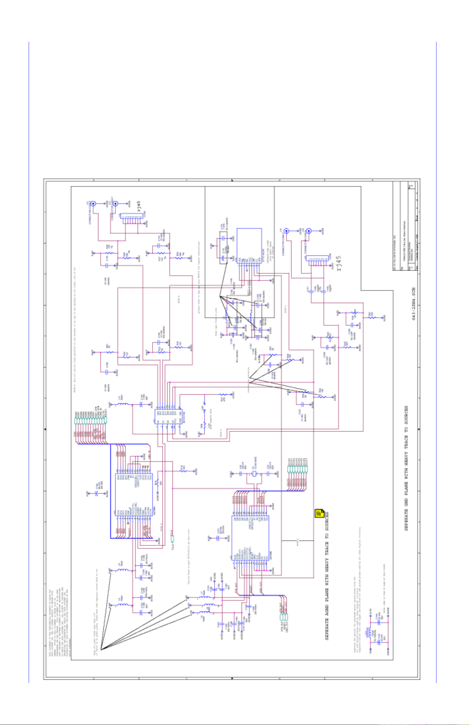
SCHEMATICS
PMAC2 VMEUltralite Hardware Reference Manual
16 Connectors and Jumpers
Other manuals for PMAC2 VME Ultralite
1
Table of contents
Popular Motherboard manuals by other brands


Intersil
Intersil ISL8272MEVAL1Z user guide

Texas Instruments
Texas Instruments OMAP35 Series Migration guide

Lattice Semiconductor
Lattice Semiconductor iCE40 Ultra user guide

Gigabyte
Gigabyte GA-A320M-DS2 user manual

Texas Instruments
Texas Instruments TPA741 MSOP user guide

MATSONIC
MATSONIC MS6380SG user manual