Diamond Systems Jupiter-MM-5000 User manual

JMM-5000 User Manual Rev B.00 www.diamondsystems.com Page 1
Jupiter-MM-5000
Advanced Technology 218W DC/DC Power Supply PC/104-Plus Module
User Manual
Revision B.01
Copyright 2016-2022
FOR TECHNICAL SUPPORT Diamond Systems Corporation
PLEASE CONTACT: 158 Commercial Street
Sunnyvale, CA 94086 USA
[email protected]m Tel 1-650-810-2500
www.diamondsystems.com
Revision
Date
Comment
A.00
1/5/2016
Initial Release
B.00
3/24/16
Updated with Intelligent Model information
B.01
3/22/2022
Added new JMM-5012 models

JMM-5000 User Manual Rev B.01 www.diamondsystems.com Page 2
Contents
1. Important Safe Handling Information........................................................................................................... 3
2. Introduction..................................................................................................................................................... 4
2.1 Key Features........................................................................................................................................ 4
2.2 Cooling ................................................................................................................................................. 5
2.3 LED Indicators...................................................................................................................................... 5
2.1 Available Models .................................................................................................................................. 5
3. Functional Overview...................................................................................................................................... 6
3.1 Functional Block Diagram ........................................................................................................................ 6
3.2 Mechanical Board Drawing ...................................................................................................................... 7
4. Power Supply Operation................................................................................................................................ 9
4.1 Source Selection ...................................................................................................................................... 9
4.2 +5V Output Functionality.......................................................................................................................... 9
4.3 +12V Output Functionality........................................................................................................................ 9
4.4 +3.3V Output Functionality....................................................................................................................... 9
4.5 +5V Standby Output Functionality............................................................................................................ 9
4.6 +3.3V Standby Output Functionality......................................................................................................... 9
4.7 Input Protection ........................................................................................................................................ 9
4.8 Remote On/Off ....................................................................................................................................... 10
4.9 Advanced System Controller.................................................................................................................. 10
5. Connector Location and Description......................................................................................................... 11
6. Connector Pinout and Pin Description...................................................................................................... 12
6.1 Primary Power Input Connector (J7)...................................................................................................... 12
6.2 Secondary Power Input Connector (J8)................................................................................................. 12
6.3 Output Power Connectors (J9 & J10)..................................................................................................... 13
6.4 Remote On/Off Control (J6) ................................................................................................................... 13
6.5 USB Connector for Control Panel Interface (J12).................................................................................. 14
6.6ISA Connectors (J1 & J2)....................................................................................................................... 14
6.7 PC-104 Connector (J3) .......................................................................................................................... 15
7. Installation..................................................................................................................................................... 16
8. Output Voltages and Currents.................................................................................................................... 16
9. Control Software .......................................................................................................................................... 17
10. Specifications............................................................................................................................................... 18

JMM-5000 User Manual Rev B.01 www.diamondsystems.com Page 3
1. IMPORTANT SAFE HANDLING INFORMATION
WARNING!
ESD-Sensitive Electronic Equipment
Observe ESD-safe handling procedures when working with this product.
Always use this product in a properly grounded work area and wear
appropriate ESD-preventive clothing and/or accessories.
Always store this product in ESD-protective packaging when not in use.
Safe Handling Precautions
The board contains a high density connector with many connections to sensitive electronic components. This
creates many opportunities for accidental damage during handling, installation and connection to other equipment.
The list here describes common causes of failure found on boards returned to Diamond Systems for repair. This
information is provided as asource of advice to help youprevent damaging your Diamond (or any vendor’s) boards.
ESD damage –This type of damage is usually almost impossible to detect, because there is no visual sign of
failure or damage. The symptom is that the board eventually simply stops working, because some component
becomes defective. Usually the failure can be identified and the chip can be replaced. To prevent ESD damage,
always follow proper ESD-prevention practices when handling computer boards.
Damage during handling or storage –On some boards we have noticed physical damage from mishandling. A
common observation is that a screwdriver slipped while installing the board, causing a gouge in the PCB surface
and cutting signal traces or damaging components.
Another common observation is damaged board corners, indicating the board was dropped. This may or may not
cause damage to the circuitry, depending on what is near the corner. Most of our boards are designed with at least
25 mils clearance between the board edge and any component pad, and ground / power planes are at least 20
mils from the edge to avoid possible shorting from this type of damage. However these design rules are not
sufficient to prevent damage in all situations.
A third cause of failure is when a metal screwdriver tip slips, or a screw drops onto the board while it is powered
on, causing a short between a power pin and a signal pin on a component. This can cause overvoltage / power
supply problems described below. To avoid this type of failure, only perform assembly operations when the system
is powered off.
Sometimes boards are stored in racks with slots that grip the edge of the board. This is a common practice for
board manufacturers. However our boards are generally very dense, and if the board has components very close
to the board edge, they can be damaged or even knocked off the board when the board tilts back in the rack.
Diamond recommends that all our boards be stored only in individual ESD-safe packaging. If multiple boards are
stored together, they should be contained in bins with dividers between boards. Do not pile boards on top of each
other or cram too many boards into a small location. This can cause damage to connector pins or fragile
components.
Power supply wired backwards –Our power supplies and boards are not designed to withstand a reverse power
supply connection. This will destroy each IC that is connected to the power supply (i.e. almost all ICs). In this case
the board will most likely will be unrepairable and must be replaced. A chip destroyed by reverse power or by
excessive power will often have a visible hole on the top or show some deformation on the top surface due to
vaporization inside the package. Check twice before applying power!
Overvoltage on analog input –If a voltage applied to an analog input exceeds the design specification of the
board, the input multiplexor and/or parts behind it can be damaged. Most of our boards will withstand an erroneous
connection of up to 36V on the analog inputs, even when the board is powered off, but not all boards, and not in
all conditions.
Overvoltage on analog output –If an analog output is accidentally connected to another output signal or a power
supply voltage, the output can be damaged. On most of our boards, a short circuit to ground on an analog output
will not cause trouble.
Overvoltage on digital I/O line –If a Digital I/O is connected to a voltage above the maximum specified voltage,
the digital circuitry can be damaged. On most of our boards the acceptable range of voltages connected to digital
I/O signals is 0-5V, and they can withstand about 0.5V beyond that (-0.5 to 5.5V) before being damaged. However
logic signals at 12V and even 24V are common, and if one of these is connected to a 5V logic chip, the chip will
be damaged, and the damage could even extend past that chip to others in the circuit.
JMM-5000 User Manual Rev B.01 www.diamondsystems.com Page 4
2. INTRODUCTION
Jupiter-MM-5000 is a family of PC/104-Plus and PC/104 DC/DC power supplies with wide input range and high
output power. The nominal output power is 5VDC @ 100 Watts at 25oC (5VDC @ 20A), with additional power
provided on 12V and +3.3V rails plus +5V and +3.3V standbyvoltages optional. The output power may be de-rated
at the high end of the temperature range based on the cooling capacity of the thermal solution, as well as de-rated
at low input voltages based on the current capacity of the input circuit and connector.
Available in both basic and intelligent models, the intelligent models offer complete software programmability of
the power supply.
2.1 Key Features
Up to 218W total output power at 25oC
+5VDC at 20A maximum output (100W)
+12VDC at 8A maximum output (96W)
+3.3VDC at 5A maximum output (16.5W)
+5VDC standby option at 1A maximum output (5W)
+3.3VDC standby option at 0.1A maximum output (0.33W)
Extreme load stability: 0.35% maximum output voltage droop at 5V output, 0-20A load, VIN = 12V, TA=
25ºC
Extremely low ripple: 12mV peak-to-peak ripple at 5V output, 0-20A load, VIN = 12V, TA= 25ºC
High efficiency: 92-94% at 5V output, 0-20A load, VIN = 12V, TA= 25ºC
Excellent transient load response: +/-72mV at 5V output, 25-75% load step, 2.5A/usec ramp rate, VIN =
24V, TA= 25ºC
Extreme temperature stability: +/-0.5% at 5V output, 10A load, VIN = 24V, TA= -40ºC to +85ºC
Input protection circuit protects from over/under voltage, reverse polarity, surges, transients, reflected
noise
Advanced System Controller with:
oIndividual supply on/off control for all voltage outputs
oIndividual supply output voltage / current monitoring
oOutput voltage sequencing and slew rate control
oOutput voltage monitoring
oFault handling based on programmable limits with interrupt notification, including supply shutdown
in case of overload or other programmed conditions
oHiccup mode for auto-restart when fault conditions are removed
oMin / max voltage and temperature logging
oSecondary input cutover voltage selection
Wide input range: +7 to +34VDC
Heat sink or heat spreader cooling solutions
PC/104 form factor: 3.550” x 3.775” (90mm x 96mm)
PC/104 and PC/104-Plus bus connector options
-40oC to +85oC (-40°F to +185°F) operating temperature
MIL-STD-202G shock and vibration compatible
.

JMM-5000 User Manual Rev B.01 www.diamondsystems.com Page 5
2.2 Cooling
All significant heat generating components are mounted on the top side of the board and are thermally connected
to the thermal solution with thermal pads. The JMM-5000 power supply offers two cooling methods:
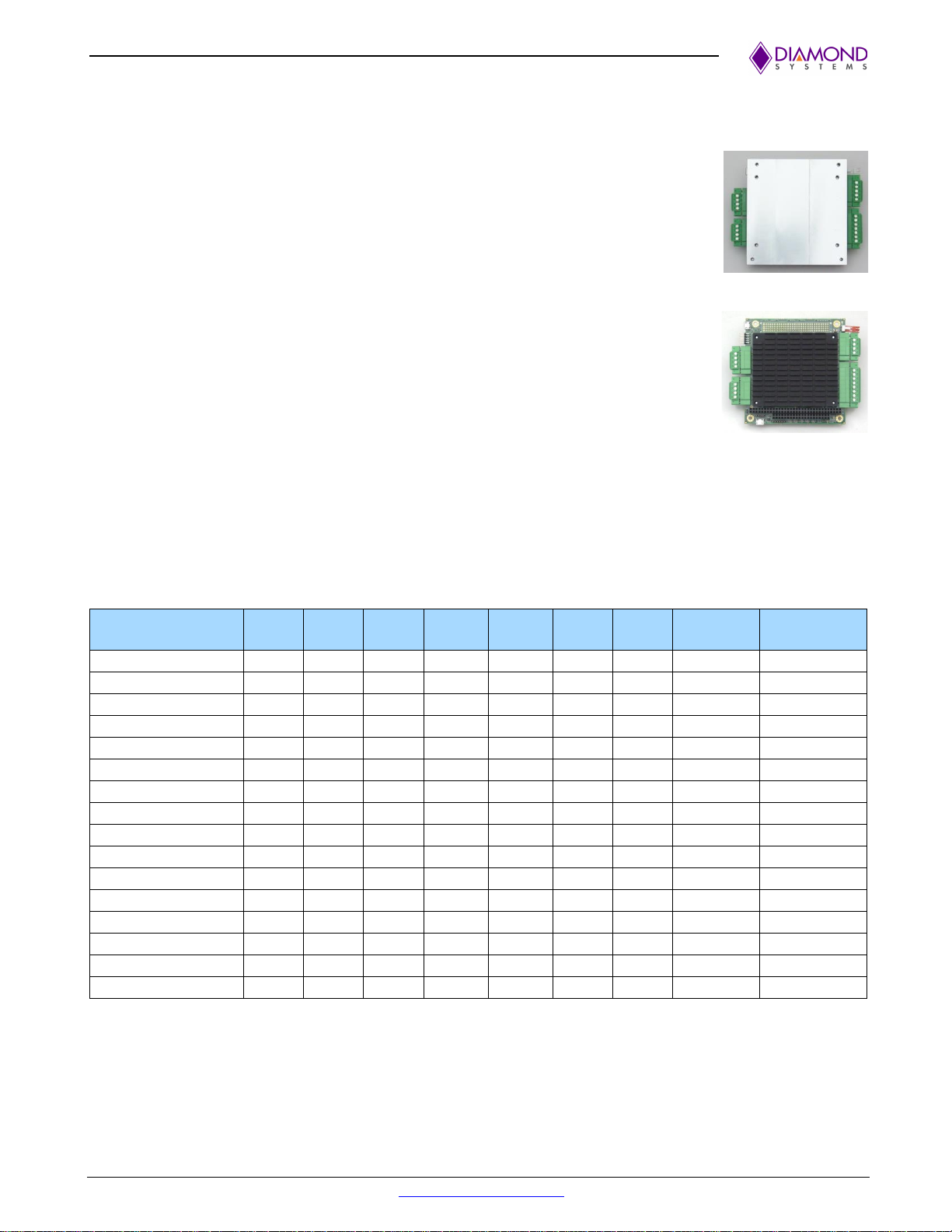
Heat spreader: A heat spreader on the top side may be used for all cooling as shown at
the right. The heat spreader is the size and shape of the PC/104 board. It contains the
standard mounting hole patterns for #6 and M3 screws. The Diamond Systems’ PC/104
heat sink accessory may be installed on top of this heat spreader as an option. When the
heat spreader is installed, the PC/104 and PC/104-Plus connectors have bottom-side pins
only and do not support stacking of modules on the top side of the board. The heat spreader
configuration, when attached to a suitable heat dissipation surface or when the heat sink
accessory is installed, supports the full power output at 85oC. The heat spreader supports the installation of PC/104
heat sink accessory ACC-HS104-12.7.
Heat sink: A low profile heat sink may be installed on the board in the area between the
PC/104 and PC/104-Plus connectors as shown at the right. The heat sink should be used
only in applications with power dissipation of 100W or less. The height of the heat sink
conforms to PC/104 height limits of 0.435” / 11mm max height above the PCB top surface.
The heat sink configuration may have a lower total output power capacity at 85oC and/or a
lower maximum operating temperature at full power output.
2.3 LED Indicators
A green LED is provided for each output voltage to indicate proper operation. The LEDs are located along the
lower edge of the PCB below thePC/104 connector. All LEDs are calibrated tohave equal brightness at the nominal
output voltage for their designated power supply.
2.1 Available Models
Model
5V
20A
12V
8A
3.3V
5A
5V
Standby
3.3V
Standby
ISA
Bus
PCI
Bus
System
Controller
Thermal
JMM-5312-APDRH
Yes
Yes
Yes
Yes
Yes
Yes
Yes
Yes
Heat spreader
JMM-5312-APDRK
Yes
Yes
Yes
Yes
Yes
Yes
Yes
Yes
Heat sink
JMM-5312-ADRH
Yes
Yes
Yes
Yes
Yes
Yes
Yes
Heat spreader
JMM-5312-ADRK
Yes
Yes
Yes
Yes
Yes
Yes
Yes
Heat sink
JMM-5012-APDRH
Yes
Yes
Yes
Yes
Yes
Yes
Heat spreader
JMM-5012-APDRK
Yes
Yes
Yes
Yes
Yes
Yes
Heat sink
JMM-5012-ADRH
Yes
Yes
Yes
Yes
Yes
Heat spreader
JMM-5012-ADRK
Yes
Yes
Yes
Yes
Yes
Heat sink
JMM-5012-APH
Yes
Yes
Yes
Yes
Yes
Heat spreader
JMM-5012-APK
Yes
Yes
Yes
Yes
Yes
Heat sink
JMM-5012-AH
Yes
Yes
Yes
Yes
Heat spreader
JMM-5012-AK
Yes
Yes
Yes
Yes
Heat sink
JMM-5000-APH
Yes
Yes
Yes
Heat spreader
JMM-5000-APK
Yes
Yes
Yes
Heat sink
JMM-5000-AH
Yes
Yes
Heat spreader
JMM-5000-AK
Yes
Yes
Heat sink

JMM-5000 User Manual Rev B.01 www.diamondsystems.com Page 6
3. FUNCTIONAL OVERVIEW
3.1 Functional Block Diagram
Figure 1 shows the block diagram for the Jupiter-MM-5000 family. All models of the family are represented in the
lock diagram with the items in green only being included on the full featured intelligent models.
Figure 1: Block Diagram

JMM-5000 User Manual Rev B.00 www.diamondsystems.com Page 7
3.2 Mechanical Board Drawing
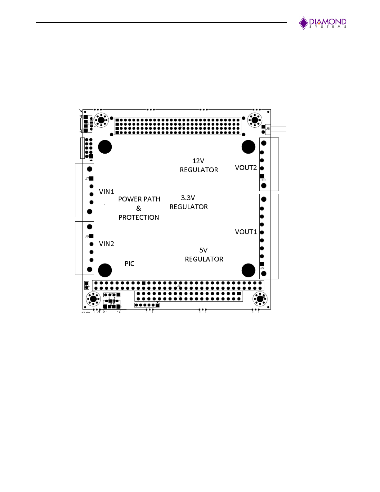
Figure 2 shows the mechanical drawing for Jupiter-MM-5000 with locations of the key features. Figure 3 is a
dimensioned drawing of the Jupiter-MM-5000. The power supply modules adhere to the PC/104-Plus standard.

JMM-5000 User Manual Rev B.01 www.diamondsystems.com Page 9
4. POWER SUPPLY OPERATION
4.1 Source Selection
The power supply takes its input from either the main input connector or the optional backup / battery input
connector, with precedence given to the main input connector. If the input voltage on the main input connector is
above the designated threshold voltage, it will be used as the source for the power supply. If the input voltage falls
below the minimum, the supply will automatically switch to the backup / battery input. If this secondary input does
not have sufficient voltage, the supply will shut off.
The design supports the use of either single or dual power sources using the LTC4417 chip.
4.2 +5V Output Functionality
The +5V output uses a multi-phase design. The 5V is generated from a dual LTC3890 switch. Each switch output
can produce up to 5A of output current for a total of 20A capacity with all 4 outputs enabled. In this fashion the
output efficiency can be optimized based on the load, resulting in higher efficiency across the full rated output
power of the supply.
4.3 +12V Output Functionality
The LT3790 synchronous 4-switch buck-boost voltage/ current regulator controller is used for generating +12V
output. The current output is limited to 8A maximum.
4.4 +3.3V Output Functionality
A TI-based power module is used for generating +3.3V output at 5A maximum. The LMZ31710 is a SIMPLE
SWITCHER power module and an easy-to-use integrated power solution that combines a 10A DC/DC converter
with power MOSFETs, a shielded inductor, and passives in a low profile, QFN package. The module is powered
using the 5V supply.
4.5 +5V Standby Output Functionality
A LT8620 2A regulator is used for the +5V standby supply. The +5V standby supply is used to supply the power
controller and to generate the +3.3V standby voltage. +5V standby at 1A maximum is available at the output
connector.
4.6 +3.3V Standby Output Functionality
The AP7167-SPG-13 is used for generating the +3.3V standby supply. The +3.3V standby supply is used to supply
the PIC microcontroller and the USB to I2C chip. 3.3V standby 0.1A maximum is available at the output connector.
4.7 Input Protection
JMM-5000 includes an input protection circuit based on the LTC4364 chip. This device provides surge / spike
protection, load dump protection, overvoltage / under voltage protection, reverse polarity protection, and input
current limiting (circuit breaker). Filtering is also added to limit noise reflected back onto the input.

JMM-5000 User Manual Rev B.01 www.diamondsystems.com Page 10
4.8 Remote On/Off
The power supply can be switched on and off remotely in two ways; through a discrete logic input or through a
programmable serial command.
For the discrete logic input, a 2-pin connector is used to provide an on/off control and ground. Driving the on/off
control to a logic 0, or shorting it to the power supply common, will shut off all supply outputs (except the auxiliary
+5V for the microcontroller and power controller circuit). The control input has a pull-up resistor to drive it to a
default on state. The remote on/off circuit is always operational when appropriate power is supplied through either
the main input or the backup / battery input connections.
Usage of the programmable serial command remote on/off can be found in the Janus-MM-5000 Software Users
Manual.
4.9 Advanced System Controller
The intelligent Jupiter-5000 models include a system controller that offers advanced configuration, control, and
monitoring features. The system controller is accessed via a USB port and is accompanied by benchtop
configuration software as well as an application library for in-application real-time control.
•Individual supply on/off control for +12V, +5V, and +3.3V outputs
•Individual supply output voltage / current monitoring
•Output voltage sequencing and slew rate control
•Output voltage adjustment
•Input voltage monitoring
•Fault handling based on programmable limits with interrupt notification, including supply shutdown in case of
overload or other programmed conditions
•Hiccup mode for auto-restart when fault conditions are removed
•Min / max voltage and temperature logging
•Secondary input cutover voltage selection
Information on using the advanced systems controller can be found in theJanus-MM-5000 Software Users Manual.

JMM-5000 User Manual Rev B.01 www.diamondsystems.com Page 11
5. CONNECTOR LOCATION AND DESCRIPTION
(Heat sink removed for clarity)
J1
ISA Bus (PC/104) main connector
J2
ISA Bus (PC/104) 16-bit extension connector
J3
PCI Bus connector (PCI-104)
J4
Not present
J5
Factory use (microcontroller programming)
J6
Not present
J7
Primary input power connector
J8
Secondary input power connector
J9
5V / 5V standby output connector
J10
12V / 3.3V / 3.3V standby output connector
J11
Not present
J12
USB connector to communicate between power management
microcontroller and host PC

JMM-5000 User Manual Rev B.01 www.diamondsystems.com Page 12
6. CONNECTOR PINOUT AND PIN DESCRIPTION
6.1 Primary Power Input Connector (J7)
A four position screw terminal block is used to provide main input power to the board. This terminal block is located
along the left side of the board. The connector supports 16A total on the two input terminals and 16A total on the
two ground terminals.
J7
Vin 7-34VDC
1
Vin 7-34VDC
2
GND
3
GND
4
Connector Part Number: 1827884
Mating Part Number: 1827729
6.2 Secondary Power Input Connector (J8)
Power can also be provided from a battery source through the connector J8. A 4-position screw terminal block is
used to provide backup / battery input power to the board. The minus terminal is connected to the power supply
common. This terminal block is located along the left side of the board. The connector supports 8A on each
terminal.
J8
Vin 7-34VDC
1
Vin 7-34VDC
2
GND
3
GND
4
Connector Part Number: 1827884
Mating Part Number: 1827729

JMM-5000 User Manual Rev B.01 www.diamondsystems.com Page 13
6.3 Output Power Connectors (J9 & J10)
Two screw terminal blocks are used for output power. J9 is a 7-pin block provides +5V and +5V standby output.
J10 is a 5-pin block and provides +12V, +3.3V, and +3.3V standby outputs. Following are the pinouts for the
mentioned connectors.
J9 J10
+5V out
1
+3.3V standby
1
+5V out
2
+12V out
2
+5V out
3
+3.3V out
3
GND
4
GND
4
GND
5
GND
5
GND
6
+5V standby
7
Connector J9:
Part Number: 1827910
Mating part Number: 1827758
Connector J10:
Part Number: 1827897
Mating part Number: 640621-2
6.4 Remote On/Off Control (J6)
A 2-position latching pin header can be used to connect a remote on/off signal to the power supply. This connector
is located along the right side of the board. An active low signal / contact closure between the input and ground
will turn off all outputs.
J6
On/Off
1
GND
2
Part Number: 640457-2
Mating part Number: 1827732

JMM-5000 User Manual Rev B.01 www.diamondsystems.com Page 14
6.5 USB Connector for Control Panel Interface (J12)
A micro USB connector is used for the USB interface to the PIC microcontroller for communication between host
SBC and PIC microcontroller.
1
VBUS
2
D-
3
D+
4
NC
5
Gnd
Part Number: 10118194-0001LF
6.6 ISA Connectors (J1 & J2)
For simplicity, signal names are only shown for pins with connections on board. All remaining pins are not used
on JMM-HP.
J2: PC/104 8-bit bus connector J1: PC/104 16-bit bus connector
A1
B1
Ground
A2
B2
A3
B3
+5V
A4
B4
A5
B5
-5V
A6
B6
A7
B7
-12V
A8
B8
Ground
D0
C0
Ground
A9
B9
+12V
D1
C1
A10
B10
D2
C2
A11
B11
D3
C3
A12
B12
D4
C4
A13
B13
D5
C5
A14
B14
D6
C6
A15
B15
D7
C7
A16
B16
D8
C8
A17
B17
D9
C9
A18
B18
D10
C10
A19
B19
D11
C11
A20
B20
D12
C12
A21
B21
D13
C13
A22
B22
D14
C14
A23
B23
D15
C15
A24
B24
+5V
D16
C16
A25
B25
D17
C17
A26
B26
Ground
D18
C18
A27
B27
Ground
D19
C19
A28
B28
A29
B29
+5V
A30
B30
A31
B31
Ground
Ground
A32
B32
Ground
Connector Part Number / Description
J1: EPT Connectors 962-60323-12 64 pins .435” high solder tails
J2: EPT Connectors 962-60203-12 40 pins .435” high solder tails

JMM-5000 User Manual Rev B.01 www.diamondsystems.com Page 15
6.7 PC-104 Connector (J3)
The board contains a PC-104 connector, J3, on the top side in the standard position as described by the PC/104-
Plus specification.
J3
Pin
A
B
C
D
1
GND/5.0V KEY2
Reserved
+5
AD00
2
VI/O
AD02
AD01
+5V
3
AD05
GND
AD04
AD03
4
C/BE0*
AD07
GND
AD06
5
GND
AD09
AD08
GND
6
AD11
VI/O
AD10
M66EN
7
AD14
AD13
GND
AD12
8
+3.3V
C/BE1*
AD15
+3.3V
9
SERR*
GND
SB0*
PAR
10
GND
PERR*
+3.3V
SDONE
11
STOP*
+3.3V
LOCK*
GND
12
+3.3V
TRDY*
GND
DEVSEL*
13
FRAME*
GND
IRDY*
+3.3V
14
GND
AD16
+3.3V
C/BE2*
15
AD18
+3.3V
AD17
GND
16
AD21
AD20
GND
AD19
17
+3.3V
AD23
AD22
+3.3V
18
IDSEL0
GND
IDSEL1
IDSEL2
19
AD24
C/BE3*
VI/O
IDSEL3
20
GND
AD26
AD25
GND
21
AD29
+5V
AD28
AD27
22
+5V
AD30
GND
AD31
23
REQ0*
GND
REQ1*
VI/O
24
GND
REQ2*
+5V
GNT0*
25
GNT1*
VI/O
GNT2*
GND
26
+5V
CLK0
GND
CLK1
27
CLK2
+5V
CLK3
GND
28
GND
INTD*
+5V
RST*
29
+12V
INTA*
INTB*
INTC*
30
-12V
Reserved
Reserved
GND/3.3V KEY2
Connector Type: 30 x 4 pin 2mm pitch with solder tails

JMM-5000 User Manual Rev B.00 www.diamondsystems.com Page 16
7. INSTALLATION
All JMM-5000 power supplies are load tested prior to shipping. The power supplies ship with all the external
connectors required to start using your power supply immediately.
No user configuration is required for any version of JMM-5000. Simply plug in the input power and the supply is
operational. To power up your supply:
1. For protection, if you are unfamiliar with the use of this product, do not plug any other boards onto it
when powering it up for the first time.
2. Connect a DC source to the primary power input connector, J7, or to the secondary power input
connector, J8, if it is available. The supply will operate with input voltages from +7 to +34VDC.
CAUTION: Voltages above 35V will be shunted to ground through a transient voltage suppressor (TVS)
on the board. The TVS is rated for 1,500 watt surges. However it could be damaged by sustained
voltages above 35V.
3. Once the input voltage is in the valid range, verify that the proper power output indicator LEDs along the
lower edge of the board are illuminated. This verifies your input power connections and the power supply
is fully functional. Note that only indicators corresponding to the voltages available on the supply will be
lit.
4. Power down the supply. Plug the supply into your PC/104 stack. Your system is ready to use.
8. OUTPUT VOLTAGES AND CURRENTS
JMM-5000 provides output voltages based on the model and options ordered. The outputs appear on the PC/104
bus headers J1 / J2 as well as on the output power connectors J9 and J10. The table below lists the maximum
ratings for each output voltage on each base Jupiter-5000 model.
Output
JMM-5000
JMM-5012
JMM-5312
+5V
20A
20A
20A
+12V
-
8A
8A
+3.3V
-
-
5A
+5V standby
-
-
1A
+3.3V standby
-
-
0.1A

JMM-5000 User Manual Rev B.01 www.diamondsystems.com Page 17
9. CONTROL SOFTWARE
JMM-5000 models with the advanced system controller (models with AD in the part number) are accompanied by
two software products:
•Graphical user interface program for Windows for configuration and monitoring
•Programing library for real-time control and monitoring of the power supply in the system software
User manuals for both software packages are available from the support tab on the product web page:
https://www.diamondsystems.com/products/jupiter5000
The graphical user interface (GUI) program provides a control panel that provides access to all the features of the
power supply. An example screenshot is shown below. The GUI is typically used in a factory environment for
configuring the power supply prior to installation in the end system, and it can also be used for testing and
diagnostic purposes.
The programming library includes a driver and a set of functions that can be incorporated into a C language
program to execute all the functions available in the GUI program. The system software can monitor the power
supply performance in real-time for various purposes including health check, prevention of system overload, and
software-driven power cycling.

JMM-5000 User Manual Rev B.01 www.diamondsystems.com Page 18
10. SPECIFICATIONS
Input
Input voltage
7 –34VDC
Input protection
Over / under voltage, reverse polarity, surges, transients, reflected
noise
Output
Output voltage/current
+5V at 20A maximum
+12V at 8A maximum
+3.3V at 5A maximum
+5V standby at 1A maximum
+3.3V standby at 0.1A maximum
Output protection
Current limit and short circuit protection
Load regulation
±0.8%, Vmin to Vmax, 0-100% load on all outputs, -40°C to +85°C
0.35% maximum output voltage droop at 5V output, 0-20A load,
VIN = 12V, TA= 25°C
Output ripple
44mV peak-to-peak maximum
12mV peak-to-peak at 5V output, 0-20A load, VIN = 12V, TA= 25°C
Efficiency
92-94% at5V output, 0-20A load, VIN = 12V, TA= 25°C
Transient load response
+/-72mV at 5V output, 25-75% load step, 2.5A/usec ramp rate,
VIN = 24V, TA= 25°C
Temperature stability
+/-0.5% at 5V output, 10A load, VIN = 24V, TA= -40°C to 85°C
General
On / Off
Remote or programmable on/off logic input
Dimensions
PC/104 form factor:
3.55” x 3.775” (90mm x 96mm) not including screw terminals
Maximum height .435” (11mm) above PCB top surface
Bus connection options
16-bit stackthrough ISA bus
32-bit PCI bus
Operating temperature
-40°C to +85°C (-40°F to +185°F)
Operating humidity
5 to 95% non-condensing
Shock
MIL-STD-202G compatible
Vibration
MIL-STD-202G compatible
Weight
6.3oz (178.6g) heat sink
8.1oz (229.6g) heat spreader
RoHS
Compliant
This manual suits for next models
16
Table of contents
Other Diamond Systems Power Supply manuals