DX Connection QSK 2500 User manual

DxConnection@frontier.com
10/1/15 Page 1 of 11
DX Connection
QSK 2500© Instruction Manual
1) Description
The DX Connection QSK 2500© allows operating a non-QSK a plifier in QSK ode with no a plifier
odifications. No a plifier T/R relay interface is required. The QSK unit will interface to a plifiers
whose key jack presents less than 200 volts positive or negative polarity to the QSK unit. The QSK 2500©
adds a no inal 10 s delay to the transceiver’s nor al RF delay to eli inate hot switching of the
a plifier’s internal T/R changeover relay before the first dit or dah of a trans ission. After the first dit
or dah, the a plifier re ains keyed up for the re ainder of the trans ission preventing excessive T/R
relay switching. The QSK 2500© returns the a plifier to standby 2 sec to 10 sec (user settable) following
the last dit or dah of a trans ission. The QSK unit incorporates hot switching T/R relay protection
caused by so e transceivers re oving the a plifier key signal before the RF envelop has decayed. The
QSK unit senses for RF on the a plifier RF input connector and only switches fro Trans it-to-Receive
when the RF envelop is no longer present. A functional block diagra is included later in this anual.
The QSK 2500© Key/Paddle input jack accepts a straight key, an external keyer, a bug, a paddle (to use
the transceiver’s internal keyer), co puter generated CW, or anything that keys the transceiver by
grounding a circuit(s). The input device ust sink about 1 a to ground and acco odate 5 volts open
circuit. These require ents are co patible with transceiver’s Key/Paddle Input jack require ents.
2) Specifications
a) RF Power: 2500 Watts CW/SSB/Data odes
b) Antenna VSWR: < 1.5:1 at 2.5KW, < 2.5:1 at 1.5KW
c) RF losses: al ost lossless relays ( uch less loss than PIN diodes), silver plated SO-239 connectors
d) QSK internal relays: acoustically quieted and sealed for quiet operation
e) No hot switching of QSK internal relays
f) Provides T/R relay high voltage interface for both new and older a plifiers: The QSK 2500© input
presents a 5VDC 1 a signal to transceiver A p key jack. The QSK 2500© output keys (to ground)

DxConnection@frontier.com
10/1/15 Page 2 of 11
a plifier T/R relays up to +/-200VDC and 100 a. (No need for MFJ ARB-704 or Jackson Harbor
Keyall Interface.)
g) A plifier TX-to-RX hot switching protection: QSK unit returns to Rx ode only after the RF
envelop has decayed preventing hot switching the a plifier T/R relay.
h) A plifier RX-to-TX hot switching protection: QSK unit adds no inally 10 s (see next ite ) of
delay to the transceiver’s internal 5 to 15 s ti e delay (see Table 1 below) before the start of the
transceiver RF envelop output. The 15 to 25 s total ti e delay allows the a plifier T/R
changeover relay a ple ti e to switch to TX prior to the first dit or dah of each trans ission. The
a plifier re ains keyed after the first dit or dah of each trans ission preventing excessive T/R
relay switching during the trans ission.
i) QSK ti ing delay: The Key/Paddle output to the transceiver is delayed 10 s fro Key/Paddle
input with the factory settings. This should acco odate al ost all transceiver/a plifier
co binations. However, solder ju pers are provided to adjust this ti ing delay fro 4 s to
16 s to acco odate custo transceiver/a plifier ti ing require ents.
j) A plifier keying delay following the last dit or dah of a trans ission: User adjustable fro 2 sec
to 10 sec (factory setting: 3sec)
k) Duty cycle: continuous duty
l) DC power input: 17 to 25 volts at 200 a ( ax) [120VAC power block included.]
) Two LED indicators: Power On (green), Trans it (red)
n) Acoustically-quieted, sealed relays for quiet operation
o) Key/Paddle input jack: 1/4” stereo
p) Xcr Key/Paddle output jack: 1/8” ini stereo
q) A p Key ‘IN’ phono jack: 5VDC open; 1 a (transceiver keys to ground)
r) A p Key ‘OUT’ phono jack: keys A p T/R relay to ground. Accepts T/R relay voltages +2 to +200
VDC or -2 to -200 VDC, 100 a ( ax)
s) Power jack: 2.1 ale (center positive)
t) Size: 5 ¼ in W x 2 in H x 3 in D (excluding SO-239 connectors)
u) Weight: < 1 lb.
v) Optional cables: Standard ini-stereo and RCA cables are available in 3 or 6 foot lengths.
Specify cable type for availability and price.
w) Factory option to use the Kenwood transceiver +12VDC A p Key output signal: Contact DX
Connection for infor ation.
(back view)

DxConnection@frontier.com
10/1/15 Page 3 of 11
3) Interconnections
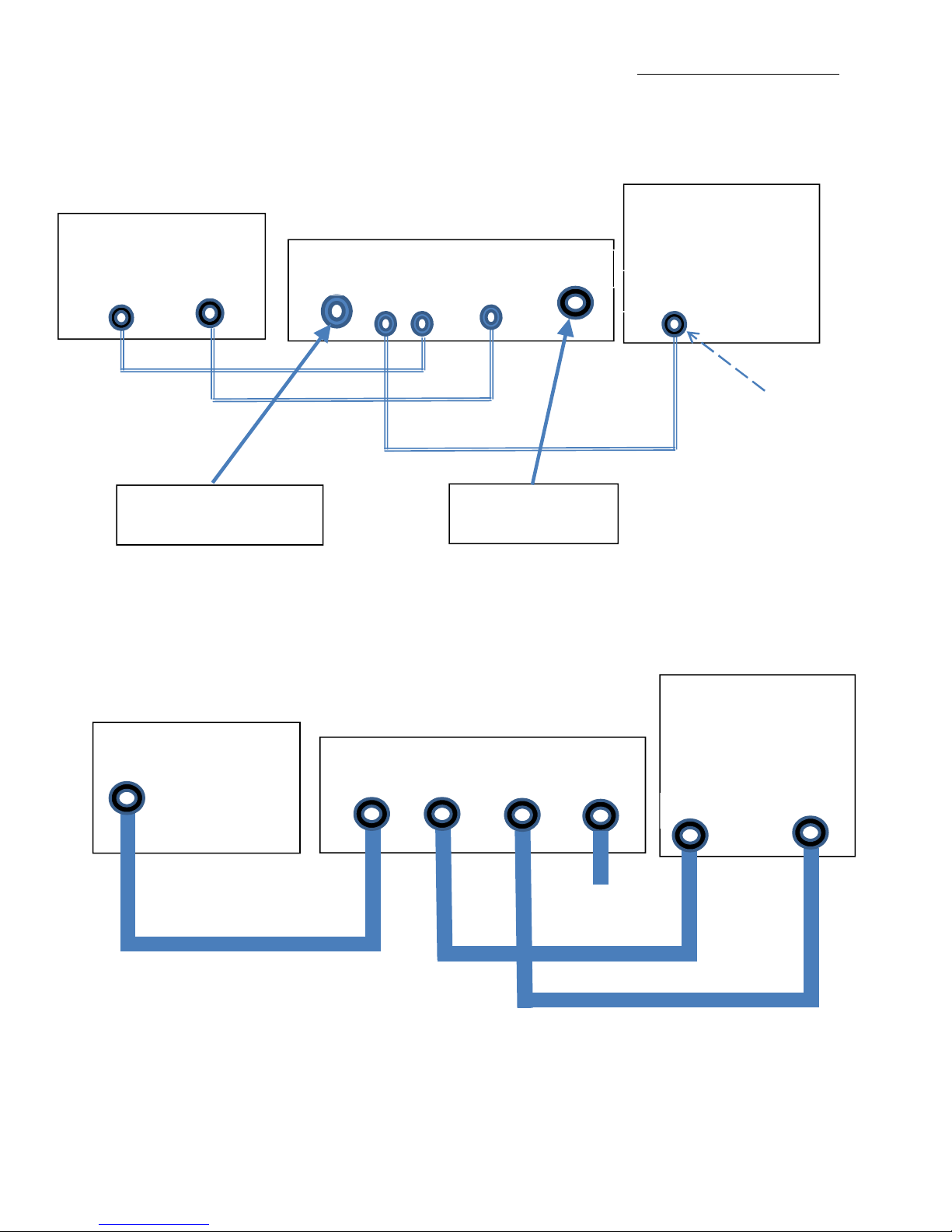
The Control interconnections are shown in Figure 1. The RF interconnections are shown in Figure 2.
Referring to Figure 1, the CW input device (i.e. key, paddle, bug, co puter, keyer, etc.) connects to the
¼” Key/Paddle stereo input jack on the QSK unit. For single line input devices such as a key, keyer, bug,
co puter CW, etc., a stereo jack ust still be used. The center pin is used for CW; the sleeve is left
unconnected. Paddles connect to the center pin and the sleeve in the nor al anner (dit center, dah
sleeve).
The delayed CW appears at the Xcvr Key/Paddle ini stereo jack on the QSK unit. This jack connects to
the Key/Paddle input on the transceiver.
The transceiver’s A plifier Key jack connects to the AMP Key IN phono jack on the front of the QSK unit.
The transceiver keys to ground a 5VDC 1 a signal fro the QSK unit. (Contact DX Connection to use
Kenwood’s +12 VDC for a plifier keying.) The QSK’s AMP Key OUT phono jack connects to the
a plifier’s AMP Key IN (or ‘antenna relay’, ‘T/R relay’, or ’trans it input’) as shown in Figure 1. It keys
the a p T/R relay to ground. No QSK setting changes are required for keying either positive or negative
a p T/R relay voltage polarity.
A 17 to 25 volt, 200 illia p, ‘wall wart’ type DC power supply connects to the ‘Pwr In’ jack on the front
panel. The power supply requires a 2.1 power plug (center positive).
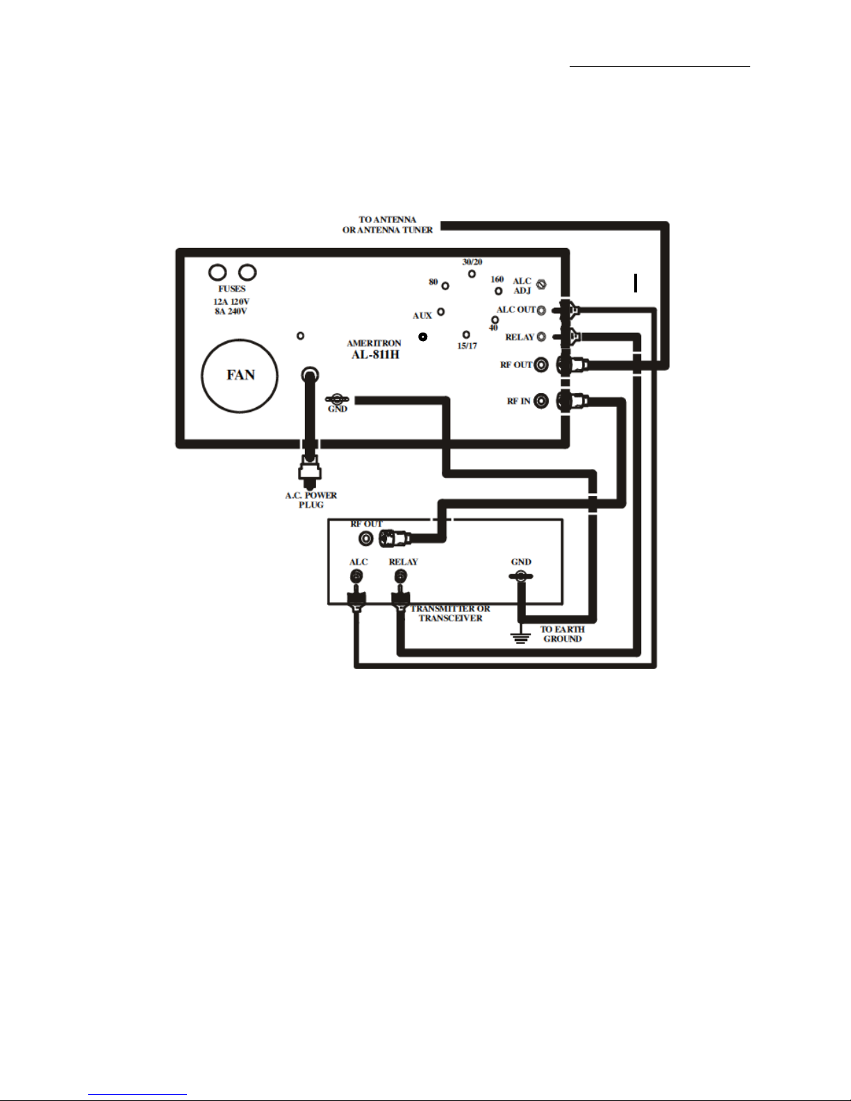
4) Example Interface to Ameritron AL-811 amplifier series
The QSK 2500© interface to the A eritron AL-811 series of a plifiers is shown in Figures 5, 6, and 7.
5) Operation
The QSK power switch places the unit in either (a) AMP ode or (b) ByPass ode. In AMP ode, the
QSK unit is active and perfor s the expected switching of the RF signal. The QSK unit must be in
AMP mode anytime that the amp ifier is to be used regard ess of the operating mode, i.e.
SSB, CW, RTTY, PSK, etc.
If the a plifier is not to be used, then the QSK unit can be set to ByPass ode which turns it’s DC power
off and routes the Key/Paddle input jack to the Xcvr Key/Paddle output jack. See Figure 3. The QSK
unit can be set to AMP ode for transceiver-only operation if the a plifier power is turned off or the
a plifier key input is disabled. So e a plifiers can be disabled by a switch on the front panel. For this
case, it is not necessary to set the QSK unit to ByPass to operate without the a plifier. However, the
a plifier RF ports ust re ain connected to the QSK unit.

DxConnection@frontier.com
10/1/15 Page 4 of 11
6) Adjusting Amplifier Keying Delay
After the last dit or dah of a trans ission, the a plifier is held keyed for a short ti e to prevent
excessing switching of the a plifier T/R relay. The no inal factory setting is for a 3 sec delay which
satisfies ost users. Faster CW operators tend to want shorter delays and slower operators tend to
want longer delays. This setting is not critical and is ainly a user preference. (It does not affect QSK
receive or trans it ti ing.) A 20-turn screw-adjustable potentio eter is located next to the PIC16F676
chip (see Figure 1a below). It allows setting the delay fro 2 sec to 10 sec. After adjusting the
potentiometer, the QSK2500 must be switched off and back on for the adjustment to take affect.
Method 1:
The safe ethod is to adjust the potentio eter a few turns with the QSK unit turned off, and then turn
it on to see how the delay ti e has changed. Be sure to re e ber (or write down) the direction of the
adjust ent and the nu ber of turns so you can esti ate which direction to turn the potentio eter
screw the next ti e and how any turns. The adjust ent is approxi ately linear.
Method 2:
Be careful to not short any of the PIC16F676 pins. The delay can be set with the QSK unit powered up by
easuring the voltage on pin 8 of the PIC 16F676, and according to the following for ula.
Potentio eter voltage = (desired delay in sec - 2.0sec)/10.1sec * 5.0volts
(Re e ber: The QSK unit ust switched off for the delay change to take affect.)
7) Optional Key/Paddle Delay timing
The factory setting for the delay fro the QSK2500© Key/Paddle Input jack to the key/paddle Xcvr
Output jack is 10 s. This value is suitable for ost a plifier/transceiver co binations. The user is
encouraged to use this setting unless this delay is known to be too short. Table 2 below shows that by
adding the appropriate solder ju pers, the ti ing can be adjusted fro 3 s to 16 s. There are pairs of
holes located next to pins 2, 3, and 4 of the PIC16F676 for the ju pers (see Figure 1a below ). (1/4”
bare #22 solid wire akes a suitable ju per.) The delay should not be lowered below 10 s unless test
equip ent is available to assure hot switching of the a plifier T/R relay does not occur at the start of
the first dit or dah of each trans ission.
Note: Many commercia externa QSK units (inc uding PIN diode types) do not protect against hot
amp ifier T/R re ay switching at the start of the first dit or dah of each transmission.
8) Limited Warranty
DX Connection warrants to the original purchaser that this product is free fro defects in aterial or
work anship for a 180 day period fro date of original purchase. This li ited warranty is for either the
repair or replace ent of the QSK unit only. There is no coverage for anything other than QSK unit. A DX
Connection Return Authorization (RA) is required for warranty service. E ail or ail a copy of the

DxConnection@frontier.com
10/1/15 Page 5 of 11
purchase receipt and a description of the proble to DX Connection to obtain a Return Authorization.
Upon receipt of the Return Authorization, return the unit shipping prepaid to DX Connection. DX
Connection will pay return shipping. 73
W. Rodgers K3HZP phone: (260) 432-8223
5727 Buckfie d Court
Fort Wayne, IN 46814 website: http://qsk2500.myfreesites.net/
Figure 1a Delay potentiometer & jumper holes by PIC processor

DxConnection@frontier.com
10/1/15 Page 6 of 11
Table 1 Total time for Amp T/R relay to switch
(factory delay setting= 10ms)
transceiver transceiver
RF de ay
QSK 2500©
key de ay
(factory setting)
total T/R
actuation
time
comment
Yaesu FT
-
1000MP MKV
5
s ( in)
10 s
15ms (min)
longer settings
in cvr
Elecraft K3
8 s ( in)
“
18ms (min)
“
“ “ “
Kenwood
TS
-
480, TS
-
2000
10 s
“
20ms
fixed in Xcvr
Ico IC
-
7000
10 s
“
20ms
“ “ “
Yaesu FTDX
-
9000, FT
-
2000
15 s
“
25ms
“ “ “
TenTec O niVII & Orion I/II
15 s
“
25ms
“ “ “
Ten Tec Eagle
17 s
“
27ms
“ “ “
ICOM IC
-
706
15 s
“
25ms
“ “ “
ICOM IC
-
735
5
.5
s
“
15
.5
ms
“ “ “
Table 2 Changing QSK timing delay (Optional)
(Jumper 2 adjacent holes together. They are next to the PIC16F676 pin specified in table.)
pin 2 pin 3 pin 4 QSK delay Comment
-
-
-
10 s
factory setting (no ju pers)
ju per
-
-
8 s
add 1 ju per
-
ju per
-
6 s
add 1 ju per
ju per
ju per
-
4 s
add 2 ju pers
-
-
ju per
3 s
add 1 ju per
ju per
ju per
12 s
add 2 ju pers
-
ju per
ju per
14 s
add 2 ju pers
ju per
ju per
ju per
16 s
add 3 ju pers

DxConnection@frontier.com
10/1/15 Page 7 of 11

DxConnection@frontier.com
10/1/15 Page 8 of 11
amp ifier
(back)
QSK 2500
©
(back
)
transceiver
(back)
transceiver
QSK 2500
©
(front)
amp ifier
out
key/paddle
IN
key, paddle, keyer
co puter, bug, etc.
key/paddle
key/paddle xcvr
Amp Key
A p Key
In
Amp Key
IN
Pwr In
RF OUT
RF IN
RF
OUT
antenna
RF IN
RF OUT
ANT
XCVR
Figure 2 RF Connections (back)
Figure 1 Control Connections (QSK 2500© front)
DC power: 17
-
25 volts
200 a
2 to +200 VDC to gnd or
-2 to -200 VDC to gnd;
100ma (max)

DxConnection@frontier.com
10/1/15 Page 9 of 11
Key/Paddle jack
cvr
Key/Paddle jack
17 – 25 volts DC
power to QSK
Figure 3 Circuit for power switch set to ‘Bypass’
input to QSK
A p out
A p in
Xcvr
Ant
Figure 4 RF circuit in ‘receive’ & ‘off’ states
X
c
v
r relay
control
B+
A p relay control
B+

DxConnection@frontier.com
10/1/15 Page 10 of 11
Figure 5 AL-811H without QSK 2500
Examp e: QSK 2500 interface to
AL
-
811H
Amp ifier

DxConnection@frontier.com
10/1/15 Page 11 of 11
RF IN
out
key/paddle
(in)
transceiver
QSK 2500
©
(front)
AL
-
811H
amp ifier
key/paddle
key/paddle xcvr
Relay
(back)
A p Key
In
Relay
Pwr In
transceiver
(back)
QSK 2500
©
(back
)
AL
-
811H
amp ifier
RF OUT
RF OUT
antenna
RF IN
RF OUT
ANT
XCVR
Figure 7 AL-811H RF Connections (ALC cable is unchanged)
Figure 6 AL
-
811H Relay connections
fan
fan
Other manuals for QSK 2500
1
Table of contents
Other DX Connection Amplifier manuals
Popular Amplifier manuals by other brands

Geemarc
Geemarc LOOPHEAR 10 user guide

Behringer
Behringer BASS V-AMP LX1B user manual

Musical Surroundings
Musical Surroundings THE PHONOMENA II + owner's manual

Artone
Artone PMS-260D user manual

Fuchs Audio Technology
Fuchs Audio Technology Overdrive Supreme ODS-30 Operation manual

ALLNIC AUDIO
ALLNIC AUDIO HA-3000 owner's manual