EACA EG 3014 User manual

EG 3014
EG 302
1
EXPANSION
TECHNICAL MANUAL

PREFACE
This manual is written to give abrief view of the theory of operation and technical information of
the Expander EG3014 and the optional interface boards that can be added to it. The manual can be
regarded as areference or areminder to the experienced technical people. It is expected that the reader
should have the basic knowledge of digital electronics in order to make full use of this manual.
Please do not hesitate to inform us about any errors, mistakes and information out of date. We are
pleased to correct the mistakes and up-date this manual.
1981

TABLE OF CONTENTS
1. EG3014 EXPANDER PAGE
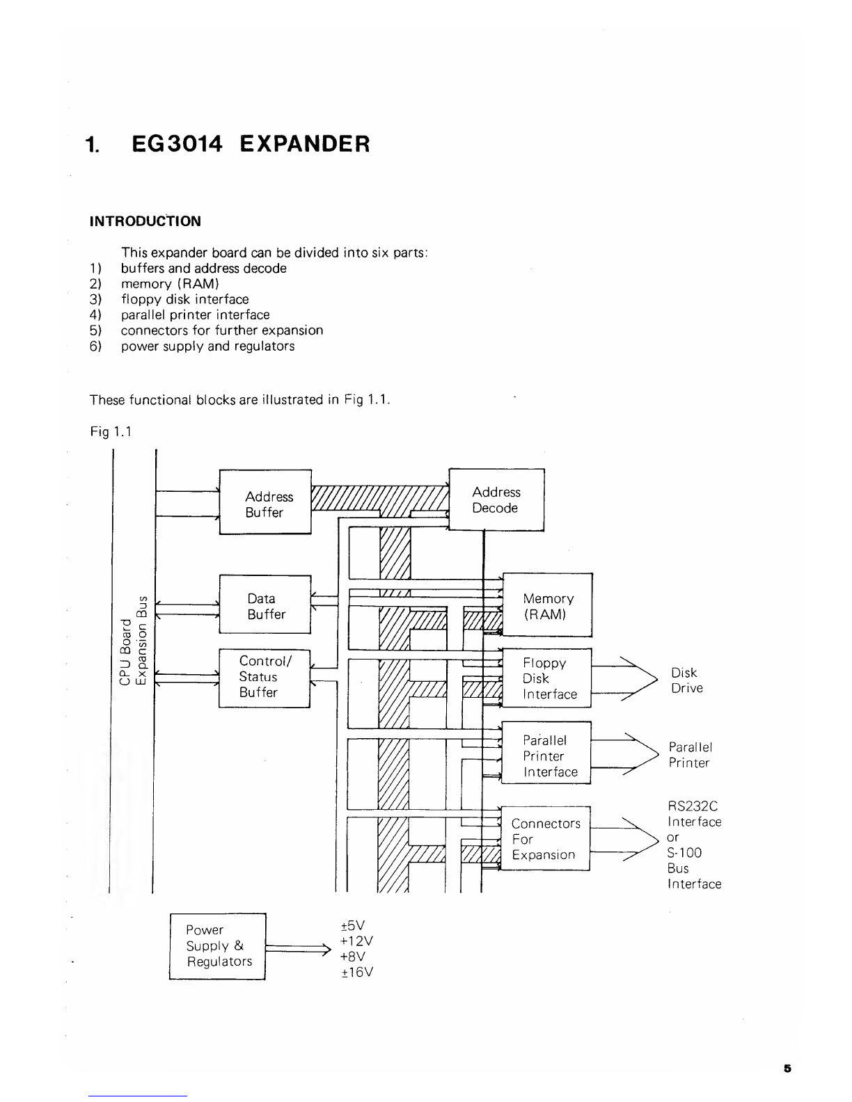
1.1 Buffers and Address Decode Logic __ _ ______.6
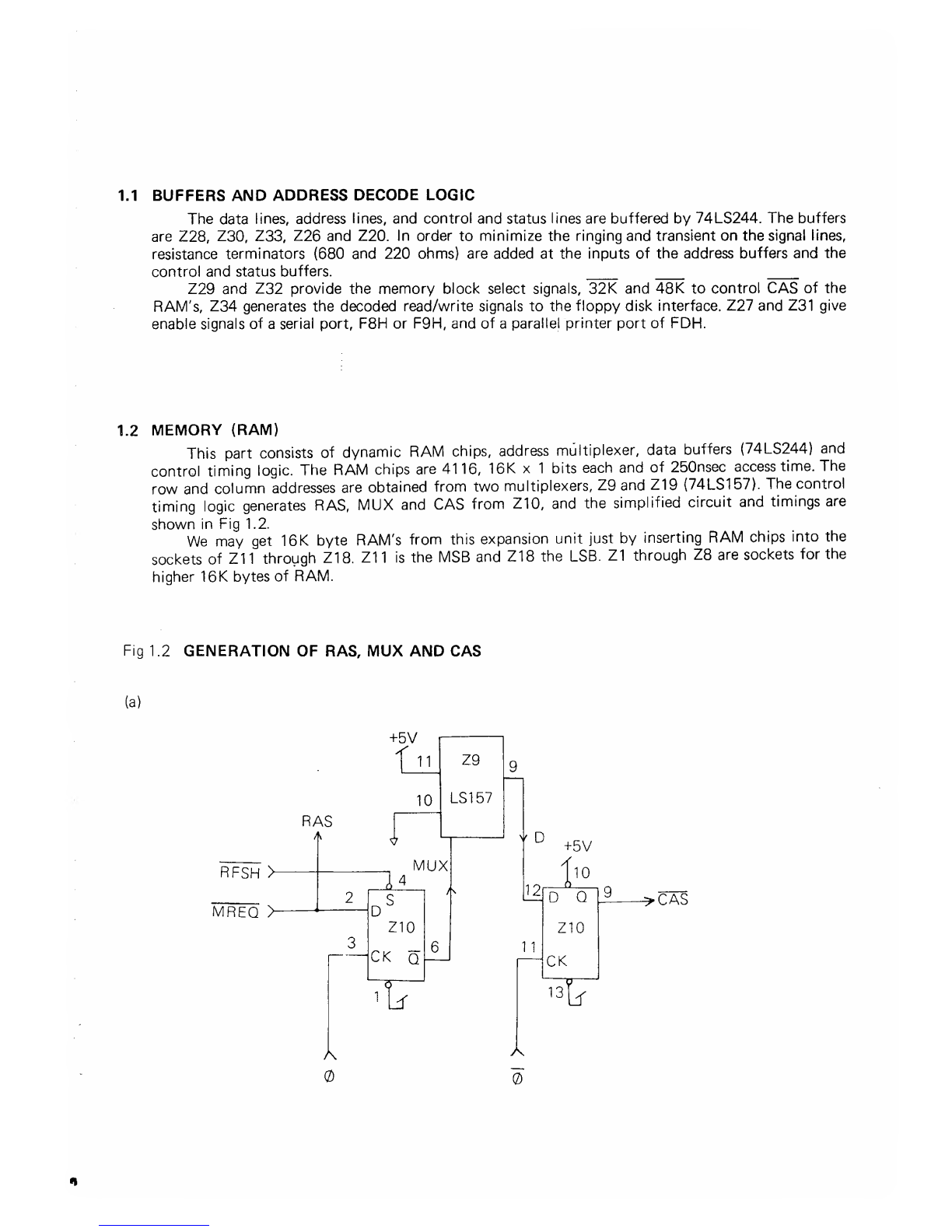
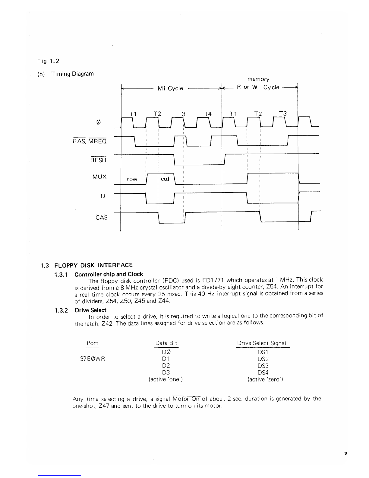
1.2 Memory (RAM) _____.____..____. 6
1.3 Floppy Disk Interface ________________ 7
1.3.1 Controller Chip and Clock __„__„___. 7
1.3.2 Drive Select __„„_„______. 7
1.3.3 Address Decode ____________ 8
1.3.4 Data Separation _____ ______. 8
1.3.4.1 Internal Data Separator __ _—__ _. __ _. 8
1.3.4.2 External Data Separator __„„____. 9
1.3.5 Side Select __. __ _ ______.11
1.3.6 Card-Edge Pin Assignemnt
for Floppy Disk Interface _—__„___ __ _.1
1
1.4 Parallel Printer Interface ____'„ ____ __.12
1.4.1 Printer Status _____„_____. 12
1.4.2 Card-Edge Pin Assignment
for Parallel Printer Interface —_______.12
1.5 Connectors for Further Expansion ________. .13
1.5.1 Pin Assignment for the 50-pin Connector ___. _„ „ .13
1.5.2 Pin Assignment for the 20-pin Connector —___—_.14
1.6 Power Supply and Regulators __ ____ ____ __.15
2. EG3020 RS-232-C INTERFACE ___ _ ___ ___.16
2.1 UART __„_____„____. 16
2.1.1 Control Bits ____-____ _ _.16
2.1.2 Clock __„________„. 16
2.2 Baud Rate Generator _____, -___ ___.17
2.3 Address Decode ____ ____ __.___. 17
2.4 TTL/E IALevel Shifters ___________ 18
2.5 Busses __-------_--_.18
2.5.1 Pin Assignment for the RS-232-C Bus _-_____.18
2.5.2 Pin Connections between the Expander and the RS-232-C Interface __ _.19
2.6 Voltage Regulator ___ ___ _ _ ____-.19
3. EG3021 DOUBLE DENSITY ADAPTER (FLOPPY DISK) _____.20
3.1 Introduction ______ _„____. 20
3.2 Floppy Disk Controllers ___________ 20
3.3 Chip Select Decode Logic and Multiplexer _____. __.20
3.4 16 MHz Clock Generator _„„_„„____. 21
3.5 Write Precompensation ___ _____ _ _ __ _.21
3.6 Data Separator ______ __ _ _ __.21
3.6.1 Single Density _. _____ ______ 21
3.6.2 Double Density __ _ _______ __.23
4. EG3022 S-100 BUS INTERFACE ____„___.24
4.1 introduction ___ _____ __ __ ___.24
4.2 Address Lines ____ —______ _ .24
4.3 Data Lines ____„_______ 24
4.4 Control/Status Lines _„_____ ____.24
4.5 Vectored Interrupt Lines __ „________.25
4.6 Power Lines _________ __ ____ .25

PAGE
4.7 Bus and Connector Pin Assignment ______ ___—.25
4.7.1 Pin Assignment for the 50-pin Connector between the Expander
and the S-100 Bus Interface Board. ------_.25
4.7.2 Pin Assignment for the Connectors between the S-100 Bus Interface
Board and the Mother Board. __— — — — -_26
4.7.2.1 50-pin PCB Solder-to-board Connector ____-.26
4.7.2.2 34-pin PCB Solder-to-board Connector —_—--.27
4.7.3 Pin Assignment for the S-100 Bus Connector on the Mother Board __.27
5. COMPONENT LAYOUT DIAGRAMS _____--_ -30
6. SCHEMATICS _„_____-----•35
APPENDIX A—Pin Connections between the Expander and the Video Genie System _.43

INTRODUCTION
The Expander EG3014 provides useful interfaces to the main unit of the Video Genie System. It
includes 32K bytes of dynamic RAM memory, floppy disk controller and interface, and parallel printer
interface. There are optional interface boards that can be added to the Expander. They are the RS-232-C
interface and S-100 Bus interface.
The circuits of these interfaces are described briefly part by part so that the users may understand
their Expander more quickly and modify it to suit their own use.

1. EG3014 EXPANDER
INTRODUCTION
This expander board can be divided into six parts:
1
)
buffers and address decode
2) memory (RAM)
3) floppy disk interface
4) parallel printer interface
5) connectors for further expansion
6) power supply and regulators
These functional blocks are illustrated in Fig 1.1.
Fig 1.1
ZJ
CQ
c
o
\n
C
Q.
X
CJ LU
Address Y//
Buffer
Data
Buffer
Control/
Status
Buffer
Address
Decode
Memory
(RAM)
Floppy
Disk
Interface
^
dParallel
Printer
Interface
Connectors
For
Expansion
"7^
_^
>Disk
Drive
Parallel
Printer
RS232C
Interface
or
S-100
Bus
Interface
Power
Supply &
Regulators
±5V
+12V
^+8V
±16V

1.1 BUFFERS AND ADDRESS DECODE LOGIC
The data lines, address lines, and control and status lines are buffered by 74LS244. The buffers
are Z28, Z30, Z33, Z26 and Z20. In order to minimize the ringing and transient on the signal lines,
resistance terminators (680 and 220 ohms) are added at the inputs of the address buffers and the
control and status buffers.
Z29 and Z32 provide the memory block select signals, 32K and 48K to control CAS of the
RAM's, Z34 generates the decoded read/write signals to the floppy disk interface. Z27 and Z31 give
enable signals of aserial port, F8H or F9H, and of aparallel printer port of FDH.
1.2 MEMORY (RAM)
This part consists of dynamic RAM chips, address multiplexer, data buffers (74LS244) and
control timing logic. The RAM chips are 4116, 16K x1bits each and of 250nsec access time. The
row and column addresses are obtained from two multiplexers, Z9 and Z19 (74LS157). The control
timing logic generates RAS, MUX and CAS from Z10, and the simplified circuit and timings are
shown in Fig 1.2.
We may get 16K byte RAM's from this expansion unit just by inserting RAM chips into the
sockets of Z11 through Z18. Z11 is the MSB and Z18 the LSB. Z1 through Z8 are sockets for the
higher 16K bytes of RAM.
Fig 1.2 GENERATION OF RAS, MUX AND CAS
(a)
RFSH >
MREQ >^CAS

Fig 1.2
(b) Timing Diagram
RAS, MREQ
RFSH
MUX
D
CAS
\
M1 Cycle
memory
J<—Ror WCycle H
T1 T2 T3 T4
row
/
col \
\r
T1 T2 T3
i
A_
r
1.3 FLOPPY DISK INTERFACE
1.3.1 Controller chip and Clock
The floppy disk controller (FDC) used is FD1771 which operates at 1MHz. This clock
is derived from a8MHz crystal oscillator and adivide-by eight counter, Z54. An interrupt for
areal time clock occurs every 25 msec. This 40 Hz interrupt signal is obtained from aseries
of dividers, Z54, Z50, Z45 and Z44.
1.3.2 Drive Select
In order to select adrive, it is required to write alogical one to the corresponding bit of
the latch, Z42. The data lines assigned for drive selection are as follows.
Port
37E0WR
Data Bit
D0
D1
D2
D3
(active 'one'
Drive Select Signal
DS1
DS2
DS3
DS4
(active 'zero')
Any time selecting adrive, asignal Motor On of about 2sec. duration is generated by the
one-shot, Z47 and sent to the drive to turn on its motor.

1.3.3 Address Decode
The address decode for this floppy disk interface is assigned as in Table 1.1.
Table 1.1
Control Signal
37E0RD
37E0WR
37ECRD
37ECWR
(active low)
Signal To
Interrupt Logic
Drive Select
Disk Controller
Disk Controller
Function
Read Interrupt Status
Select Drive®-
3
Read Data From Disk Controller
Write Data To Disk Controller
Transfer of data between the Disk Controller and CPU is accomplished by the following
signals in Table 1.2.
Table 1.2
Address
A1 A0
1
1
11
37ECRD 37ECWR
(RE) (WR)
Status Register Command Register
Track Register Track Register
Sector Register Sector Register
Data Register Data Register
1.3.4 Data Separation
1.3.4.1 Internal Data Separator
FD1771 provides an internal data separation by pulling HIGH the signals,
XTDS (pin 25) and FDCLOCK (pin 26). The raw READ DATA from the disk drive
is fed into FDDATA (pin 27 of FD1771). Note that FD1771 has the compatibility
of soft sectored recording format on the diskette.
Practical experience tells us that an external data separator is more reliable in
data recovery than the internal data separation. XTDS is pulled LOW to select
external data separation. The separated clock and data are fed into FDCLOCK and
FDDATA respectively.
In each case, select the jumpers J1 ,J3 and J4 referring to the schematics and
component layout diagram. Normally, these jumpers are connected in the mode of
external data separation.

1.3.4.2 External Data Separator
The external data separator can be simplified as in Fig 1.3a Fig 1.3b shows the
timings of the data separator.
Fig 1.3 EXTERNAL DATA SEPARATOR
a) Circuit
FROM
Z47-13 vREAD
DATA
Z55
cZ59 1r-.
tf> >- -»SEP DATA
">- i*SEP
CLOCK
Z59
9C
13
Z55
RLI
SQ- 10
3>13 1
FF1 FF3 Z56
>0.1
CK
R
>CK
Q3
R
11
23_
Z60
>->
SI
Q
Z59 Z56
13
10
S2
i> Q
R
11

Fig 1.3 EXTERNAL DATA SEPARATOR
(b) Timing Diagram
data address mark
+READ
DATA
c
f
)c
II
:c
tr*
)c))c
f
-* c)c
u
Xi-)c\
Sep. Data f
F
Sep. Clock [
\t
misi ;ing clo ck \
[i\
*
1
L1
S1
yr
FF1
i
FF2
>
FF3
1
1
S2 i\it
n
The raw READ DATA which are negative-going pulses pass through Z47
(one-shot). Positive-going pulses with width of about 200 nsec. are obtained from
output of Z47 (pin 13). Z55 forms adata window and aclock window. for
separating the data pulses and clock pulses. When Z56-5 is HIGH, the data window
is opened with the clock window closed, and when Z56-5 is LOW, the clock
window is opened with the data window closed.

Z56 (S2) is aone-shot with output pulse of 5ysec in width, and Z56 (S1 )has
pulse width of 4ysec. One-shot S2 is normally triggered by the falling edge of the
separated clock. S1 is triggered by the falling edge of the separated data. During the
missing clock period in case of data address mark, S2 is triggered to HIGH by the
falling edge of S1 .Therefore, the separation stays in sync through the missing clock
period. At the end of three missing clocks, FF3 (Z60) will go HIGH at the falling
edge of the separated data. In turn, S2 output will be reset to LOW, and this will
open the clock window. Fortunately, aseparated clock appears, and FF3 (Z60) is
reset to aLOW level again. S2 is released from reset, and will work normally to
control the clock and data windows.
1.3.5 Side Select
Since the Side Select signal is generated, double-sided drives can be used. One
double-sided drive will replace two single-sided drives. This Side Select signal is derived from
the Drive Select signals. For instance, jumpers in positions 2and 4at J5 are added. When Side
Select is HIGH, the Side of diskette corresponding to DS1 and DS3 respectively are accessed.
When Side Select is LOW, the sides of diskette corresponding to DS2 and DS4 respectively
are accessed.
1.3.6 Card-Edge Pin Assignment for Floppy Disk Interface
(Refer to the component layout diagram)
Pin
odd pins
2
4
6
8
10
12
14
16
18
20
22
24
26
28
30
32
34
Signal
GND
NC
NC
SIDE SELECT
INDEX/SECTOR
DS1
DS2
DS3
MOTOR ON
DIR SEL
STEP
WRITE DATA
WRITE GATE
TRACK 00
WRITE PROTECT
READ DATA
DS4
NC
Description
odd pins of 1through 33 all GND
To double-sided drives fr cirt on-t^
Input to FDC, active LOW
(Output from FDC,
(active LOW
(Drive Select 1,2and 3
Output from FDC, active LOW
Output from FDC, step out when HIGH,
step in when LOW
Output from FDC, active LOW-to-HIGH
Output from FDC, low going pulses.
Output from FDC, write data when LOW,
read data when HIGH
Input to FDC, active LOW
Input to FDC, low going pulses
Output from FDC, Drive Select 4, active LOW %ZidtStlect
-vroto\ QZ

1.4 PARALLEL PRINTER INTERFACE
This 8-bit printer port is of address FDH or 37E8H and is enabled by the decoded signal PPR.
The serial printer port, SPR, when LOW will disable this parallel printer port.
This Interface consists of a8-bit data latch, (Z48 and Z49) and abuffer (253) for the status
lines from the printer. There are also two one-shots (Z57); one generates the signal DATA STRB
which strobes the data into the register of aprinter, and the other generates apositive pulse at
Z52-13 to activate the BUSY line, bit 7of status lines. This positive pulse is generated just after the
data are clocked into the latch, and inhibits further data transfer from the CPU to the printer before
the printer sets the signal BUSY.
1.4.1 Printer Status
The status lines are assigned as below.
Bit
7
6
5
4
Status (active HIGH)
BUSY
OUT OF PAPER
DEVICE SELECTED
ALWAYS HIGH
1.4.2 Card-Edge Pin Assignment for Parallel Printer Interface
(Refer to the component layout diagram)
Pin Signal Pin
2
Signal
1DATA STROBE GND
3D0 4GND
5D1 6GND
7D2 8GND
9D3 10 GND
11 D4 12 GND
13 D5 14 GND
15 D6 16 GND
17 D7 18 GND
19 NC 20 GND
21 BUSY 22 GND
23 OUT OF PAPER 24 GND
25 UNIT SELECT 26 NC
27 NC 28 NC
29 NC 30 NC
31 NC 32 NC
33 NC 34 NC

1.5 CONNECTORS FOR FURTHER EXPANSION
on ThTD
eifre tW°connectors Provided on the expander board; one has 50 pins (P2) and the other
*ocoior. 5(>Pm connector mav be for S-100 bus interface board and the 20-pin connector
tor HbZ32C interface board. The positions of the connectors refer to the component layout diagram
1.5.1 Pin Assignment for the 50-pin Connector
Pin SIGNAL ACTIVE LEVEL DESCRIPTION
1+16V SEMI-REGULATED
2CLOCK 2MHz, 50% DUTY CYCLE
3-16V SEMI-REGULATED
4MEMDIS LHIGHEST 32K MEMORY
DISABLE
5+8V SEMI-REGULATED
6FX LRESERVED PORT ADDRESS
7D4 DATA BIT 4
8INTA LDATA IN ENABLE
9BD6 DATA BIT 6
10 BD5 DATA BIT 5
11 BD0 DATA BIT
12 BD7 DATA BIT 7
13 BD2 DATA BIT 2
14 BD1 DATA BIT 1
15 BA2 HADDRESS LINE 2
16 BD3 DATA BIT 3
17 BA0 HADDRESS LINE0
18 BA1 HADDRESS LINE 1
19 BA15 HADDRESS LINE 15
20 BA14 HADDRESS LINE 14
21 BA4 HADDRESS LINE 4
22 BA11 HADDRESS LINE 11
23 BA6 HADDRESS LINE 6
24 BA5 HADDRESS LINE 5
25 BA12 HADDRESS LINE 12
26 BA7 HADDRESS LINE 7
27 BA9 HADDRESS LINE 9
28. BA10 HADDRESS LINE 10
29 BA8 HADDRESS LINE 8
30 BA13 HADDRESS LINE 13
31 MASTER CLOCK, 1.8 MHz
32 BA3 HADDRESS LINE 3
33 PHLDA LPROCESSOR HOLD ACKNOWLEDGE
34 PINT LINTERRUPT REQUEST
35 HALT LPROCESSOR HALT ACKNOWLEDGE
36 PHANTOM LMEMORY DISABLE FOR
LBOOT-STRAPPING
37 IORQ I/O REQUEST CYCLE
38 PWAIT LPROCESSOR WAIT CONTROL
SIGNAL
13

PIN SIGNAL ACT IVE LEVEL
L
DESCRIPTION
39 WR PROCESSOR WRITE CYCLE
40 PHOLD LPROCESSOR HOLD CONTROL
LSIGNAL
41 CCDBS/STATDBS CONTROL SIGNALS AND STATUS
LDISABLE
42 DODBS/ADDBS DATA OUTPUTS AND ADDRESS
LINE DISABLE
43 NMI LNON-MASKABLE INTERRUPT
44 RESET LRESET CONTROL SIGNAL
45 M1 LOP-CODE FETCH CYCLE
46 RFSH LREFRESH CYCLE
47 MREQ L-MEMORY REQUEST CYCLE
48 RD LPROCESSOR READ CYCLE
49 GND
50 GND
1.5.2 Pin Assignment for the 20-pin Connector
PIN SIGNAL ACTIVE LEVEL
1BD5
2BD4
3BD7
4BD6
5BD1
6BD0
7BD3
8BD2
9BWR
10 BAO
11 BRD
12 SRESET
13 8MHz<2
14 SP*
15 -16V
16 PPR
17 +12V
18 +5V
19 SPR
20 GND
L
H
H
L
DESCRIPTION
DATA BIT 5
DATA BIT 4
DATA BIT 7
DATA BIT 6
DATA BIT 1
DATA BIT
DATA BIT 3
DATA BIT 2
PROCESSOR WRITE CYCLE
ADDRESS LINE0
PROCESSOR READ CYCLE
SYSTEM RESET
8MHz, 50% DUTY CYCLE
SERIAL PORT SELECT
SEMI-REGULATED
PARALLEL PRINTER PORT
SELECT
REGULATED
REGULATED
PARALLEL PRINTER DISABLE
GROUND
14

1.6 POWER SUPPLY AND REGULATORS
The power supply provides three semi-regulated output voltages: +8V, +16V and —16V.
The specifications for these voltages are as follows:
Voltage No Load Voltage Full Load Voltage Remark
min. max. min. max.
+16V 20V 24V 15V 18V F.L. +16V@1 50mA
-16V 20V 24V 15V 18V F.L. -16V@100mA
There are three voltage regulators on the expander board. IC regulators 7805 (Z62) and 7812
(Z61 )are used to supply +5V and +12V respectively. Asimple regulator with transistor 03 and 5.6V
zener diode regulates -16V to obtain -5V supply for the RAM's and FD1771.

2. EG3020 RS-232 INTERFACE
This RS-232-C Interface is an optional board to be plugged into the 20-pin connector (P1) of
EG3014 expander. This board consists of six parts:
1. UART
2. Baud rate generator
3. Address decode
4. Level shifters
5. Busses
6. Voltage regulator (-12V)
2.1 UART
The UART chip used is TR1863 or AY-3-1014A which needs single +5V supply. It has 8
received data lines output to the CPU and 8data lines input to the UART. The serial data format can
be determined by properly setting the control bits. This can be done by turning ON or OFF the dip
switches, SI -S5 of DP1.
2.1.1 Control Bits
(ON ='0' and OFF
2.1.1.1
2.1.1.2
2.1.1.3
2.1.1.4
'1')
No Parity (NP)
ogic
1
S1: parity
with parity bit
no parity bit added
Number of stop Bits (TSB)
S2: logic stop bit
~W 1
12
11Vi if 5bits/character is selected.
Number of Bits/Character (NB2, NB1)
S3: NB2 S4
1
1
Odd/Even Parity Select
S5: logic
1
NB1 Bits/Character
5
16
7
18
t(EPS)
pairty
odd
even
2.1.2 Clock
The transmitter and the receiver use the same clock whose frequency is 16 times the
desired baud rate.
ia

2.2 BAUD RATE GENERATOR
The baud rate is obtained by dividing the 8MHz clock, and has eight choices from 110 to
19200 baud. They can be selected by flipping the switches of DP2. Z10and Z11 (74LS161) are
programmed to be divide-by 11and divide-by 13 respectively.
2.3 ADDRESS DECODE
The address decode is accomplished by Z1 (74LS138). SP* is aserial port enable signal with
addresses F8 and/or F9. See Table 2.1. If S7 of DP1 is ON, aserial printer mode is selected, and SPR
is the signal fed back to the expander board to disable the parallel printer interface.
Table 2.1 Address Decode
PORT ADDRESS INPUT TO CPU OUTPUT TO INTERFACE
SERIAL INPUT F8H DATA STATUS
SERIAL OUTPUT F9H STATUS DATA
SERIAL PRINTER FDH STATUS DATA
The mode of operation can be chosen as below.
DP1
MODE S6 SZ S8
Serial Printer OFF ON OFF
Communication ON OFF ON
The bit assignment for status ports is illustrated in Table 2.2
Table 2.2
DATA
BIT
D0
D1
D2
D3
D4
D5
D6
D7
STATUS PORTS
COMMUNICATION
OUT PORT F8H
Request-to-send
Data Terminal
Ready
UART reset
1=true
unused
unused
unused
unused
unused
IN PORT F9H
Data Available
1=true
Overrun Error
1=true
Framing Error
1=true
Parity Error
1=true
Carrier Detect
Data Set Ready
Clear-to-send
Transmitting
Buffer Empty
=true
SERIAL PRINTER
IN PORT FDH
unused
unused
unused
unused
Carrier Detect
Data Set Ready
Always LOW
Transmitting
Buffer Empty
0= true
17

2.4 TTL/EIA LEVEL SHIFTERS
Drivers/level shifters are required to interface this RS232-C interface with data communication
equipment. El ARS232-C standard specifies that signal voltage levels should have threshold of ±3V.
Logic 'V or OFF means signal voltage less than —3V, and logic '0' or ON means signal voltage greater
than +3V.
Driver 1488 (Z2) with ±Vcc of ±12V is used for signals output to the RS-232-C bus. Line
receiver 1489 (Z3) is used for signals inputs from the RS-232-C bus to the interface board.
2.5 BUSSES
2.5.1 The pin assignment for the RS-232-C Bus is as follows:
PIN SIGNAL DESCRIPTION
1PGND Protective Ground
2TXD Transmit Data (OUT)
3RXD Receive Data (IN)
4RTS Request-to-send (OUT)
'ON' —peripheral to transmit data
'OFF' —peripheral to receive (or non-transmit)
5CTS Clear-to-send (|[\|)
'ON' —peripheral can receive data.
'OFF' —no data should be transferred.
6DSR Data Set Ready (IN)
'ON' —peripheral handshaking completed
'OFF' —handshaking not ready
7SGND Signal Ground
8CD Carrier Detect (IN)
'ON' —peripheral is receiving acarrier
'OFF' —no carrier is received
or the signal is too bad for data recognition
20 DTR Data Terminal Ready (OUT)
'ON' —peripheral should be connected to the communication
channel.
'OFF' —remove connection to the channel
18

2.5.2 Pin connections between the Expander and this RS-232-C Interface:
DFSCRIPTION
_PJN SIG NAL
1BD5
2BD4
3BD7
4BD6
5BD1
6BD0
7BD3
8BD2
9BWR
10 BA0
11 BRD
12 SRESET
13 8MHz0
14 SP*
15 -16V
16 PPR
17 +12V
18 +5V
19 SPR
20 GND
DATA BIT 5
DATA BIT 4
DATA BIT 7
DATA BIT 6
DATA BIT 1
DATA BIT
DATA BIT 3
DATA BIT 2
PROCESSOR WRITE
ADDRESS LINE®
PROCESSOR READ
SYSTEM RESET
8MHz, 50% DUTY CYCLE
SERIAL PORT SELECT
SEMI-REGULATED
PARALLEL PRINTER PORT SELECT
REGULATED
REGULATED
PARALLEL PRINTER DISABLE
GROUND
2.6 VOLTAGE REGULATOR
+5V and +12V have been regulated on the expander board. -12V supply is required for the
level shifter 1488. So, asimple regulator with Q1 (9012) and a13V zener diode is used to supply
—12V from the semi-regulated —16V.
This manual suits for next models
3
Table of contents
Popular Extender manuals by other brands

Austin Hughes
Austin Hughes CyberView CV-K101 user manual

Nikrans
Nikrans LCD500-4G-D quick start guide

Avenview
Avenview HDM-SHAREPRO-IP user guide

StarTech.com
StarTech.com ST121HD20V quick start guide

Safeguard Supply
Safeguard Supply LRA-EXTX-L owner's manual

Espa
Espa AQUABOX 350 Acuaplus operating instructions