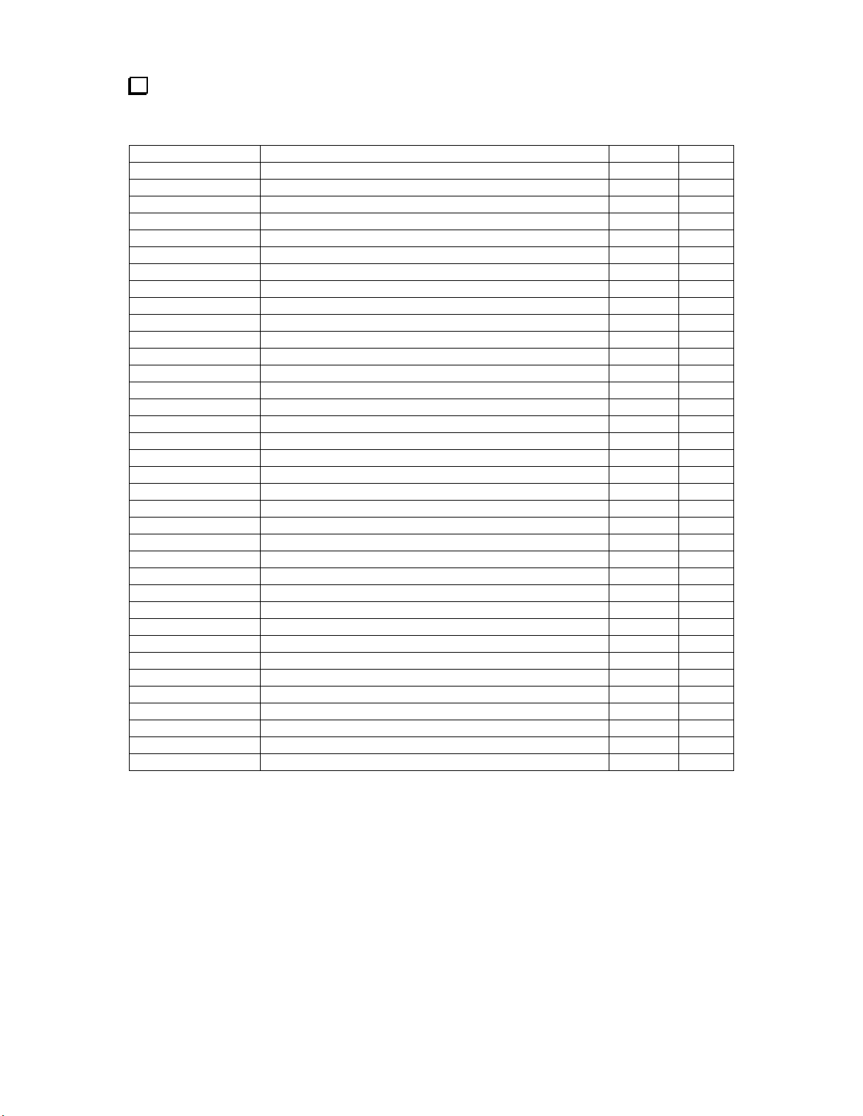
ELECRAFT KFL1-4 User manual

Elecraft • www.elecraft.com • 831-763-4211
ELECRAFT KFL1-4 FOUR-BAND FILTER BOARD
Assembly and Operating Instructions
Revision B, December 7, 2011. Copyright © 2011, Elecraft; All Rights Reserved
Important Manual Note
Assembly, alignment, and other information about the 4-band Filter board is covered in this manual, not in
the K1 Owner's Manual. Wherever the owner's manual mentions the 2-band module, you'll need to refer to
the applicable sections of this manual instead.
Please read the K1 Owner's Manual Errata Sheet now and make all corrections listed. The errata
sheet provides notations that will tell you when to refer to the KFL1-4 manual. Also, if you're just starting
to build your K1, read the first three chapters of the owner's manual before assembling this board.
Introduction
The KFL1-4 Filter board provides four of the most popular HF QRP bands on a single plug-in module: 40,
30, 20, and either 17 or 15 meters. The KFL1-4 is the same size as the 2-band K1 filter board (KFL1), and
can simply be plugged into the K1 transceiver with no other required changes.
The 4-band filter board is fully compatible with the KBT1 battery option and the KAT1 automatic antenna
tuner (ATU). With most antennas, the ATU will find a good match on all four bands.
The KFL1-4 covers the frequency ranges listed below. These ranges are approximate, and depend on which
VFO range the builder chooses during assembly (80 or 150 kHz). The builder must also select either 17 m
or 15 m band coverage. These topics are covered later in the manual.
Band 80 kHz VFO Range 150 kHz VFO Range
40 m 7.0-7.08 7.0-7.15
30 m 10.1-10.18 10.0-10.15
20 m 14.0-14.08 14.0-14.15
17 m 18.05-18.13 18.05-18.20
15 m 21.0-21.08 21.0-21.15
iCaution: Some parts in this kit can be damaged by static discharge or by dropping them
onto a hard surface. Before handling the integrated circuit (U1), put on an anti-static wrist strap, or
touch a grounded, unpainted metal surface. When handling crystals and toroid cores, be careful not
to drop them onto a hard surface.

2
Parts Inventory
The table below lists all parts in four-band filter board kit. The photographs in Appendix A of the K1
owner's manual may be helpful in identifying components. If anything is missing, contact Elecraft.
Note: Some capacitors use lettered reference designators, e.g. "CA". This is explained later in the manual.
Ref. Descri
p
tion Part No.
Q
t
y
C9 Capacitor, 2 pF ("2") or 2.2 pF ("2r2") E530047 1
CJ Capacitor, 2.7 pF ("2r7") or 3.3 pF ("3r3") E530065 1
C10, CK Capacitor, 4.7 pF ("4r7") or 5 pF ("5") E530048 2
C22, C26 Capacitor, 27 pF ("27" or "270") E530060 2
C29, C33 Capacitor, 56 pF ("56" or "560") E530015 2
C11-C14 Capacitor, 68 pF ("68" or "680") E530007 4
C24 Capacitor, 82 pF ("82" or "820") E530038 1
C21, C27, CN, CP Capacitor, 100 pF ("101") E530034 4
CL, CM Capacitor, 120 pF ("121") E530041 2
C31 Capacitor, 150 pF ("151") E530049 1
C23, C25 Capacitor, 180 pF ("181") E530008 2
C28, C34 Capacitor, 330 pF ("331") E530043 2
C30, C32 Capacitor, 560 pF ("561") E530052 2
C19, C35-C45 Capacitor, .001 µF ("102"), 0.1" lead spacing E530074 12
C15, C16, C17 Capacitor, .047 µF ("473") E530025 3
C46 Capacitor, 0.1 µF ("104"), 0.1" lead spacing E530020 1
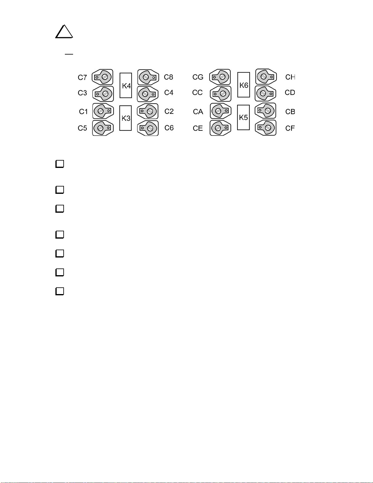
C1-C8,CA-CH Trimmer capacitor, 1-40 pF E540002 16
J1 Conn., 3-pin female E620009 1
J2 Conn., 10-pin female (dual row, 5 pins per row) E620045 1
K1-K8 Miniature DPDT relay E640010 8
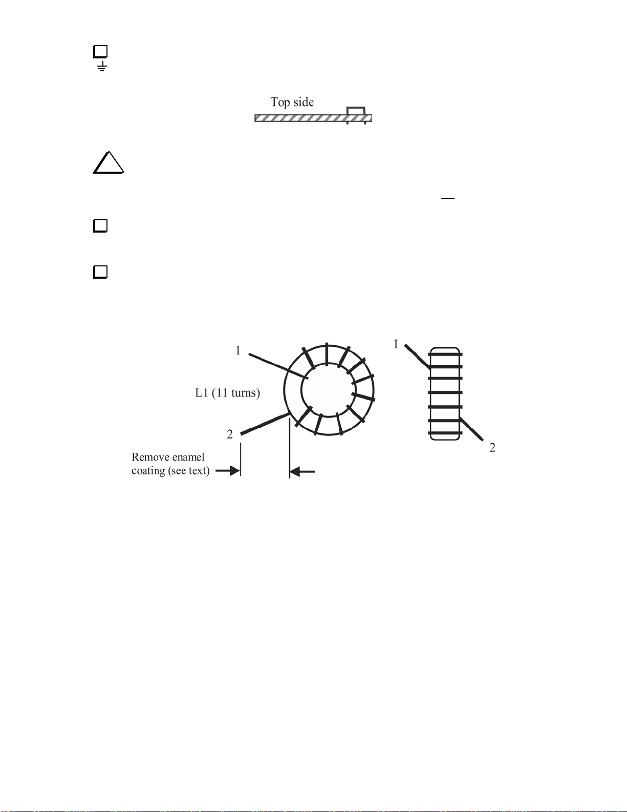
L1-L6, T1-T4 Toroidal inductor, T37-6 core (see text) E690013 10
P1, P2, P3 Conn., 8-pin male E620004 3
R1 Resistor, 100 ohms, 1/4 watt, 5% (brown-black-brown) E500010 1
RFC1 RF Choke, 100 µH (brown-black-brown; larger than R1) E690004 1
U1 IC, programmed microcontroller, PIC16C621A-04/P E610010 1
X1A Crystal, 29.000 MHz (for 21.0 MHz band) E660005 1
X1B Crystal, 26.050 MHz (for 18.0 MHz band) E660012 1
X2 Crystal, 22.000 MHz (for 14.0 MHz band) E660004 1
X3A Crystal, 18.100 MHz (for 10.1 MHz band) E660010 1
X3B Crystal, 18.000 MHz (for 10.0 MHz band) E660007 1
X4 Crystal, 15.000 MHz (for 7.0 MHz band) E660008 1
Z1 Ceramic resonator, 4 MHz E660001 1
Misc. Socket for U1 (18 pins) E620031 1
Misc. PC board, KFL1-4 E100129 1
Misc. Wire, #26 enamel, red E760002 12 ft
Misc. Wire, #26 enamel, green E760004 4 ft.

3
Firmware Requirements
The KFL1-4 four-band Filter board does not require upgraded K1 firmware to operate. The main
microcontroller in the K1 (U1 on the Front Panel board) will recognize whether a 2- or 4-band filter board
is present at power-on.
The KAT1 (automatic antenna tuner option) firmware will also work with the 4-band module.
Filter Board Assembly
iA fine-point, temperature-controlled soldering iron or soldering station (700-800 degrees F)
is strongly recommended to assemble the KFL1-4 PC board. If you don't have a soldering station, check
our web site (Builder Resources page) for suggested models. A higher-wattage iron or one with a wide tip
may damage components, pads, or traces.
Locate the KFL1-4 PC board and identify the top and bottom sides. The side of the board with the
label "KFL1-4" is the top.
Orient the board so that the top side is facing up. The large notch in the board should be to the lower
right.
Locate the position of resistor R1, along the front edge of the board (top side). The label "R1" appears
to the right of the resistor's outline.
Install a 100-ohm resistor (brown-black-brown) at R1. (Don't confuse it with RF choke RFC1, which
is larger.) Make sure it is seated flat on the board, then bend the leads outward slightly to hold it in place.
Solder R1 from the bottom side of the board. Then trim the leads as close as possible to the solder
joints.
Note: Many builders prefer to trim leads before soldering. Either order will work.

4
iThe approximate locations of the 16 trimmer capacitors on the Filter board are shown in Figure 1.
Relays K3-K6 are shown for reference. Note that each trimmer's body has a narrow end, and that they
are not all oriented in the same direction. The trimmers must be oriented as shown to keep their rotor
terminals at ground potential. This will allow them to be aligned with a metallic tool.
Figure 1
Install trimmer capacitors C1-C8 and CA-CH with their narrow ends oriented as indicated above
(toward the flat side of the outline on the pc board). Each trimmer must be gently pressed down as far as it
will go, but be careful not to bend the leads.
Solder all of the trimmer capacitors. Use just enough heat and solder to produce a clean, shiny solder
joint (and fill the hole). It should take no more than 2-3 seconds to solder each lead. Do not trim the leads.
Place relays K1-K8 at their indicated locations. DO NOT bend the relay leads to hold the relays on
the board, as this can cause mechanical stress. Note that the relays can only be installed one way due to
a gap between pins.
Carefully flip the board over, using a hardcover book to hold the relays in place. Make sure none of
the relays have fallen out, and that their leads are fully inserted into their PC board holes.
Solder just two pins (at opposite corners) on each relay, using a minimum amount of solder. Limit
soldering time to 2 or 3 seconds per pin to avoid damaging the relays.
Look at the relays from the top side of the board. If any of them are not fully seated onto the PC board,
re-heat the pins one at a time and gently press the relays down.
Solder all remaining relay pins. Do not trim the leads.

5
iWhen handling capacitors in the following steps, do not pull on the leads or bend them
excessively, since they can be quite fragile. In the case of capacitors with pre-formed leads, there is no
need to remove any bends. The short, pre-formed portion of the leads can remain exposed (above the
board) after installation.
Sort all of the capacitors, arranging them by value. This will make it easier to locate the correct
capacitor values during assembly. (Some small capacitor values may be labeled in more than one way. This
is explained page 9 of the K1 Owner's Manual. Also refer to the parts list, which shows alternate labeling.)
Install the capacitors listed below, but do not solder yet. Complete one row of the list before moving to
the next (the arrows in the list serve as a reminder). Start with capacitor C13 (68 pF), which is located near
the left end of the PC board, then go on to C11, C9, etc.
__ C13, 68 ("68") __ C11, 68 ("68") __ C9, 2 pF ("2") or 2.2 pF (2r2)
__ C12, 68 ("68") __ C14, 68 ("68")
Using the list above, double-check each capacitor's value. This step should not be skipped, since it
may be difficult to remove capacitors after they are soldered in place.
Trim and solder the leads of all capacitors installed so far.
C10 may be 4.7 pF ("4r7"), or 5 pF ("5"). To locate the position for C10, first find relays K2 and K3.
C10 is directly between the two. Install C10, then trim and solder.
Install the capacitors listed below, which are separated into three groups. After installing all the
capacitors in a group, double-check the values, then trim and solder the leads.
__ CL, 120 ("121") __ CM, 120 ("121") __ CN, 100 ("101")
__ CP, 100 ("101") __ CJ, See note 1 below __ CK, See note 2 below
__ C15, .047 ("473") __ C16, .047 ("473") __ C17, .047 ("473")
__ C43, .001 ("102") __ C44, .001 ("102") __ C45, .001 ("102")
__ C21, 100 ("101") __ C22, 27 ("27") __ C23, 180 ("181")
__ C24, 82 ("82") __ C25, 180 ("181") __ C26, 27 ("27")
__ C27, 100 ("101")
__ C28, 330 ("331") __ C29, 56 ("56") __ C30, 560 ("561")
__ C31, 150 ("151") __ C32, 560 ("561") __ C33, 56 ("56")
__ C34, 330 ("331")
Notes:
1- CJ may be 2.7 pF ("2r7") or 3.3 pF ("3r3").
2 - CK may be 4.7 pF ("4r7") or 5 pF ("5").

6
Install the capacitors listed below, which are all located on the bottom side of the board. Do not solder
yet.
__ C46, 0.1 ("104") __ C42, .001 ("102") __ C41, .001 ("102")
__ C40, .001 ("102") __ C39, .001 ("102") __ C38, .001 ("102")
__ C37, .001 ("102") __ C19, .001 ("102") __ C36, .001 ("102")
__ C35, .001 ("102")
Bend and trim the leads of the capacitors just installed. When soldering them, be very careful not to
touch any of the top-mounted components with the soldering iron (especially relays). If necessary, bend the
top-mounted capacitors slightly to keep them out of the way.
Install a 100-µH RF choke (brown-black-brown) at RFC1, on the top side of the board. Form the leads
of RFC1 using long-nose pliers to fit between the indicated pads. Trim the leads and solder.
Install an 18-pin IC socket at U1, with the notched end of the socket toward the notched end of the
IC's PC board outline. Bend two leads of the socket slightly to hold it in place while soldering. (U1 itself
will be installed in a later step).
Install the ceramic resonator, Z1. (Z1 looks like a capacitor with three leads, and can be oriented in
either direction.) Limit soldering time to 2 or 3 seconds on each pin to avoid altering Z1's oscillation
frequency. Trim Z1's leads after soldering.
iBefore crystals X1-X4 can be installed, you’ll need to choose whether to set up your K1 for 80-
kHz or 150-kHz VFO coverage1. The 80 kHz range covers the most-used portion of each CW band, and
will provide slightly smoother tuning. Refer to the Frequency Ranges table on page 1 of this manual for
details.
Indicate your VFO range selection here for reference: ___ 80 kHz ___ 150 kHz
Also note your selected VFO range on page 12 of the owner's manual (right column).
Two different crystals, X3A and X3B, are supplied for the 30 meter band. Identify the appropriate
crystal using the table below, and store the unneeded crystal. (X3 will be installed in a later step.)
VFO Range Lower Band Edge Crystal
80 kHz 10.100 MHz X3A (18.100 MHz)
150 kHz 10.000 MHz X3B (18.000 MHz)
1If your K1 is already assembled, use the VFO range you recorded on page 12 of the owner's manual.

7
Two different crystals, X1A and X1B, are supplied for the highest-frequency band, which can be
either 15 or 17 meters (21.0 or 18.05 MHz, respectively)2. Identify the desired crystal using the table
below, and store the unneeded crystal. (X1 will be installed in the next step.)
Band Crystal
15 meters X1A (29.000 MHz)
17 meters X1B (26.050 MHz)
Install the four crystals at X1-X4, but do not solder yet (crystal locations are shown in Figure 2). Be
sure to use the correct crystals at X1 and X3 based on your selections in the two previous steps. Orient the
crystals so that the marked frequencies can be read on all four. Bend the leads to hold them in place.
Figure 2
Re-check the crystal frequencies, then solder and trim the leads.
Cut four 1/2" (12 mm) bare wires. Solid hookup wire or discarded component leads can be used.
Referring to Figure 2, insert bare wires into the grounding holes provided near each crystal. Fold each
wire over the top of the crystal and solder it on top. Keep soldering time below 5 seconds at a time; if it
takes longer, your iron may not be hot enough, or your iron tip may not be making good contact with the
crystal can. Solder and trim the wires on the bottom of the board.
2Both bands are excellent choices for QRP operation. 15 meters is a low-noise, long-haul DX band with a
large CW segment, and is popular during contests, including Field Day. 17 meters is also excellent for DX
work, although it has a smaller CW segment. Like the other WARC bands (30 and 12 m), 17 m cannot be
used during contests.

8
At the ends of the board you’ll find two short jumper locations, each labeled with a ground symbol
(). Use component leads to make 3/4" (19 mm) U-shaped wires for each jumper (see Figure 3). Solder
the jumpers on the bottom side, keeping the top of the U-shape approx. 1/4" (6 mm) above the board.
Figure 3
iIn the following steps you’ll prepare and install several toroidal inductors. Winding the
toroids is not difficult. However, they must be wound exactly as indicated in the instructions, or the
transceiver will not operate correctly. Use only the number of turns specified. It is not necessary to use
an inductance meter to precisely match the inductances shown on the schematic.
All the toroid cores used on the KFL1-4 board are type T37-6 (yellow, 0.37" [19 mm] in diameter). If
you aren't yet familiar with toroidal inductors, please read the information on page 13 of the K1 owner's
manual titled "Identifying Toroid Cores."
Locate the component outline for inductor L1 at the right end of the Filter board, near C21. Compare
this component outline to Figure 4, which shows two views of L1. In the next few steps you'll wind L1 and
prepare its leads, then mount it vertically as shown in the drawing at the right. Note: Leads 1 and 2 of L1
are identified for use in winding instructions, but are not printed on the PC board.
Figure 4

9
Cut a 9" (23 cm) length of the red enamel-coated wire.
To wind L1, "sew" the long end of the wire through the core 11 times, spacing the turns as shown in
the left-hand drawing of Figure 4. Each pass through the core counts as one turn. Leave at least 1/2" (12
mm) of extra wire for each lead, and trim off the excess.
Hold L1 as shown in Figure 4. Verify that lead 1 of L1 terminates on the top side of the core and lead
2 terminates on the bottom. This winding sense (or direction) is required to match the pads provided for L1
on the PC board.
Make sure that the turns of L1 are evenly spaced, and that they occupy about 80% of the core. The
winding must look identical to Figure 4, with exactly 11 turns. (Always count toroid turns on the inside of
the core to make sure you're counting passes through the core.)
iAbout 90% of all problems with kits are caused by toroid leads that are not prepared
properly. We've made it as easy as possible by supplying "Thermaleze" heat-strippable enamel-coated
wire, but you'll need to do the rest. If you read and follow these instructions carefully, you'll avoid possible
frustration, troubleshooting, and repair charges.
The goal in preparing toroid leads is to (1) remove ALL of the enamel coating on the leads; (2) tin the leads
so that a clean solder joint will result. Leads must be tinned up to the edge of core (the core itself is non-
conductive). Review Figure 4, which shows the part of the leads to be stripped and tinned.
If you have a padded vise (such as a Panavise), clamp L1 into it with its leads horizontal, ready for
heat-stripping and tinning. (Don't over-tighten the vise as this might crack the toroid core.) If you don't
have a vise, lay L1 on a flat surface with one lead bent upwards slightly.
Melt a very small amount of solder (a "blob") onto your iron tip, then place the tip and the hot solder
in contact with the toroid lead, about 1/4" (6 mm) away from the core. If the iron is hot enough, you should
see the insulation bubble and start to vaporize after 4 to 6 seconds. Remove the iron when this occurs.
Clean the iron tip completely using a damp sponge. Then hold it back up to the lead to clean off any
residual solder. Use solder wick if necessary.
Examine the lead closely using a magnifying glass; you should see bare copper wire where the enamel
was removed. If any enamel coating remains, repeat the heat-stripping procedure. An alternative is to use
sandpaper. The lead must be free of all enamel before continuing.
Tin the lead by applying a small amount of fresh solder. The solder should appear clean and shiny. If it
looks dull or is not adhering very well to the bare lead, repeat the heat-stripping procedure.
Prepare the other lead of L1 in the same manner.

10
Install L1 vertically as shown by its component outline. Pull the leads taut on the bottom of the board
and bend them slightly to hold the toroid in place. Use the magnifying glass again to verify that the part of
each lead that extends from the pad is tinned and shiny. (If not, you will not be able to solder the lead
properly. Remove L1 and re-do lead preparation.)
Solder the leads of L1. When soldering, make sure that the solder binds well to the leads--an
indication that it was properly prepared. Trim the leads.
Wind and install L2 through L6 in the same manner as L1, using red enamel wire and the turns counts
listed below. (Remember that each pass through the core counts as one turn.) The turns spacing should be
adjusted so that the winding occupies about 80% of the core, as shown in Figure 4.
__ L2, 10 turns (8" [20 cm]) __ L3, 11 turns (9" [23 cm])
__ L4, 16 turns (12" [30 cm]) __ L5, 15 turns (11" [28 cm])
__ L6, 16 turns (12" [30 cm])
iDo not use adhesives to secure toroids to the PC board. They will be supported by their leads.
T3 and T4 are toroidal transformers, with two windings (Figure 5). They use the same type of core as L1-
L6 (T37-6). They must be wound with the correct number of turns and the correct winding sense or you
may not be able to align the transceiver.
Figure 5

11
Cut two 14" (36 cm) lengths of red enamel-coated wire.
Cut two 4" (10 cm) lengths of green enamel-coated wire.
The first of T3's windings requires 21 turns of red enamel wire (see Figure 5a). Wind the turns as close
together as possible to leave room for the smaller winding.
Re-check the number of turns on T3's first winding. Note: when counting closely-spaced turns, it may
be helpful to use a pointer to keep track of where you are in the winding. A small flat-blade screwdriver or
tuning tool can be used for this purpose.
Re-check the winding sense (direction): lead 3 must terminate on the top side of the core, and lead 4
on the bottom.
Prepare the leads of the first winding as you did with the leads of L1-L6.
The second of T3's windings requires 3 turns of green enamel wire. Add this winding to T3, arranging
the turns exactly as shown in Figure 5a.
Re-check the turns count and sense of the second winding.
iWhen you prepare the leads of the second winding, be careful not to damage or apply heat
to the first winding. This could result in a short between turns, altering the inductance.
Prepare the leads of the second winding.
Examine all four leads and nearby turns with the magnifying glass. Make sure that no adjacent turns or
leads are shorted or melted together.
Install T3 vertically as indicated by its component outline, near trimmer capacitor CE. Four numbered
pads are provided for T3 that correspond to the numbering shown in Figure 5a. Insert the leads into their
holes, then pull them taut on the bottom to hold the transformer in place. Solder and trim the leads.
Complete both of transformer T4's windings as indicated in Figure 5b. Note that T4 uses different
windings from T3: the larger (red) winding uses 22 turns, and the smaller (green) uses 2 turns.
Heat-strip and tin the leads of T4's two windings.
Re-check the number of turns and winding sense of both of T4's windings using Figure 5b.
Install T4 vertically as indicated by its component outline, near trimmer capacitor CF. Make sure the
numbered leads are inserted into the correct pads. Solder and trim the leads.

12
The remaining two inductors on the Filter board, T1 and T2, both use the two-layer winding shown in
Figure 6a. The 16-turn winding will be completed first, then the 8-turn winding will be wound over about
half of it. The 8-turn winding should interleaved with the 16-turn winding as shown. Figure 6b shows lead
2 folded down in preparation for stripping and tinning.
Cut two 12" (30 cm) lengths of red enamel wire, and two 8" (20 cm) lengths of green.
Start with T1. The first winding uses 16 turns of red enamel wire, covering about 90% of the core.
Re-check the number of turns on the first winding. Also check the winding sense (direction): lead 4
must terminate on the top side of the core, and lead 3 on the bottom.
Heat-strip and tin leads 3 and 4.
The second winding uses 8 turns of green enamel wire. Start just to the left of lead 4, working
counter-clockwise and covering about half of the first winding. Leave lead 2 long--about 1" (25 mm).
Re-check the turns count and sense of this winding. Lead 1 terminates on the top, 2 on the bottom.
Fold lead 2 down behind the core as shown in Figure 6b, then prepare tin leads 1 and 2 as before.
Note: Lead 2 should be stripped and tinned over just the portion needed for installation.
Install T1 vertically as indicated by its component outline, near trimmer capacitor C5. Be very careful
to insert the leads into their associated numbered holes. Solder and trim the leads.
Wind transformer T2 in the same manner as T1. Double-check the turns count and winding sense.
Install T2 in its indicated position near C6. Solder and trim the leads.

13
iThe connectors to be installed in the following steps must be positioned correctly to avoid
intermittent or unreliable operation. Also, they have plastic bodies that can melt if too much heat is
applied, causing the pins to be mis-positioned. Limit soldering time for each pin to 2 to 3 seconds.
Review Figure 3-3 in the K1 Owner's Manual (page 7), which shows how the Filter board plugs into
the RF board. Note that the 8-pin male connectors on the Filter board (P1-P3) are on the bottom side.
Install an 8-pin male connector at P1, on the bottom side of the board, as shown in Figure 7 (below).
Do not solder yet. Figure 7 shows P1 as viewed from the left end of the Filter board. The plastic part of the
connector must be on the bottom side of the board, with the long end of the pins pointed down. The short
pins are inserted into the board.
Figure 7
Solder just one of the middle pins of P1, on the top side. Then examine the placement of P1 closely. If
it is tilted or is not flat against the board, re-heat the solder while pressing down on the connector.
Check one more time to be sure that P1 is installed on the bottom side as shown in Figure 7. If P1 is in
the right position, solder the remaining pins. Do not trim the leads.
Install P2 and P3 in the same manner as P1, on the bottom side of the board. Before soldering, verify
that each connector is flat against the board and not tilted.
iThe two connectors you'll install below are for use with the KAT1 automatic antenna tuner option,
which plugs into the top side of the Filter board. You should install them even if you presently do not have
a KAT1.
Install the 3-pin female connector (J1) on the top side of the Filter board, near the socket for U1.
Before soldering J1, make sure that the connector is flat against the board and is not tilted.
Install the 10-pin, dual-row female connector (J2) on the top side of the board, in the upper right-hand
corner. Make sure that the connector is flat against the board and is not tilted.

14
iA wire jumper will be inserted into J2 in the following steps to act as an antenna tuner bypass
during Filter board alignment. The jumper can be removed later when the KAT1 auto-tuner option is
installed. If the jumper is left in, make sure it is fully inserted into J2 so it won't fall out. (The jumper can
optionally be soldered permanently into place on the bottom of the Filter board.)
Cut a 1" (25 mm) length of solid #24 insulated hookup wire (supplied with the K1). Remove 1/4" (6
mm) of insulation off of each end.
Insert this wire into pins 2 and 10 of J2, as shown in Figure 8. The pins on J2 are counted from left to
right and top to bottom as shown.
Figure 8
iBefore handling U1 in the next step, touch an unpainted, grounded metal surface.
Carefully straighten the leads of U1 (PIC16C621A) as shown in Figure 9. The two rows of pins must
be straight and parallel to each other to establish the proper pin spacing. To straighten the pins, rest one
entire row of pins against a hard, flat surface. Press down gently on the other row of pins and rock the IC
forward to bend the pins into position as shown below.
Figure 9

15
Insert U1 into its socket, with the notched or dimpled end of the IC aligned with the notched end of the
PC board outline. Make sure all pins of U1 are lined up with the socket. (Figure 10 shows an 8-pin IC; U1
is similar but has 18 pins.) Press U1 down into the socket as far as it will go.
Figure 10
Note: IC pins are counted by going around the IC counter-clockwise from pin 1.
Examine U1 closely. If any pins are bent, remove the IC and straighten them. (To remove U1 from its
socket, pry it up gently on each end using a small flat-blade screwdriver.)
Examine both sides of the Filter board closely for cold solder joints, solder bridges, and unsoldered
components.
The resistance measurements listed below will help you identify problems with relays and a few
important signals on the Filter board. A DMM (digital multimeter) should be used rather than an analog
VOM (volt-ohm meter). To make the measurements, touch your DMM's (+) and (-) leads to the indicated
points. The Filter board schematic (pages 23 and 24) may help you troubleshoot any incorrect readings.
Note: The symbol >means greater than, and <means less than. Your DMM may indicate infinite
resistance (all digits flashing, or a flashing "1") for readings that are listed as greater than some value.
Test Points (+, -) Resistance Test Points (+, -) Resistance
P1 pin 1, P1 pin 2 < 5 ohms U1 pin 1, U1 pin 2 360-440 ohms
P1 pin 3, P1 pin 4 > 100 k U1 pin 6, U1 pin 7 360-440 ohms
P2 pin 2, P2 pin 4 > 10 k U1 pin 8, U1 pin 9 360-440 ohms
P3 pin 1, P3 pin 3 > 100 k U1 pin 9, U1 pin 18 360-440 ohms
P3 pin 8, P3 pin 6 > 100 k U1 pin 17, U1 pin 18 360-440 ohms
U1 pin 13, P2 pin 6 90-110 ohms
If your K1 is already fully assembled, go on to Initial Test (next page). Otherwise, turn to section 5
of the K1 Owner's Manual (page 17) and continue with K1 Front Panel and RF Board assembly. You'll
come back to this manual later to align the 4-band Filter board.

16
Initial Test
If any test or alignment step fails, refer to this manual's Troubleshooting section (page 21).
Note: Some instructions in this section apply only to K1s that are fully assembled.
Turn off the K1 and remove the top cover (four screws, or two thumbscrews if the KBT1 is installed).
If the KBT1 internal battery option is installed, turn its power switch OFF and remove the batteries
from their holder. It may be helpful during later steps to leave the holder itself outside the case.
If the KAT1 antenna tuner is installed, remove its two screws and unplug it from the Filter board.
If a 2-band Filter board is presently installed, remove the screws holding it in place and unplug it.
Locate C57 on the K1 RF board (near U9, back-left corner). Fold C57 down towards U9 at about a 45-
degree angle. This will prevent C57 from interfering with C39 on the bottom of the KFL1-4 board.
Plug in the 4-band Filter board (KFL1-4). The connectors on the Filter board must be fully inserted
into J6, J7, and J8 on the RF board. Also make sure the jumper from J2-2 to J2-10 is installed.
Turn the K1 on. You may hear one or more relays switching. If your K1 is not yet completed, the LCD
may show E42, indicating that the self-test found the VFO signal missing.
Tap the BAND switch twice (quickly) to change the band. If you don't hear any relays switching, refer
to Troubleshooting in this manual, as well as the K1 owner's manual troubleshooting section (Appendix E).
Since this is a four-band module, you can continue to tap quickly to switch to each remaining band.
The frequencies of the four bands may not be set correctly. They will be assigned in the next section.
The Filter board controls the attenuator relay as well as the band-selection relays. To test the
attenuator relay (and yellow LED), hold ATTN. Hold ATTN again to turn the attenuator off.
Band Assignments for 4-Band Module
To see the correct display when you tap BAND, you'll need to specify which bands are covered by your
Filter board.
Follow the Band Assignments instructions on the left side of page 39 of the owner's manual to make
sure you know how to use the B1, B2… menu entry. Note that these instructions assume a 2-band module.
Using the technique described, assign all four bands as follows:
B1 7.0
B2 10.0 or 10.1 (use selection indicated in table on page 6 of this manual)
B3 14.0
B4 18.0 or 21.0 (use selection indicated in table on page 7)
After exiting the menu, re-check the frequencies on each band as indicated in the final step under
Band Assignments on page 39. Tap BAND twice, quickly, to switch to subsequent bands.

17
4-Band Receiver Alignment
If you have not completed BFO alignment (page 40 of the owner's manual, right column): Set the BFO
trimmer capacitor, C20, so that its adjustment slot is parallel to the nearby crystal. (C20 is located near the
front edge of the RF board.) The final setting of C20 will be determined later.
Turn on the K1. Make sure the attenuator is off (as indicated by the yellow LED).
Plug in a pair of sensitive headphones, and adjust the AF GAIN control until you hear some
background noise. If you don't hear any noise at all, refer to Appendix E of the owner's manual.
iThere are four trimmer capacitors to adjust on each band (two in the premix filter, two in the RF
filter). The large circled numbers in Figure 11 show the order in which the bands will be aligned:
(1) 10 MHz; (2) 7 MHz; (3) 18 or 21 MHz; (4) 14 MHz. Note: If touch-up of the trimmer settings is ever
required, always adjust the 10 MHz trimmers before the 7 MHz trimmers, since the capacitance on 7 MHz
is the sum of the two. For the same reason, 18/21 MHz settings must be aligned before 14 MHz.
Figure 11
Using a small flat-blade screwdriver or tuning tool, set all sixteen trimmers so that their adjustment
slots are roughly perpendicular to their flat sides (see Figure 11).
You'll need one of the following in order to do K1 receiver alignment (in order of preference):
1. A signal generator that covers all four bands, connected directly to the antenna jack. A noise generator
can also be used, but there is a small risk of peaking the filters at the wrong frequency.
2. A ham-band transmitter or transceiver connected to a dummy load. Use a low power output setting.
Connect a short wire (3' [1 m]) to the K1 antenna jack and drape it near the dummy load.
3. An antenna. Use a resonant antenna if possible, or a wire at least 20-30 ft (6 to 9 m) long. In general,
the longer and higher the antenna, the more signal strength that you'll have available during alignment.

18
Tap BAND quickly one or more times until the 10-MHz band is selected.
Set the VFO to about mid-band. Tap BAND once if necessary to verify that you're in the right 100-
kHz band segment. Note: Your VFO dial could be off by as much as +/- 10 kHz at this point. Operating
frequency calibration will be completed after filter alignment.
If you're using a signal generator or ham-band transmitter to generate a signal, turn it on (or key it) and
tune the K1 VFO until you find the signal. Adjust the generator's output (or the position of the short wire
connected to the K1) so that a fairly weak signal is heard at the K1's audio output. A signal that is too
strong may overload the K1's receiver, making it hard to find the best setting for the trimmers.
If you're using an antenna, try to locate an on-air signal within the present band. If no signals can be
heard, you may be able to peak the filters using band noise.
iAll of the premix filter trimmers are numbered (C1-C8), while the RF filter trimmers use letters as
reference designators (CA-CH). This serves as a reminder of which filter is to be adjusted.
Adjust C5 and C6 in the premix filter alternately, listening closely for any increase in signal strength.
Tune the trimmers slowly. If you don't hear any change, leave C5 and C6 at their mid-points.
Adjust CE and CF in the RF filter alternately. Tune slowly and listen for increased signal strength. If
you don't hear any change, move C5 and C6 to slightly different settings, then peak CE and CF again.
Continue to peak all four trimmers for this band until no further improvement is noted. You may find
it necessary to reduce the signal injection level as you get close to the optimal settings.
iIf you are unable to peak the received signal, refer to Troubleshooting (in this manual).
Switch to the 7 MHz band and set the VFO to mid-band. Set up the signal source for this band.
Adjust C7 and C8 (premix), then CG and CH (RF) to peak the signal on this band. (See Figure 11.)
Switch to the 18 or 21 MHz band and set the VFO to mid-band. Set up the signal source.
Adjust C1 and C2 (premix), then CA and CB (RF) to peak the signal. (See Figure 11.)
Switch to the 14 MHz band and set the VFO to mid-band. Set up the signal source.
Adjust C3 and C4 (premix), then CC and CD (RF) to peak the signal. (See Figure 11.)
If your K1 is not yet completed, turn to page 40 in the K1 owner's manual now, and continue with
Coarse BFO Alignment, etc. You'll return to this manual later to do transmitter alignment.
Operating Frequency Calibration
Calibrate the VFO dial on all four bands using the method described on page 41 of the owner's manual
(left column).

19
4-Band Transmitter Alignment
This step depends upon the revision of your K1’s RF board. The revision is silkscreened on the board.
Perform only the following step for the RF board in your K1:
a) If your K1’s RF board is revision E or later, move the RF DET jumper (on 3-pin header P3) to
the K1 position.
b) If your K1’s RF board is earlier than revision E, and if you installed a KAT1 tuner in your K1,
you were instructed to unsolder one end of R36, which is on the RF board near the antenna
jack. You must re-solder this lead of R36 in order to align the 4-band filter board in
transmit mode. Remove the Filter board temporarily to gain access to R36.
Complete the Preparation for Transmit Alignment steps on page 46 of the owner's manual (right
column). Power output must be set to 2.0 watts to provide good sensitivity to trimmer adjustment.
If you have an external wattmeter (preferable analog), connect it between the K1 and the dummy load.
An analog meter will provide a more sensitive indication than the K1's built-in digital wattmeter.
Review the trimmer capacitor locations for each band (Figure 11).
Switch to the 10 MHz band. Set the VFO to about mid-band.
Note: The K1 can be placed in TUNE mode by holding the WPM+ and WPM- switches together. During
TUNE, the power in watts will be shown on the LCD (e.g., P2.0). Hitting the key or pressing any switch
except WPM+ and WPM- will cancel TUNE. If the output jumps up to well above 2 watts during
alignment, exit TUNE mode, then re-enter it again. (For an explanation of how transmit ALC works, see
footnote 3 on page 47 of the K1 owner's manual.)
Put the K1 into TUNE mode. Adjust C5, C6, CE and CF for maximum power output, then exit TUNE.
Switch to 7 MHz and set the VFO to mid-band.
Put the K1 into TUNE mode. Adjust C7, C8, CG and CH for maximum power output. Exit TUNE.
Switch to 18 or 21 MHz and set the VFO to mid-band.
Put the K1 into TUNE mode. Adjust C1, C2, CA and CB for maximum power output. Exit TUNE.
Switch to 14 MHz and set the VFO to mid-band.
Put the K1 into TUNE mode. Adjust C3, C4, CC and CD for maximum power output. Exit TUNE.
If a separate receiver is available, you can verify that the K1 is transmitting on the correct frequency.
Connect a 3' (1 m) length of wire to the receiver's antenna jack. Do not connect the receiver directly to the
K1. Switch the K1 and the receiver to 10 MHz. Key the K1 and locate its signal with the receiver, then re-
peak the appropriate trimmers while watching the receiver's S-meter. Repeat on each band.
Set power output to 5.0 watts using the OUT menu entry, then exit the menu. Enter TUNE mode
briefly on each band. The wattmeter should indicate approximately 5 watts.

20
Note: The optimal setting for RF filter trimmer CB (18/21 MHz) is slightly different for receive and
transmit. If you have excess power output on this band, you may want to re-peak CB on receive, or choose
a compromise setting between receive and transmit.
If your K1 is already fully assembled, go on to Re-installing Option Modules (next page). Otherwise,
turn to page 47 in the owner's manual and continue with Transmit Offset Adjustment (right column).
Re-installing Option Modules
Note: This section applies only if your K1 is already fully assembled.
Turn the K1 off.
To re-install the KAT1 antenna tuner:
1. Remove the Filter board.
2. This step also depends upon the version of RF board in your K1:
a) If the RF board in your K1 is revision E or later, move the RF DET jumper (on the 3-pin header) to
the K1 position.
b) If the RF board is earlier than revision E, locate R36, near the antenna jack. Unsolder and lift the
lead of R36 nearest the jack, but do not remove the resistor completely, since you may need to re-
solder R36 if you build additional Filter boards. (R36 can be mounted on the bottom of the board, if
desired, making it easier to get to.)
3. Remove the jumper on the Filter board between J2 pins 2 and 10. (If you soldered a jumper between
these two pins on the bottom of the Filter board, unsolder and remove it.)
4. Install the Filter board using just the center of the three screws.
5. Place the KAT1's two standoffs in their appropriate locations at either end of the Filter board.
6. Plug the KAT1 into the Filter board and secure it with the two long screws.
To re-install the KBT1 internal battery:
1. Install batteries in the holder only if portable operation is planned.
2. Replace the clear plastic sleeve on the battery holder so that all battery contacts and springs are
protected. None of these should extend beyond the holder.
3. Insert the battery holder into its tray. Make sure the red and black wires are routed to the left of the
microcontroller on the front panel (refer to the KTB1 manual for battery holder installation details).
4. Install the supplied replacement top cover and two thumbscrews.
If you don't have a KBT1 internal battery installed: plug in the K1 speaker and install the standard top
cover (4 screws).
This completes 4-band Filter board assembly and installation.
Table of contents
Other ELECRAFT Recording Equipment manuals