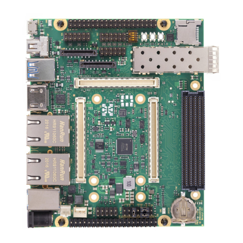
Enclustra Mars PM3-R5 User manual

Enclustra GmbH –Räffelstrasse 28 –CH- 8045 Zürich –Switzerland
Phone +41 43 343 39 43 –www.enclustra.com
Mars PM3-R5
User Manual
Project Info
Project Manager
Martin Heimlicher
Author(s)
Silvio Ziegler, Christoph Glattfelder
Reviewer(s)
Christoph Glattfelder
Version
1.09
Date
23/04/2019

23/04/2019 2 / 43 Version 1.09
Copyright reminder
Copyright © 2019 by Enclustra GmbH, Switzerland. All rights are reserved.
Unauthorized duplication of this document, in whole or in part, by any means is prohibited without the
prior written permission of Enclustra GmbH, Switzerland.
Although Enclustra GmbH believes that the information included in this publication is correct as of the
date of publication, Enclustra GmbH reserves the right to make changes at any time without notice.
All information in this document is strictly confidential and may only be published by Enclustra GmbH,
Switzerland.
All referenced trademarks are the property of their respective owners.
Document History
Version
Date
Author
Comment
1.00
30.04.2012
S. Ziegler
First release
1.01
01.06.2012
S. Ziegler
Updated ambient temperature specification
1.02
25.06.2012
S. Ziegler
Updated technical data section
1.03
04.07.2012
S. Ziegler
Updated errata for R2
1.04
09.07.2012
S. Ziegler
Added more detailed info about FX3 boot
mode options
1.05
03.08.2012
S. Ziegler
Added more details about Oscillator and boot
mode configuration options
1.06
26.05.2014
C. Glattfelder
Added SD-Card
1.07
1.12.2015
C. Glattfelder
Update for Revision 5
1.08
05.11.2018
D. Ungureanu
Corrected I2C expander signals description
and DIP switches description
1.09
23.04.2019
M. Moser
Updated section 1.3 with warning about
PM3/FMC AN1/Heat Sink collision

23/04/2019 3 / 43 Version 1.09
Table of Contents
1.1 General ..........................................................................................................................................5
1.1.1 Warranty........................................................................................................................................................................5
1.1.2 RoHS ...............................................................................................................................................................................5
1.1.3 Disposal and WEEE....................................................................................................................................................5
1.1.4 Safety Recommendations and Warnings.........................................................................................................6
1.1.5 Electro-Static Discharge..........................................................................................................................................6
1.1.6 EMC.................................................................................................................................................................................6
1.2 Deliverables ..................................................................................................................................6
1.3 Accessories....................................................................................................................................6
2.1 Block Diagram ..............................................................................................................................7
2.2 Features .........................................................................................................................................7
2.3 Part Numbers and Ordering Codes...........................................................................................8
2.4 Top View .......................................................................................................................................9
2.5 Bottom View...............................................................................................................................10
2.6 Dimensions .................................................................................................................................11
2.7 DIP Switches ...............................................................................................................................12
2.8 Connector Pinouts .....................................................................................................................13
2.8.1 J200 –Mars Module Connector........................................................................................................................13
2.8.2 J400 –USB 2.0 Micro-B Connector..................................................................................................................16
2.8.3 J500 –USB 3.0 B Connector ...............................................................................................................................17
2.8.4 J501 –USB 2.0 A Connector...............................................................................................................................17
2.8.5 J700 –RJ45 Ethernet.............................................................................................................................................. 17
2.8.6 J800 –FPGA JTAG Connector ............................................................................................................................17
2.8.7 J801 –FX3 Connector ...........................................................................................................................................18
2.8.8 J1000 –mini HDMI Connector ..........................................................................................................................19
2.8.9 J1100 –FMC LPC Connector ..............................................................................................................................19
2.8.10 J1101 –Extension Connector (Not Assembled) ......................................................................................... 23
2.8.11 J1200 –SD-Card......................................................................................................................................................23
2.8.12 J1300 –Power Connector....................................................................................................................................24
2.8.13 J1301 –Internal Power Connector...................................................................................................................24
2.8.14 J1302 –Fan Connector .........................................................................................................................................25
2.8.15 J1303 –Battery Holder .........................................................................................................................................25
2.9 Hardware description................................................................................................................25
2.9.1 Buttons........................................................................................................................................................................ 25
2.9.2 Flash Configuration Multiplexer .......................................................................................................................26
2.9.3 Fifo Mode Multiplexer ..........................................................................................................................................27
2.9.4 LEDs..............................................................................................................................................................................29
2.9.5 I2C IO Expander ....................................................................................................................................................... 29
2.9.6 RTC Battery................................................................................................................................................................ 30
2.9.7 I2C EEPROM...............................................................................................................................................................30

23/04/2019 4 / 43 Version 1.09
2.9.8 System Monitor.......................................................................................................................................................31
2.9.9 Cypress FX3 USB 3.0 Controller ........................................................................................................................31
2.9.10 USB 2.0 UART Device ............................................................................................................................................36
3.1 Absolute Maximum Ratings.....................................................................................................37
3.2 Recommended Operating Conditions ....................................................................................37
3.3 Mechanical data .........................................................................................................................38
4.1 Ordering ......................................................................................................................................39
4.2 Support........................................................................................................................................39
5.1 Differential pairs net lengths ...................................................................................................40

23/04/2019 5 / 43 Version 1.09
1Overview
This user manual only applies for Revision 5 boards and newer. These boards have two DIP switches. If
your Mars PM3 only has one DIP switch please get a previous version of this user manual from our
download page
1
.
1.1 General
The Mars PM3 Board is equipped with a multitude of I/O interfaces for the use with the Mars FPGA
and embedded processing module family. The board is equally well suited for rapid prototyping as
well as for building low-quantity FPGA systems without the need of developing custom hardware.
Furthermore, the board can be used for production flashing of Mars modules or for educational
purposes.
Benefits:
•Support for USB 3.0 device and USB 2.0 host
•High-Speed FPGA and flash programming over USB
•USB 3.0 to FPGA communication available in SPI, I2C and 16 or 32 Bit slave FIFO modes
•5 differential pairs per HDMI connector usable for various high-speed I/O applications
•I/O interfaces for almost all applications
•Industry-standard FMC low pin count connector
•Simple integration thanks to a single 12V supply voltage
•Alternatively, power can be supplied by the USB device port
1.1.1 Warranty
For information concerning the warranty please read through the “General Business Conditions” on
Enclustra’s website
2
.
1.1.2 RoHS
The Mars module are designed and produced according to the Restriction of Hazardous Substances
(RoHS) Directive (2011/65/EC).
1.1.3 Disposal and WEEE
The Mars modules must be disposed properly at the end of its life span. If a battery is installed onto
the board it must also be disposed correctly.
The Mars modules are not designed “ready for operation” for the end-user. The Waste Electrical and
Electronic Equipment (WEEE) Directive (2002/96/EC) is not applicable for the Mars boards. Nonetheless
users should still dispose the product properly at the end of life.

23/04/2019 6 / 43 Version 1.09
1.1.4 Safety Recommendations and Warnings
Ensure that the power supply is disconnected from the board before inserting or removing a Mars
module, connecting interfaces, replacing SD-Cards and batteries, connecting jumpers, etc.
Take special care with the mounting orientation of Mars modules –they can fit in the connectors both
ways round. The base board and the module may be damaged if inserted the wrong way and powered
up.
Touching the capacitors of the DC-DC converters can lead to voltage peaks and permanent damage.
Over-voltage on power or signal lines can cause permanent damage.
1.1.5 Electro-Static Discharge
Electronic boards are sensitive to Electro-Static Discharge (ESD). Please ensure that the product is
handled with care and only in an ESD protected environment.
1.1.6 EMC
This is a Class A product and is not intended to be used in domestic environments. The product may
cause electromagnetic interference in which appropriate measures must be taken.
1.2 Deliverables
•Mars PM3 Board
•Mars PM3 user manual (this document)
•Mars PM3 schematics1
•Mars PM3 IO Netlength sheet1
1.3 Accessories
•Mars MX1, MX2, AX3, ZX2, ZX3 or MA3 module
•12V Power Supply
•USB 3.0 A to B cable
•JTAG Adapter board for FX3 and FPGA debugging (JTAG-PM3)
Warning
Enclustra FMC AN1 board not usable when using Enclustra Mars heat sink:
If an Enclustra Mars heat sink is mounted on the inserted module, the FMC AN1
Board cannot be mounted since it collides with the heat sink and cannot be fit into
the FMC connector on the PM3 completely.

23/04/2019 7 / 43 Version 1.09
2Module Description
2.1 Block Diagram
Figure 1: Mars PM3 board overview
2.2 Features
•Mars 200-pin SO-DIMM connector
•FMC low pin count connector
•Gigabit Ethernet RJ45 connector
•HDMI connector for PCIe or LVDS applications
•USB 3.0 B connector (device)
•USB 2.0 A (host) and Micro-B (device) connectors
•Cypress FX3 USB 3.0 device controller
•USB 2.0 High-Speed UART controller
•General purpose I/O connectors, fan connector, 2 push buttons, 5 LEDs
•Battery holder for real time clock
•SD-Card holder, connected to user IOs on FPGAs and bootable MIO pins on the Mars ZX3
Warning
Do not insert other SO-DIMM modules except Mars Enclustra FPGA Modules!
FMC restrictions apply when using 32 Bit FX3 interface

23/04/2019 8 / 43 Version 1.09
2.3 Part Numbers and Ordering Codes
Every module has a label with a marking specifying the part number and the serial number, as shown
in Figure 2:
Figure 2: Module label
Table 1 shows the correspondence between part number and ordering code.
Part number
Ordering code
EN100581
MA-PM3-I-R3
EN100582
MA-PM3-C-R3
EN100745
MA-PM3-W-R4
EN100746
MA-PM3-C-R4
EN101233
MA-PM3-C-R5
EN101234
MA-PM3-W-R5
Table 1: Part Numbers and Ordering Codes
EN100000
SN123456
Part Number
Serial Number

23/04/2019 9 / 43 Version 1.09
2.4 Top View
Figure 3: Top view

23/04/2019 10 / 43 Version 1.09
2.5 Bottom View
Figure 4: Bottom view

23/04/2019 11 / 43 Version 1.09
2.6 Dimensions
J800 (FPGA JTAG), J801 (FX3 Connector) and J1101 (IO Connector) are 2.54 mm pin headers.
Figure 5: Dimensions

23/04/2019 12 / 43 Version 1.09
2.7 DIP Switches
The tables below show the functions of the configuration DIP switches. The options printed bold are
the default settings.
Switch
(CFG-A / S1200)
Off
On
1
Reserved (will be VCC_IO = 1.8V in
future versions)
VCC_IO is 2.5V or 3.3V
(depending on Switch 2)
2
VCC_IO is 2.5V
VCC_IO is 3.3V
3
USB from FPGA module routed to
USB 2.0 A connector (J501)
USB from FPGA module routed to
USB 3.0 B connector J500 (FX3
USB connection disabled)
4
Board powered from DC Power
Input (J1300)
Board powered from USB (J500) if
J1300 not connected
Table 2: DIP switch CFG-A settings
Switch
(CFG-B / S1204)
Off
On
1
Pull down on the BOOT_MODE
signal of the Mars module (Mars
connector pin 190, SPI flash boot
mode on most modules)
Pull up on the BOOT_MODE signal
of the Mars module
(passive serial or SD-Card boot
mode depending on the module)
2
Mars connector pin 170 floating
Mars connector pin 170 tied to
GND (used as BOOT_MODE1 on
some modules)
3
Mars connector pin 168 floating
Mars connector pin 168 tied to
GND
4
FTDI USB UART routed to pins
34+36 of the Mars connector
FTDI USB UART routed to pins
153+155 of the Mars connector
(for use with SOC modules, only
use if the FX3 FIFO interface is not
used)
Table 3: DIP switch CFG-B settings
Warning
If DIP Switch S1200-4 is on (board powered from USB) then the board must not be
powered from J1301 at the same time. Otherwise the Mars PM3 gets severely damaged.

23/04/2019 13 / 43 Version 1.09
2.8 Connector Pinouts
Table 4 shows an overview of all connectors assembled on the Mars PM3 Board. A more detailed
description of each connector can be found further below in this section.
Connector
Description
Connected to
J200
Mars Module Connector
Mars FPGA module
J400
USB 2.0 Micro-B Connector
USB 2.0 UART Device (U401)
J500
USB 3.0 B Connector
Cypress FX3 USB 3.0 controller (U301)
and Mars Module Connector
J501
USB 2.0 A Connector
Mars Module Connector
J700
RJ45 Ethernet Port (1G or 2x 100M)
Mars Module Connector
J800
FPGA JTAG Connector
Mars Module Connector
J801
FX3 Connector
Cypress FX3 USB 3.0 Controller (U301)
and System Monitor
J802
SD-Card holder (on bottom side)
Mars Module Connector (shared with
FX3 FIFO interface)
J1000
HDMI / PCIe Port
Mars Module Connector
J1100
FMC LPC Connector
Mars Module Connector
J1101
Extension Connector (not assembled)
Mars Module Connector
J1300
External Power Jack (12V DC,
2.1x5.5mm)
Power Supplies
J1301
Internal Power Connector
Power supplies
J1302
Fan Connector
System Monitor
J1303
Battery Holder (on bottom side)
Mars Module Connector (RTC)
Table 4: Connector overview
2.8.1 J200 –Mars Module Connector
2nd Function
Signal
Connector Pin
Signal
2nd Function
VCC_5V
1
2
GND
VCC_5V
3
4
FMC_CLK1_M2C_P
VCC_5V
5
6
FMC_CLK1_M2C_N
VCC_5V
7
8
GND

23/04/2019 14 / 43 Version 1.09
VCC_5V
9
10
PCIE_REFCLK_P
VCC_5V
11
12
PCIE_REFCLK_N
PGOOD_CARRIER
13
14
GND
GND
15
16
PCIE_PET1_P
PCIE_PER1_P
17
18
PCIE_PET1_N
PCIE_PER1_N
19
20
GND
GND
21
22
PCIE_PET0_P
PCIE_PER0_P
23
24
PCIE_PET0_N
PCIE_PER0_N
25
26
GND
GND
27
28
FMC_LA31_P
FMC_LA33_P
29
30
FMC_LA31_N
FMC_LA33_N
31
32
GND
GND
33
34
UART_TXD
FMC_LA32_P
35
36
UART_RXD
FMC_LA32_N
37
38
GND
GND
39
40
PWR_GOOD_MOD
VMON_P41
41
42
VMON_P42
FMC_LA17_CC_P
43
44
FMC_LA19_P
FMC_LA17_CC_N
45
46
FMC_LA19_N
GND
47
48
FMC_LA20_P
FMC_LA18_CC_P
49
50
FMC_LA20_N
FMC_LA18_CC_N
51
52
GND
VCC_IO
53
54
FMC_LA22_P
FMC_LA21_P
55
56
FMC_LA22_N
FMC_LA21_N
57
58
FMC_LA24_P
FMC_LA23_P
59
60
FMC_LA24_N
FMC_LA23_N
61
62
VCC_IO
GND
63
64
FMC_LA26_P
FMC_LA25_P
65
66
FMC_LA26_N
FMC_LA25_N
67
68
FMC_LA28_P
FMC_LA27_P
69
70
FMC_LA28_N
FMC_LA27_N
71
72
GND
VCC_IO
73
74
FMC_LA29_P
FMC_LA15_P
75
76
FMC_LA29_N
FMC_LA15_N
77
78
FMC_LA30_P

23/04/2019 15 / 43 Version 1.09
FMC_LA16_P
79
80
FMC_LA30_N
FMC_LA16_N
81
82
VCC_IO
GND
83
84
FMC_LA02_P
FMC_LA00_CC_P
85
86
FMC_LA02_N
FMC_LA00_CC_N
87
88
GND
VCC_OUT
89
90
FMC_LA03_P
FX3_DQ28
FMC_LA04_P
91
92
FMC_LA03_N
FX3_DQ29
FMC_LA04_N
93
94
VMON_P94
GND
95
96
FMC_LA05_P
FX3_DQ25
FX3_DQ24
FMC_LA06_P
97
98
FMC_LA05_N
FX3_DQ26
FX3_DQ27
FMC_LA06_N
99
100
GND
VCC_OUT
101
102
FMC_LA07_P
FX3_DQ31
FMC_LA01_CC_P
103
104
FMC_LA07_N
FX3_DQ30
FMC_LA01_CC_N
105
106
VMON_P106
GND
107
108
FMC_LA09_P
FX3_DQ18
FX3_DQ21
FMC_LA08_P
109
110
FMC_LA09_N
FX3_DQ16
FX3_DQ22
FMC_LA08_N
111
112
FMC_CLK0_M2C_P
FX3_DQ19
FMC_LA10_P
113
114
FMC_CLK0_M2C_N
FX3_DQ23
FMC_LA10_N
115
116
GND
VCC_IO
117
118
FMC_LA12_P
FX3_DQ20
FMC_LA11_P
119
120
FMC_LA12_N
FX3_DQ17
FMC_LA11_N
121
122
FMC_LA14_P
FMC_LA13_P
123
124
FMC_LA14_N
FMC_LA13_N
125
126
VCC_IO
GND
127
128
FX3_DQ13
USER_BTN#
FX3_FLAGB
129
130
FX3_DQ12
FX3_A1
131
132
FX3_DQ11
FX3_CLK
133
134
FX3_DQ14
FX3_FLAGA
135
136
GND
VCC_IO
137
138
FX3_DQ15
SD_CLK
FX3_SLRD#
139
140
FX3_DQ9
SD_CMD
FX3_SLWR#
141
142
FX3_DQ10
SD_D0
FX3_SLOE#
143
144
FX3_DQ8
SD_D1
FX3_PKTEND#
145
146
VCC_IO
GND
147
148
FX3_DQ7

23/04/2019 16 / 43 Version 1.09
SD_D2
FX3_DQ3
149
150
FX3_DQ4
SD_D3
3
FX3_DQ1
151
152
FX3_DQ6
SD-Card detect
UART_RX
FX3_DQ0
153
154
FX3_DQ5
UART_TX
FX3_DQ2
155
156
GND
GND
157
158
JTAG_TCK
USB_DP
159
160
JTAG_TDI
USB_DM
161
162
JTAG_TMS
USB_VBUS
163
164
JTAG_TDO
USB_ID
165
166
USB_CPEN
GND
167
168
RSVD_P168
ETH_A_N
169
170
RSVD_P170
BOOT_MODE1
ETH_A_P
171
172
GND
ETH0_LED1#
173
174
I2C_INT#
ETH0_LED2#
175
176
I2C_SDA
ETH_B_N
177
178
I2C_SCL
ETH_B_P
179
180
GND
ETH_CTREF
181
182
FLASH _CLK
ETH_C_N
183
184
FLASH_DO
ETH_C_P
185
186
FLASH_DI
ETH1_LED1#
187
188
FLASH_CS#
ETH1_LED2#
189
190
BOOT_MODE
ETH_D_N
191
192
SRST#_RDY#
ETH_D_P
193
194
FPGA_DONE
GND
195
196
POR#_LOAD#
VCC_3V3
197
198
VMON_P198
VCC_3V3
199
200
VBAT
Table 5: J200 –Mars module connector
2.8.2 J400 –USB 2.0 Micro-B Connector
The USB 2.0 Micro-B Connector J400 allows simple RS232 communication between a host computer
and the Mars PM3 board using the USB interface. The USB 2.0 UART device U401 can be accessed
from the host computer using a virtual COM port driver to display debug messages or sending control
commands to the Mars PM3 board. The UART device is connected to the Mars module and the FX3
controller; make sure that the RX line is only driven by one device!
Normally the USB UART is connected to pins 34 and 36 of the Mars connector like the previous
versions of the Mars PM3. If DIP switch 4 of CFG-B is set to ON the UART will be routed to pins 153

23/04/2019 17 / 43 Version 1.09
and 155 for use with SOC modules. Please note that these pins are shared with the FX3 FIFO interface
and must only be used as UART if the FX3 FIFO interface is not used!
Power and data signals on this connector are protected against ESD incidents.
2.8.3 J500 –USB 3.0 B Connector
This USB connector can be used in two modes:
a) S1200-3 is off: The Cypress FX3 USB 3.0 controller’s USB signals are routed to J500 and allow
300 MB/s high speed communication between the host computer and Mars PM3 Board.
b) S1200-3 is on: If the inserted Mars module features a USB controller, the USB signals of this
module are routed to J500 to allow device mode operation. In this mode only USB 1.1 and 2.0
are supported.
This connector has the power and data signals protected against ESD incidents.
2.8.4 J501 –USB 2.0 A Connector
If the inserted Mars module features a USB controller, the USB signals of this module are connected to
J501 and allow USB host mode operation. The power output on J501 can be switched on and off using
the signal USB_CPEN that controls a USB load switch U502. Power and data signals on this connector
are ESD protected.
2.8.5 J700 –RJ45 Ethernet
This connector can be operated in two modes:
a) If the inserted Mars module supports gigabit Ethernet, then this port provides one gigabit
Ethernet link.
b) If the inserted Mars module supports dual 100 MBit Ethernet, then this port provides two 100
MBit Ethernet links using an external adapter.
There is no need to set the Ethernet mode on the DIP switch as in previous versions anymore.
2.8.6 J800 –FPGA JTAG Connector
The FPGA JTAG connector allows accessing the JTAG port of the inserted FPGA module. The signals on
this connector are protected against ESD incidents.
For easier connection of the Xilinx and Altera JTAG programmers there is a breakout board with the
standard connectors available. This adapter is included in the hardware kits only. If you order a single
Mars PM3 please ask for a JTAG-PM3 if you need the adapter board.
Warning
The JTAG pins are connected to the FPGA with only small series impedance. Only apply
VCC_IO compliant voltages to the IO pins. Any other voltages may damage the FPGA
as well as other devices on the Mars PM3 Board or the installed Mars FPGA module.

23/04/2019 18 / 43 Version 1.09
Comment
Signal
Connector Pin
Signal
Comment
VCC_IO
1
2
VCC_IO
SRST#_RDY#
3
4
GND
FPGA_TDI
5
6
GND
FPGA_TMS
7
8
GND
FPGA_TCK
9
10
GND
GND
11
12
GND
FPGA_TDO
13
14
GND
Not Connected
15
16
GND
SVD_P168
17
18
GND
SVD_P170
19
20
GND
Table 6: J800 –FPGA JTAG connector
2.8.7 J801 –FX3 Connector
The main purpose of this connector is to access the JTAG port of the Cypress FX3 USB 3.0 controller. In
addition, this connector feeds out four GPIO pins of the FX3 that can be used if the slave FIFO interface
is not operated in 32 Bit mode. The SYSMON and VBAT signals are also accessible on this connector as
well as the FX3 reset signal that can be pulled down to reset the Cypress FX3 USB controller. All signals
on this connector are ESD protected.
Comment
Signal
Connector Pin
Signal
Comment
12V
VCC_MAIN
1
2
FX3_RESET_EXT#
GND
3
4
VCC_5V
VCC_3V3
5
6
BOOT_MODE
VBAT_IN
7
8
GND
SYSMON_GPI
9
10
SYSMON_GPO#
FX3_TRST#
11
12
FX3_GPIO0
FX3_TMS
13
14
FX3_GPIO1
FX3_TDO
15
16
FX3_GPIO2
FX3_TDI
17
18
FX3_GPIO3
FX3_TCK
19
20
GND
Table 7: J801 –FX3 connector
Warning
The IO pins are directly connected to the Cypress FX3 USB 3.0 controller or other
peripherals. Only apply VCC_IO compliant voltages to the IO pins. Any other voltages
may damage the FX3 as well as other devices on the Mars PM3 Board.

23/04/2019 19 / 43 Version 1.09
2.8.8 J1000 –mini HDMI Connector
The signals on J1000 are connected to Multi-Gigabit-Transceivers, if available on the FPGA module.
When using FPGA modules that do not support Gigabit-Transceivers, these signals can be used for
high speed differential IOs (e.g. LVDS). The signals are directly routed to the FPGA (no AC coupling)
with additional ESD protection. Some signals have alternative functions as indicated in the comments
row. VCC_5V_HDMI is provided on the connector as 5V 150mA supply voltage.
Comment
Signal
Connector Pin
Signal
Comment
GND
1
2
PCIE_PER1_P
PCIE_PER1_N
3
4
GND
PCIE_PET0_P
5
6
PCIE_PET0_N
GND
7
8
PCIE_PER0_P
PCIE_PER0_N
9
10
GND
PCIE_REFCLK_P
11
12
PCIE_REFCLK_N
GND
13
14
PCIE_WAKE#
22k pull-up
I2C_SCL, 10k pull-up
PCIE_PERST#
15
16
PCIE_PRSNT
I2C_SDA, 10k pull-up
PCIE_PET1_N
17
18
VCC_HDMI
5V 150mA
PCIE_PET1_P
19
-
-
Table 8: J1000 –mini HDMI connector
2.8.9 J1100 –FMC LPC Connector
This connector allows extending Mars PM3 boards with Enclustra (e.g. FMC DR2 Module) or third-party
160 pin LPC FMC modules.
Comment
Signal
Connector Pin
Signal
Comment
Not connected
H1
G1
GND
Not connected
H2
G2
FMC_CLK1_M2C_P
GND
H3
G3
FMC_CLK1_M2C_N
N
Warning
The IO pins are directly connected to the FPGA. Only apply VCC_IO compliant voltages
to the IO pins. Any other voltages may damage the FPGA as well as other devices on
the Mars PM3 Board or the installed Mars FPGA module.
Warning
The IO pins are directly connected to the FPGA. Only apply VCC_IO compliant voltages
to the IO pins. Any other voltages may damage the FPGA as well as other devices on
the Mars PM3 Board or the installed Mars FPGA module.

23/04/2019 20 / 43 Version 1.09
FMC_CLK0_M2C_P
H4
G4
GND
FMC_CLK0_M2C_N
H5
G5
GND
GND
H6
G6
FMC_LA00_CC_P
FMC_LA02_P
H7
G7
FMC_LA00_CC_N
FMC_LA02_N
H8
G8
GND
GND
H9
G9
FMC_LA03_P
FX3_DQ28
FMC_LA04_P
H10
G10
FMC_LA03_N
FX3_DQ29
FMC_LA04_N
H11
G11
GND
GND
H12
G12
FMC_LA08_P
FX3_DQ21
FMC_LA07_P
H13
G13
FMC_LA08_N
FX3_DQ22
FMC_LA07_N
H14
G14
GND
GND
H15
G15
FMC_LA12_P
FX3_DQ20
FMC_LA11_P
H16
G16
FMC_LA12_N
FX3_DQ17
FMC_LA11_N
H17
G17
GND
GND
H18
G18
FMC_LA16_P
FMC_LA15_P
H19
G19
FMC_LA16_N
FMC_LA15_N
H20
G20
GND
GND
H21
G21
FMC_LA20_P
FMC_LA19_P
H22
G22
FMC_LA20_N
FMC_LA19_N
H23
G23
GND
GND
H24
G24
FMC_LA22_P
FMC_LA21_P
H25
G25
FMC_LA22_N
FMC_LA21_N
H26
G26
GND
GND
H27
G27
FMC_LA25_P
FMC_LA24_P
H28
G28
FMC_LA25_N
FMC_LA24_N
H29
G29
GND
GND
H30
G30
FMC_LA29_P
FMC_LA28_P
H31
G31
FMC_LA29_N
FMC_LA28_N
H32
G32
GND
GND
H33
G33
FMC_LA31_P
FMC_LA30_P
H34
G34
FMC_LA31_N
FMC_LA30_N
H35
G35
GND
GND
H36
G36
FMC_LA33_P
FMC_LA32_P
H37
G37
FMC_LA33_N
FMC_LA32_N
H38
G38
GND
This manual suits for next models
6
Table of contents
Other Enclustra Motherboard manuals
