EnOcean STM 300 User manual

USER MANUAL V1.26
EnOcean GmbH
Kolpingring 18a
82041 Oberhaching
Germany
Phone +49.89.67 34 689-0
Fax +49.89.67 34 689-50
info@enocean.com
www.enocean.com
Subject to modifications
STM 300 / STM 300C User Manual V1.26
February 25, 2011 11:18 AM
Page 1/1
Patent protected:
WO98/36395, DE 100 25 561, DE 101 50 128,
WO 2004/051591, DE 103 01 678 A1, DE 10309334,
WO 04/109236, WO 05/096482, WO 02/095707,
US 6,747,573, US 7,019,241
Observe precautions! Electrostatic sensitive devices!
Scavenger Transceiver Module
STM 300 / STM 300C
February 25, 2011

USER MANUAL V1.26
© 2010 EnOcean | www.enocean.com STM 300 / STM 300C User Manual V1.26 | Page 2/2
STM 300 / STM 300C
REVISION HISTORY
The following major modifications and improvements have been made to the first version of
this document:
No Major Changes
1.01 Tape running direction added in 3.8
1.10 Application note for multiple digital inputs with WAKE functionality added.
1.20 Error corrected in 3.5.1. and 4.1: Maximum gain of external antenna at 50 Ohm
output RF_50 is 0 dBi!
1.25 Charging circuit in 3.1 corrected; remarks added regarding use of IOVDD in 2.3.
Parameters of A/D converter corrected and specified in more detail in 2.3.2
1.26 Optional resolution at ADIO0, ADIO1, ADIO2 corrected in 2.3. Detailed description
in 2.9.1 was correct!
Published by EnOcean GmbH, Kolpingring 18a, 82041 Oberhaching, Germany
www.enocean.com, info@enocean.com, phone ++49 (89) 6734 6890
© EnOcean GmbH
All Rights Reserved
Important!
This information describes the type of component and shall not be considered as assured characteris-
tics. No responsibility is assumed for possible omissions or inaccuracies. Circuitry and specifications
are subject to change without notice. For the latest product specifications, refer to the EnOcean web-
site: http://www.enocean.com.
As far as patents or other rights of third parties are concerned, liability is only assumed for modules,
not for the described applications, processes and circuits.
EnOcean does not assume responsibility for use of modules described and limits its liability to the
replacement of modules determined to be defective due to workmanship. Devices or systems contain-
ing RF components must meet the essential requirements of the local legal authorities.
The modules must not be used in any relation with equipment that supports, directly or indirectly,
human health or life or with applications that can result in danger for people, animals or real value.
Components of the modules are considered and should be disposed of as hazardous waste. Local
government regulations are to be observed.
Packing: Please use the recycling operators known to you.

USER MANUAL V1.26
© 2010 EnOcean | www.enocean.com STM 300 / STM 300C User Manual V1.26 | Page 3/3
STM 300 / STM 300C
TABLE OF CONTENT
1GENERAL DESCRIPTION .................................................................................4
1.1 Basic functionality..........................................................................................4
1.2 Technical data ...............................................................................................5
1.3 Physical dimensions .......................................................................................5
1.4 Environmental conditions................................................................................6
1.5 Ordering Information .....................................................................................6
2FUNCTIONAL DESCRIPTION ............................................................................7
2.1 Simplified firmware flow chart and block diagram ..............................................7
2.2 Hardware pin out...........................................................................................8
2.3 Pin description and operational characteristics...................................................9
2.3.1 GPIO supply voltage.................................................................................10
2.3.2 Analog and digital inputs ..........................................................................12
2.4 Absolute maximum ratings (non operating) ....................................................13
2.5 Maximum ratings (operating) ........................................................................13
2.6 Power management and voltage regulators.....................................................13
2.7 Charge control output (CCO).........................................................................14
2.8 Configuration ..............................................................................................15
2.8.1 Configuration via pins...............................................................................15
2.8.2 Configuration via programming interface ....................................................16
2.9 Radio telegram............................................................................................17
2.9.1 Normal operation.....................................................................................17
2.9.2 Teach-in telegram....................................................................................18
2.10 Transmit timing ......................................................................................18
2.11 Energy consumption................................................................................19
3APPLICATIONS INFORMATION.......................................................................20
3.1 How to connect an energy harvester and energy storage ..................................20
3.2 Using the SCO pin........................................................................................21
3.3 Using the WAKE pins....................................................................................22
3.4 Using RVDD ................................................................................................23
3.5 Antenna options ..........................................................................................24
3.5.1 Overview ................................................................................................24
3.5.2 Whip antenna..........................................................................................25
3.5.3 Chip antenna...........................................................................................26
3.5.4 Splatch antenna ......................................................................................28
3.5.5 Helical antenna........................................................................................29
3.6 Layout recommendations for foot pattern .......................................................30
3.7 Soldering information...................................................................................33
3.8 Tape & Reel specification ..............................................................................34
3.9 Transmission range......................................................................................35
4AGENCY CERTIFICATIONS ............................................................................36
4.1 CE Approval ................................................................................................36
4.2 FCC (United States) certification ....................................................................37
4.3 IC (Industry Canada) certification ..................................................................40
USER MANUAL V1.26
© 2010 EnOcean | www.enocean.com STM 300 / STM 300C User Manual V1.26 | Page 4/4
STM 300 / STM 300C
1GENERAL DESCRIPTION
1.1 Basic functionality
The extremely power saving RF transmitter
module STM 300 of EnOcean enables the
realization of wireless and maintenance free
sensors and actuators such as room operat-
ing panels, motion sensors or valve actua-
tors for heating control.
Power supply is provided by an external en-
ergy harvester, e.g. a small solar cell (e.g.
EnOcean ECS 3x0) or a thermal harvester.
An energy storage device can be connected
externally to bridge periods with no supply
from the energy harvester. A voltage limiter avoids damaging of the module when the sup-
ply from the energy harvester gets too high. The module provides a user configurable cyclic
wake up. After wake up a radio telegram (input data, unique 32 bit sensor ID, checksum)
will be transmitted in case of a change of any digital input value compared to the last send-
ing or in case of a significant change of measured analogue values (different input sensitivi-
ties can be selected). In case of no relevant input change a redundant retransmission signal
is sent after a user configurable number of wake-ups to announce all current values. In
addition a wake up can be triggered externally.
Features with built-in firmware
3 A/D converter inputs
4 digital inputs
Configurable wake-up and transmission cycle
Wake-up via Wake pins
Voltage limiter
Threshold detector
Application notes for calculation of energy budgets and management of external energy
storages
Product variants
STM 300/300C: SMD mountable module for use with external antenna (868/315 MHz)
Features accessible via API
Using the Dolphin API library it is possible to write custom firmware for the module.
STM 300 / STM 300C is in-system programmable. The API provides:
Integrated 16 MHz 8051 CPU with 32 KB FLASH and 2 kB SRAM
Receiver functionality
Various power down and sleep modes down to typ. 0.2 µA current consumption
Up to 16 configurable I/Os
10 bit ADC, 8 bit DAC

USER MANUAL V1.26
© 2010 EnOcean | www.enocean.com STM 300 / STM 300C User Manual V1.26 | Page 5/5
STM 300 / STM 300C
1.2 Technical data
A
ntenna External whip or 50 antenna mountable
Fre
q
uenc
y
315.0 MHz (STM 300C)/868.3 MHz (STM 300)
Radio Standard EnOcean 868 MHz/315 MHz
Data rate/Modulation t
yp
e 125 kbps/ASK
Receiver Sensitivity (at 25 °C) receiver available only via API, typ. –96 dBm1(868MHz)
typ. -98 dBm1(315MHz)
Conducted Out
p
ut Power typ. 5 dBm
Power Su
pp
l
y
2.1 V–4.5 V, 2.6 V needed for start-up
Current Consum
p
tion Deep Sleep mode : typ. 0.2 µA
Transmit mode: typ. 24 mA, max. 33 mA
Receive mode (available via API only): typ. 33 mA, max. 43 mA
In
p
ut Channels 4x digital input, 2x WAKE input , 3x analog input
Resolution: 3x 8 bit or 1x 10 bit, 1x 8 bit, 1x 6 bit
Radio Re
g
ulations R&TTE EN 300 220 (STM 300)
FCC CFR-47 Part 15 (STM 300C)
1.3 Physical dimensions
STM 300 / STM 300C (pads on bottom side of PCB!)
1@ 0.1% telegram error rate (based on 3 transmitted sub-telegrams)
PCB dimensions STM 300/STM 300C: 22x19x3.1 mm
Weight 1.9 g
Unless otherwise specified dimensions are in mm.
Tolerances:
PCB outline dimensions ±0.2 mm
All other tolerances ±0.1 mm
USER MANUAL V1.26
© 2010 EnOcean | www.enocean.com STM 300 / STM 300C User Manual V1.26 | Page 6/6
STM 300 / STM 300C
1.4 Environmental conditions
Operating temperature -25 °C … +85 °C
Storage temperature -40 °C … +85 °C
Storage temperature in tape & reel package -20 °C … +50 °C
Humidity 0% … 93% r.h., non-condensing
1.5 Ordering Information
Type Ordering Code Frequency
STM 300 S3001-D300 868.3 MHz
STM 300C S3031-D300 315.0 MHz
Suited solar cells (for technical details please refer to the ECS3x0 data sheet):
Type Ordering Code Size
ECS 300 S3005-D305 35.0×12.8×1.1 mm
ECS 310 S3005-D310 50.0×20.0×1.1 mm

USER MANUAL V1.26
© 2010 EnOcean | www.enocean.com STM 300 / STM 300C User Manual V1.26 | Page 7/7
STM 300 / STM 300C
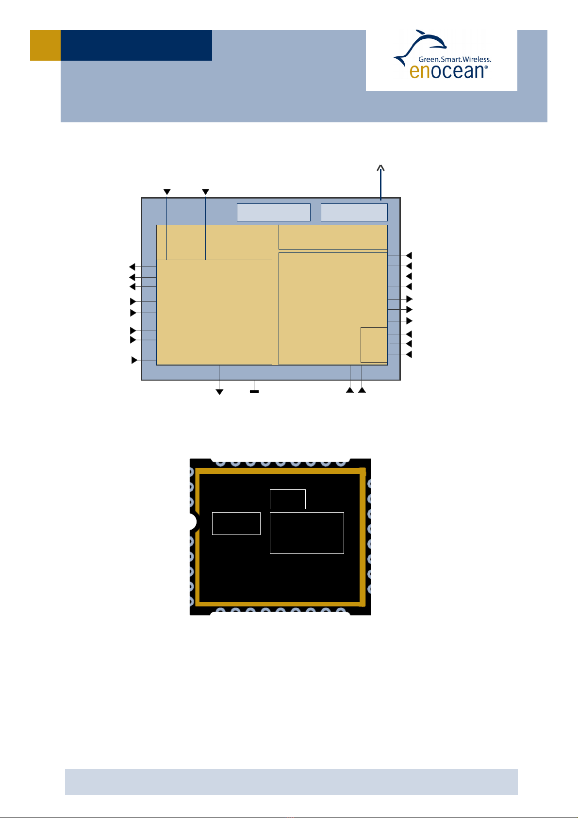
2FUNCTIONAL DESCRIPTION
2.1 Simplified firmware flow chart and block diagram
USER MANUAL V1.26
© 2010 EnOcean | www.enocean.com STM 300 / STM 300C User Manual V1.26 | Page 8/8
STM 300 / STM 300C
2.2 Hardware pin out
The figure above shows the pin out of the STM 300 hardware. The pins are named accord-
ing to the naming of the EO3000I chip to simplify usage of the DOLPHIN API.
The table in section 2.3 shows the translation of hardware pins to a naming that fits the
functionality of the built-in firmware. When writing own firmware based on the DOLPHIN
API please refer to the Dolphin Core Description and use this manual only for information
regarding the module hardware, such as pin out, layout recommendations, charging cir-
cuitry, antenna options, and approvals.
V_OUT
AD_2
AD_1
AD_0
DI_3
DI_2
DI_1
DI_0
GNDGND
CW_1
CW_0
WAKE0
CP_1CP_0
LED
LRN
VDD RF_50
RF_WHIP
VDDLIM
UVDD
IOVDD
RESET
CCO
BALUN
Presence Signal
(every 100th,
every 10th,
every cyclic wake-up
or SW defined)
Spontaneous
wake-up
Cyclic Wake-up
(every 1s ,10s , 100s,
or SW defined)
A/D
Digital
Inputs
Power management Micro
Controller
RF Transceiver
868.3 MHz (STM300)
315.0 MHz (STM300C)
DOLPHIN
EO3000I
16MHz Oscillator
DVDD
SCO
EO3000I
Antenna
balun
XTAL
16MHz
STM300 – TOP VIEW
DVDD
IOVDD
SCSEDIO0
PROG_EN
SCLKDIO1
WSDADIO2
RSDADIO3
GND
UVDD
WXIDIO
WXODIO
WAKE1
RESET
WAKE0
GND
GND
GND
ADIO0
ADIO1
ADIO2
ADIO3
ADIO4
ADIO5
ADIO6
ADIO7
GND
RVDD
GND
GND
RF_50
RF_WHIP
VDDLIM
VDD
GND
1
9
18
26

USER MANUAL V1.26
© 2010 EnOcean | www.enocean.com STM 300 / STM 300C User Manual V1.26 | Page 9/9
STM 300 / STM 300C
2.3 Pin description and operational characteristics
STM 300
Hardware
Symbol
STM 300
Firmware
Symbol
Function Characteristics
GND GND Ground connection Must be connected to GND
VDD VDD Supply voltage 2.1 V – 4.5 V; Start-up voltage: 2.6 V
Maximum ripple: see 2.6
RVDD
V_OUT
RF supply voltage
regulator output
1.8 V. Output current: max. 10 mA.
See 3.4!
Supply for external circuitry, available
while not in deep sleep mode.
DVDD
DVDD
Digital supply volt-
age regulator out-
put
1.8 V. Output current: max. 5 mA
Supply for external circuitry, available
while not in deep sleep mode.
UVDD
UVDD
Ultra low power
supply voltage
regulator output
Not for supply of external circuitry!
For use with WAKE pins, see section 3.3.
Max. 1 µA output current!
VDDLIM
VDDLIM
Supply voltage
limiter input
Limitation voltage: 4.5 V
Maximum shunting current: 50 mA
IOVDD
IOVDD
GPIO supply volt-
age
Must be connected to desired interface
supply voltage as specified in 2.5, e.g. to
DVDD. See also 2.3.1
RESET
RESET
Reset input
Programming I/F
Active high reset (1.8 V)
Connect external 10 kpull-down.
PROG_EN
PROG_EN
Programming I/F HIGH: programming mode active
LOW: operating mode
Digital input, connect external 10 kpull-
down.
ADIO0
AD_0
Analog input Input read ~2 ms after wake-up.
Resolution 8 bit (default) or 10 bit.
See also 2.3.2.
ADIO1 AD_1 Analog input Input read ~2 ms after wake-up.
Resolution 8 bit (default) or 6 bit.
See also 2.3.2.
ADIO2 AD_2 Analog input Input read ~2 ms after wake-up.
Resolution 8 bit.
See also 2.3.2.
ADIO3 DI_0 Digital input Input read ~2 ms after wake-up.
See also 2.3.2.
ADIO4
DI_1
Digital input Input read ~2 ms after wake-up.
See also 2.3.2.
ADIO5 DI_2 Digital input Input read ~2 ms after wake-up.
See also 2.3.2.
ADIO6 DI_3 Digital input Input read ~2 ms after wake-up.
See also 2.3.2.
ADIO7 LED Transmission
indicator LED
Max. output current:
2 mA @ IOVDD=3.3 V
0.65 mA @ IOVDD=1.8 V

USER MANUAL V1.26
© 2010 EnOcean | www.enocean.com STM 300 / STM 300C User Manual V1.26 | Page 10/10
STM 300 / STM 300C
Programming I/F
SCSEDIO0 CW_1
Encoding input for
wake-up cycle
Leave open or connect to GND
Programming I/F
SCLKDIO1
CW_0 Encoding input for
wake-up cycle
Leave open or connect to GND
Programming I/F
WSDADIO2
CP_1 Encoding input for
retransmission
Leave open or connect to GND
Programming I/F
RSDADIO3
CP_0 Encoding input for
retransmission
Leave open or connect to GND
Programming I/F
WXIDIO SCO Sensor control Digital output, max. current 15 µA
HIGH ~x ms before analog inputs are read
(x=0…508 ms; default 2 ms.)
LOW at wake-up and after reading of
analog inputs
Polarity can be inverted, delay time can be
programmed, see 2.8.2.
WXODIO CCO Charge control Max output current 15 µA
See 2.7 for description of behaviour.
WAKE0 WAKE0 Wake input Change of logic state leads to wake-up and
transmission of a telegram. See also 3.3.
WAKE1 LRN LRN input Change of logic state to LOW leads to
wake-up and transmission of teach-in tele-
gram if a manufacturer code is pro-
grammed. See also 2.9.2 and 3.3.
RF_WHIP RF_WHIP RF output Output for whip antenna
RF_50 RF_50 RF output 50 Ohm output for external antenna
2.3.1 GPIO supply voltage
For digital communication with other circuitry (peripherals) the digital I/O configured pins
of the mixed signal sensor interface (ADIO0 to ADIO7) and the pins of the programming
interface (SCSEDIO0, SCLKDIO1, WSDADIO2, RSDADIO3) may be operated from supply
voltages different from DVDD. Therefore an interface supply voltage pin IOVDD is available
which can be connected either to DVDD or to an external supply within the tolerated volt-

USER MANUAL V1.26
© 2010 EnOcean | www.enocean.com STM 300 / STM 300C User Manual V1.26 | Page 11/11
STM 300 / STM 300C
age range of IOVDD. Please note that the wristwatch XTAL I/Os WXIDIO and WXODIO are
always supplied from UVDD.
If DVDD=0 V (e.g. in any sleepmode) and IOVDD is supplied, there may be un-
predictable and varyin
g
current from IOVDD caused by internal floatin
g
nodes. It
must be taken care that the current into IOVDD does not exceed 10 mA while
DVDD=0 V.
If DVDD=0 V and IOVDD is not supplied, do not apply voltage to any above men-
tioned pin. This may lead to unpredictable malfunction of the device.
IOVDD voltage must not exceed VDD voltage! A malfunction of the module may be
caused by such inverse supply!
For I/O pins configured as analog pins the IOVDD voltage level is not relevant!
However it is important to connect IOVDD to a supply voltage as specified in 2.5.
USER MANUAL V1.26
© 2010 EnOcean | www.enocean.com STM 300 / STM 300C User Manual V1.26 | Page 12/12
STM 300 / STM 300C
10
0x00
0xFF
ideal
real
Offset Error
Gain Error
CodeADC
UADC
URVDD
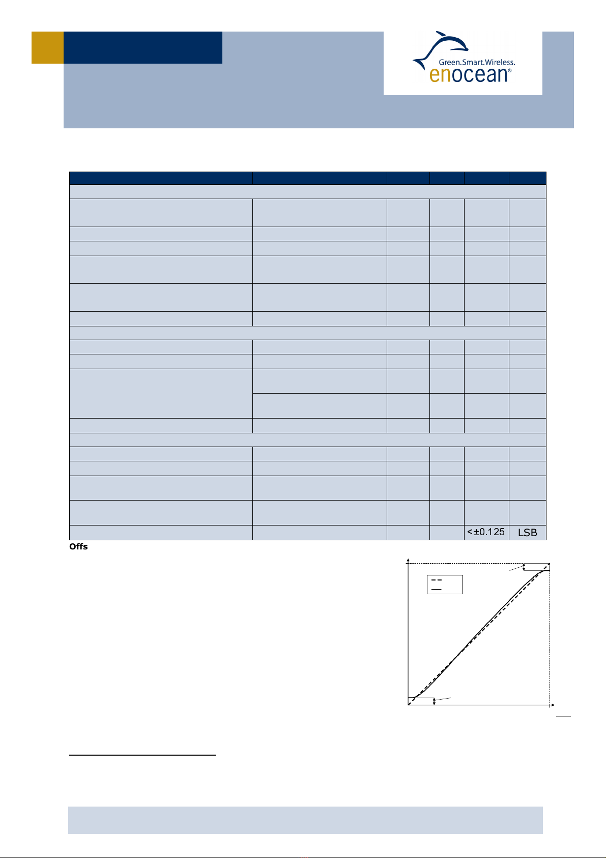
2.3.2 Analog and digital inputs
Parameter Conditions / Notes Min Typ Max Units
Analog Input Mode
Measurement range Single ended
Internal reference RVDD/2
0.067 RVDD-
0.12
V
Input coupling DC
Measurement bandwidth262.5 kHz
Input impedance Single ended against
GND @ 1 kHz
10 MΩ
Input capacitance Single ended against
GND @ 1 kHz
10 pF
Effective measurement resolution 10 Bit
10bit measurement
Offset error 23 36 LSB
Gain error 32 62 LSB
INL
Code <=200 +3
-14
+6
-23
LSB
Code >200 +3
-4
+6
-10
LSB
DNL <±0.5 LSB
8bit measurement
Offset error 6 9 LSB
Gain error 8 16 LSB
INL Code <=50 +1
-4
+2
-6
LSB
Code >50 +1
-1
+2
-3
LSB
DNL
<±0.125
LSB
Offset Error: Describes the offset between the minimal possible code and
code 0x00.
Gain Error: Describes the offset between maximum possible code and full
scale (e.g. 0x3FF for 10bit measurements).
Integral Non-Linearity (INL): Describes the difference between the ideal
characteristics and the real characteristics. Only values between minimum and
maximum possible code are considered (excluding offset error and gain error).
Differential Non-Linearity (DNL): Measures the maximum deviation from
the ideal step size of 1 LSB (least significant bit).
Effective resolution: Results from the signal-noise ratio of the ADC and is
given in Bit. The number describes how many bits can be measured stable. The
criterion selected here is that the noise of DNL is <±0.5 LSB.
Measurement Bandwidth: The measurement bandwitdh is internally limited
by filters. A quasi static signal must be applied as long as the filter needs to
settle. SettlingTime= 1/(MeasurementBandwidth)*ln(2^resolution[Bit])
For further details please refer to the Dolphin Core Description.
23dB input bandwidth, resulting in 111µs settling time to achieve a deviation of an input
signal <1LSB (<0.098% @ 10bit resolution).

USER MANUAL V1.26
© 2010 EnOcean | www.enocean.com STM 300 / STM 300C User Manual V1.26 | Page 13/13
STM 300 / STM 300C
Parameter Conditions / Notes Min Typ Max Units
Digital Input Mode
Input HIGH voltage 2/3
IOVDD
V
Input LOW voltage 1/3
IOVDD
V
Pull up resistor @IOVDD=1.7 … 1.9 V 90 132 200 kΩ
@IOVDD=3.0 … 3.6 V 38 54 85 kΩ
2.4 Absolute maximum ratings (non operating)
Symbol Parameter Min Max Units
VDD
VDDLIM Supply voltage at VDD and VDDLIM -0.5 5.5 V
IOVDD GPIO supply voltage -0.5 3.6 V
GND Ground connection 0 0 V
VINA Voltage at every analog input pin -0.5 2 V
VIND1 Voltage at RESET, WAKE0/1, and every digital input
pin except WXIDIO/WXODIO
-0.5 3.6 V
VIND2 Voltage at WXIDIO / WXODIO input pin -0.5 2 V
2.5 Maximum ratings (operating)
Symbol Parameter Min Max Units
VDD
VDDLIM Supply voltage at VDD and VDDLIM VOFF 4.5 V
IOVDD GPIO supply voltage (see also 2.3.1)
1.7 MIN
(3.6;
VDD)
V
GND Ground connection 0 0 V
VINA Voltage at every analog input pin 0 2.0 V
VIND1 Voltage at RESET, WAKE0/1, and every digital input
pin except WXIDIO / WXODIO
0 3.6 V
VIND2 Voltage at WXIDIO / WXODIO input pin 0 2.0 V
2.6 Power management and voltage regulators
Symbol Parameter Conditions / Notes Min Typ Max Units
Voltage Regulators
VDDR Ripple on VDD, where
Min(VDD) > VON
50 mVpp
UVDD Ultra Low Power supply 1.8 V
RVDD RF supply 1.7 1.8 1.9 V
DVDD Digital supply 1.7 1.8 1.9 V

USER MANUAL V1.26
© 2010 EnOcean | www.enocean.com STM 300 / STM 300C User Manual V1.26 | Page 14/14
STM 300 / STM 300C
Voltage Limiter
VLIM Limitation voltage 4.5 V
ILIM Shunting current 50 mA
Threshold Detector
VON Turn on threshold 2.3 2.45 2.6 V
VOFF Turn off threshold Automatic shutdown if
VDD drops below VOFF
1.85 1.9 2.1 V
Voltage Limiter
STM 300 provides a voltage limiter which limits the supply voltage VDD of STM 300 to a
value VDDLIM which is slightly below the maximum VDD ratings by shunting of sufficient
current.
Threshold detector
STM 300 provides an ultra low power ON/OFF threshold detector. If VDD > VON, it turns on
the ultra low power regulator (UVDD), the watchdog timer and the WAKE# pins circuitry. If
VDD VOFF it initiates the automatic shut down of STM 300.
2.7 Charge control output (CCO)
After startup STM 300 provides the output signal of the threshold detector at CCO.
CCO is supplied by UVDD. The output value remains stable also when STM 300 is in deep
sleep mode.
Behavior of CCO
-At power up: TRISTATE until VDD>VON then HIGH
-if VDD>VON then HIGH
-if VDD<VON then LOW
-if VDD< VOFF then LOW or TRISTATE
For definition of VON and VOFF please refer to 2.6.
VDD
t
TRISTATE
VOFF
VON
VDD > VON VDD < VON
VDD < VOFF
TRISTATE
or LOW
CCO
VDD
1.8V
0V
~0.9V
VDD
t
TRISTATE
VOFF
VON
VDD > VON VDD < VON
VDD < VOFF
TRISTATE
or LOW
CCO
VDD
1.8V
0V
~0.9V

USER MANUAL V1.26
© 2010 EnOcean | www.enocean.com STM 300 / STM 300C User Manual V1.26 | Page 15/15
STM 300 / STM 300C
2.8 Configuration
2.8.1 Configuration via pins
The encoding input pins have to be left open or connected to GND in correspondence with
the following connection schemes. These settings are checked at every wake-up.
Wake-up cycle time
CW_0 CW_1 Wake-up cycle time
NC NC 1 s ±20%
GND NC 10 s ±20%
NC GND 100 s ±20%
GND GND No cyclic wake-up
Redundant retransmission
Via CP_0 and CP_1 an internal counter is set which is decreased at every wake-up signal.
Once the counter reaches zero the redundant retransmission signal is sent.
CP_0 CP_1 Number of wake-ups that
trigger a redundant retransmission
NC NC Every timer wake-up signal
GND NC Every 7th - 14th timer wake-up signal, affected at random
NC GND Every 70th - 140th timer wake-up signal, affected at random
GND GND No redundant retransmission
A radio telegram is always transmitted after wake-up via WAKE pins!
After transmission the counter is reset to a random value within the specified in-
terval.
According to FCC 15.231a) a redundant retransmission at every timer wake-up to
determine the system integrity is only allowed in safety and security applications!
In this case the total transmission time must not exceed two seconds per hour,
which means that a combination with a 1 s wake-up cycle time is not allowed!
If applied in other (non-safety, non-security) applications a minimum of 10 s be-
tween periodic transmissions is required. In addition the device has to comply with
the lower field strength limits of 15.231e). The limited modular approval of STM
300C is not valid in this case.

USER MANUAL V1.26
© 2010 EnOcean | www.enocean.com STM 300 / STM 300C User Manual V1.26 | Page 16/16
STM 300 / STM 300C
2.8.2 Configuration via programming interface
Via the programming interface the configuration area can be modified. This provides a lot
more configuration options. Values set via programming interface override hardware set-
tings! These settings are read after RESET or power-on reset only and not at every wake-
up of the module!
The interface is shown in the figure below:
EnOcean provides EOPx (EnOcean Programmer, a command line program) and Dolphin
Studio (Windows application for chip configuration, programming, and testing) and the
USB/SPI programmer device as part of the EDK 300 developer´s kit.
Parameter Configuration
via pins
Configuration
via programming interface
Wake up cycle See section 2.8.1 Value can be set from 1 s to 65534 s
Redundant
Retransmission cycle
See section 2.8.1 Min…Max values for random interval
If Min=Max -> random switched off
Threshold values for
analog inputs
No The default values are: 5 LSB at AD_1 input, 6
LSB at AD_0 and 14 LSB at AD_2.
The threshold value can be set between 0 and
full scale for every input individually.
Resolution of the analog
inputs
No Default: AD_0: 8 bit, AD_1: 8 bit, AD_2: 8 bit
Option: AD_0: 10 bit, AD_1: 6 bit, AD_2: 8 bit
Input mask No A digital input mask for ignoring changes on
digital input pins. At default all input bits are
checked.
Delay time between SCO on
and sampling moment
No Value can be set from 0 ms to 508 ms in steps
of 2 ms. Default delay time is 2 ms.
Source of AD_2 No Select if AD_2 contains measurement value of
external ADIO2 pin or from internal VDD/4
Polarity of SCO signal No Polarity can be inversed.
Edge of wake pin change
causing a telegram trans-
mission
No Every change of a wake pin triggers a wake-up.
For both wake pins it can be configured indi-
vidually if a telegram shall be sent on rising,
falling or both edges.
Manufacturer ID and EEP
(EnOcean Equipment Profile)
No Information about manufacturer and type of
device. This feature is needed for “automatic”
interoperability of sensors and actuators or bus
systems. Information how to set these parame-
ters requires an agreement with EnOcean.
Unique manufacturer IDs are distributed by the
EnOcean Alliance.
USB <=> SPI
interface SPI
USB
Dolphin Studio, or EOP
Reset
PROG_EN
ADIO7
SCSEDIO0
SCLKDIO1
WSDADIO2
RSDADIO3
STM
300
USER MANUAL V1.26
© 2010 EnOcean | www.enocean.com STM 300 / STM 300C User Manual V1.26 | Page 17/17
STM 300 / STM 300C
2.9 Radio telegram
2.9.1 Normal operation
Telegram content (seen at programming interface of RCM 130/TCM 3x0 or at DOLPHIN
API):
ORG = 0x07 (Telegram type “4BS”)
Data_Byte1..3
3x8bit mode:
DATA_BYTE3 = Value of AD_2 analog input
DATA_BYTE2 = Value of AD_1 analog input
DATA_BYTE1 = Value of AD_0 analog input
1x8bit, 1x6it, 1x10bit mode:
DATA_BYTE3 = Value of AD_2
DATA_BYTE2 = Upper 2 bits of AD_0 and value of AD_1
DATA_BYTE1 = Lower 8 bits Value of AD_0 analog input
DATA_BYTE0 = Digital sensor inputs as follows:
Bit 7 Bit 0
Reserved, set to 0 DI_3 DI_2 DI_1 DI_0
ID_BYTE3 = module identifier (Byte3)
ID_BYTE2 = module identifier (Byte2)
ID_BYTE1 = module identifier (Byte1)
ID_BYTE0 = module identifier (Byte0)
DATA_BYTE3 DATA_BYTE2 DATA_BYTE1
AD_2 AD_1 AD_0
7 6 5 4 3 2 1 0 5 4 3 2 1 0 9 8 7 6 5 4 3 2 1 0
The voltages measured at the analog inputs can be calculated from these values as follows:
U=(Value of AD_x)/(2n)x1.8 V n=resolution of channel in bit
USER MANUAL V1.26
© 2010 EnOcean | www.enocean.com STM 300 / STM 300C User Manual V1.26 | Page 18/18
STM 300 / STM 300C
2.9.2 Teach-in telegram
In case a manufacturer code is programmed into the module the module transmits – in-
stead of transmitting a normal telegram – a dedicated teach-in telegram if
digital input DI_3=0 at wake-up or
wake-up via WAKE1 pin (LRN input)
With this special teach-in telegram it is possible to identify the manufacturer of a device
and the function and type of a device. There is a list available from the EnOcean Alliance
describing the functionalities of the respective products.
If no manufacturer code is programmed the module does not react to signal
changes on WAKE1 (LRN input)!
ORG = 0x07 (Telegram type “4BS”)
DATA_BYTE0..3 see below
LRN Type = 1
LRN = 0
DI0..DI2: current status of digital inputs
Profile, Type, Manufacturer-ID defined by manufacturer
RE0..2: set to 0
ID_BYTE3 = module identifier (Byte3)
ID_BYTE2 = module identifier (Byte2)
ID_BYTE1 = module identifier (Byte1)
ID_BYTE0 = module identifier (Byte0)
ORG Data_Byte3 Data_Byte2 Data_Byte1 Data_Byte0 ID
Function
6 Bit
Type
7 Bit
Manufacture
r
-
ID 11 Bit
LRN Type
1Bit
RE2
1Bit
RE1
1Bit
RE0
1Bit
LRN
1Bit
DI2
1Bit
DI1
1Bit
DI0
1Bit
2.10 Transmit timing
The setup of the transmission timing allows avoiding possible collisions with data packages
of other EnOcean transmitters as well as disturbances from the environment. With each
transmission cycle, 3 identical subtelegrams are transmitted within 40 ms. The transmis-
sion of a subtelegram lasts approximately 1.2 ms. The delay between the three transmis-
sion bursts is affected at random.
If a new wake-up occurs before all sub-tele
g
rams have been sent, the series of
transmissions is stopped and a new series of telegrams with new valid measure-
ment values is transmitted.

USER MANUAL V1.26
© 2010 EnOcean | www.enocean.com STM 300 / STM 300C User Manual V1.26 | Page 19/19
STM 300 / STM 300C
2.11 Energy consumption
Current Consumption of STM 300
Charge needed for one measurement and transmit cycle: ~130 µC
Charge needed for one measurement cycle without transmit: ~30 µC
(current for external sensor circuits not included)
Calculations are performed on the basis of electric charges because of the internal linear
voltage regulator of the module. Energy consumption varies with voltage of the energy
storage while consumption of electric charge is constant.
From these values the following performance parameters have been calculated:
Wake
cycle
[s]
Transmit
interval
Operation Time
in darkness [h]
when storage
fully charged
Required reload
time [h] at 200
lux within 24 h
for continuous
operation
24 h operation
after 6 h
illumination
at x lux
Illumina-
tion level
in lux for
continuous
operation
Current
in µA
required
for con-
tinuous
operation
1 1 0.5 storage too small storage too small
5220 130.5
1 10 1.7 storage too small storage too small
1620 40.5
1 100 2.1 storage too small storage too small
1250 31.3
10 1 5.1 storage too small storage too small
540 13.5
10 10 16 21 storage too small
175 4.4
10 100 20 16.8 storage too small
140 3.5
100 1 43 7.8 260 65 1.6
100 10 98 3.6 120 30 0.8
100 100 112 3 100 25 0.6
Assumptions:
Storage PAS614L-VL3 with 0.25 F, Umax=3.2 V, Umin=2.2 V, T=25°C
Consumption: Transmit cycle 100 µC, measurement cycle 30 µC
Indoor solar cell, operating values 3 V and 5 µA @ 200 lux fluorescent light
(e.g. ECS 300 solar cell)
Current proportional to illumination level (not true at very low levels!)
These values are calculated values, the accuracy is about +/-20%!
0.00001
0.0001
0.001
0.01
0.1
1
10
100
0 102030405060708090100
Time [ms]
Current [mA]
USER MANUAL V1.26
© 2010 EnOcean | www.enocean.com STM 300 / STM 300C User Manual V1.26 | Page 20/20
STM 300 / STM 300C
3APPLICATIONS INFORMATION
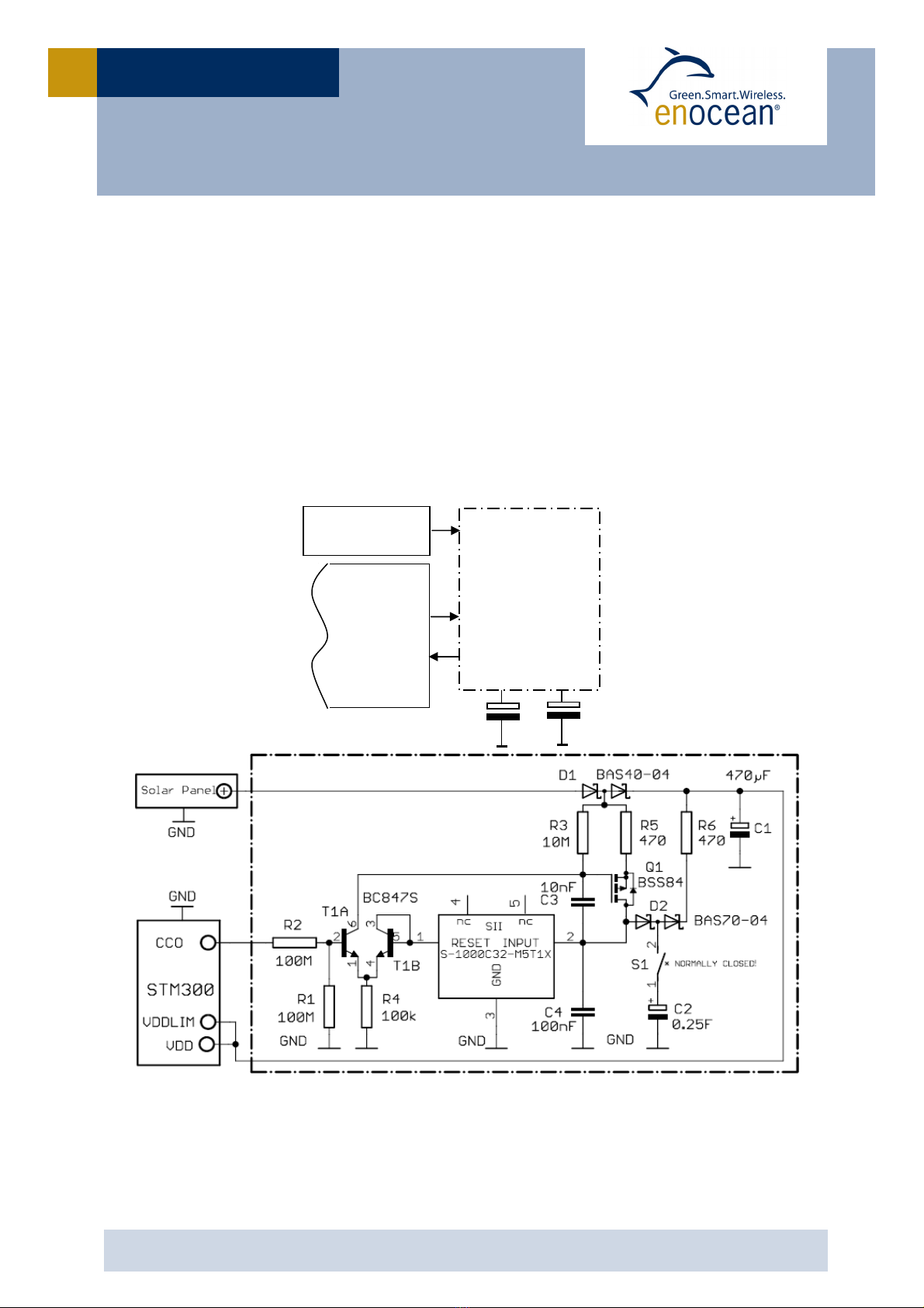
3.1 How to connect an energy harvester and energy storage
STM 300 is designed for use with an external energy harvester and energy storage.
In order to support a fast start-up and long term operation with no energy supply available
usually two different storages are used. The small storage fills quickly and allows a fast
start-up. The large storage fills slowly but once it is filled up it provides a large buffer for
times where no energy is available, e.g. at night in a solar powered sensor.
STM 300 provides a digital output CCO (see also 2.7) which allows controlling the charging
of these two storages. At the beginning, as long as the voltage is below the VON voltage
only the small storage is filled. Once the threshold is reached the CCO signal changes and
the large storage is filled. The short term storage capacitor (C1) is usually in the range of
470 to 1000 µF. For the long term storage we suggest a capacitor (C2) with a capacity of
0.25 F. Below an overview and the schematics of a charging circuitry is shown:
This circuit is designed for an energy storage capacitor specified up to 3.3 V (e.g. PAS614L-
VL3. Please pay great attention to manufacturers handling and soldering procedures!)
The S-1000C32-M5T1x voltage detector from SEIKO (SII) limits the voltage at C2 < 3.3 V,
to avoid damaging of the energy storage. In case a different voltage limit is required for C2
this component has to be exchanged by a suited variant.
STM 300
CCO
VDDLIM
VDD
Charge
Management
Long Short
te
rm term
storage storage
C2 C1
Solar Panel
(e.g. ECS 3x0)
Other manuals for STM 300
1
This manual suits for next models
1
Table of contents
Other EnOcean Transceiver manuals


