Epson S5U1C33001H1400 User manual

MANUAL
S5U1C33001H1400
S1C33 Family In-Circuit Debugger

Evaluation board/kit and Development tool important notice
1. This evaluation board/kit or development tool is designed for use for engineering evaluation, demonstration,
or development purposes only. Do not use it for other purpose. It is not intended to meet the requirement of
design for finished product.
2. This evaluation board/kit or development tool is intended for use by an electronics engineer, and it is not the
product for consumer. The user should use this goods properly and safely. Seiko Epson dose not assume any
responsibility and liability of any kind of damage and/or fire coursed by usage of it. User should cease to use
it when any abnormal issue occurs even during proper and safe use.
3. The part used for this evaluation board/kit or development tool is changed without any notice.
NOTICE
No part of this material may be reproduced or duplicated in any form or by any means without the written
permission of Seiko Epson. Seiko Epson reserves the right to make changes to this material without notice.
Seiko Epson does not assume any liability of any kind arising out of any inaccuracies contained in this material
or due to its application or use in any product or circuit and, further, there is no representation that this material is
applicable to products requiring high level reliability, such as, medical products. Moreover, no license to any
intellectual property rights is granted by implication or otherwise, and there is no representation or warranty that
anything made in accordance with this material will be free from any patent or copyright infringement of a third
party. When exporting the products or technology described in this material, you should comply with the
applicable export control laws and regulations and follow the procedures required by such laws and regulations.
You are requested not to use, to resell, to export and/or to otherwise dispose of the products (and any technical
information furnished, if any) for the development and/or manufacture of weapon of mass destruction or for other
military purposes.
All brands or product names mentioned herein are trademarks and/or registered trademarks of their respective
companies.
©SEIKO EPSON CORPORATION 2012,All rights reserved.

S1C33 Family In-Circuit Debugger EPSON i
S5U1C33001H1400 Manual (Rev. 0.20)
Table of Contents
1. GLOSSARY........................................................................................................................................ 1
2. OVERVIEW......................................................................................................................................... 2
2.1 Features...................................................................................................................................... 3
2.2 Operating environment ............................................................................................................... 6
3. COMPONENTS INCLUDED WITH PACKAGE .................................................................................. 7
4. NAME AND FUNCTION OF EACH PART.......................................................................................... 9
4.1 Left-side panel ............................................................................................................................ 9
4.1.1 10-pin connector for connecting to target systems ............................................................ 9
4.1.2 30-pin connector (not provided) for connecting to target systems ..................................... 9
4.1.3 4-pin connector for flash programmer power supply ......................................................... 9
4.1.4 Regarding the monitor pins ............................................................................................. 10
4.2 Right-side panel........................................................................................................................ 12
4.2.1 DIP switch ....................................................................................................................... 12
4.2.2 RESET/START switch ..................................................................................................... 14
4.2.3 USB connector ................................................................................................................ 14
4.3 Top panel .................................................................................................................................. 15
5. CONNECTION.................................................................................................................................. 18
5.1 Connecting the S5U1C33001H1400 and the host computer .................................................... 18
5.1.1 Connecting the USB Cable.............................................................................................. 18
5.1.2 USB Driver Installation Procedure................................................................................... 18
5.2 Connecting the target system ................................................................................................... 20
5.3 Connector for flash programmer power supply ......................................................................... 22
5.3.1 Target system reset signal output (TARGETRST OUT).................................................. 22
5.3.2 Target voltage input (TARGET VCC IN)........................................................................... 22
5.3.3 Flash programming voltage output (FLASH VCC OUT) .................................................. 23
6. START-UP METHOD (POWER-ON SEQUENCE) ........................................................................... 24
7. ICD MODE........................................................................................................................................ 26
7.1 ICD mode setting ...................................................................................................................... 26

ii EPSON S1C33 Family In-Circuit Debugger
S5U1C33001H1400 Manual (Rev. 0.20)
7.2 Invoking ICD mode ................................................................................................................... 26
7.3 Debugger start-up..................................................................................................................... 27
7.4 Connection test......................................................................................................................... 27
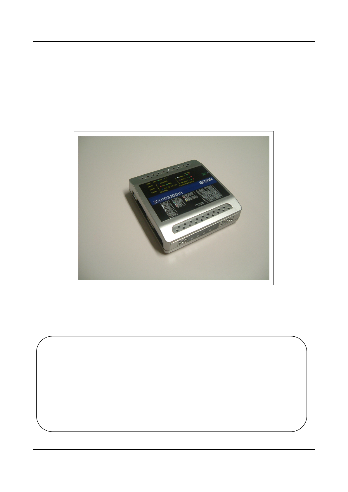
8. FLASH PROGRAMMER MODE ...................................................................................................... 28
8.1 Preparing for flash programming .............................................................................................. 28
8.2 Flash programmer mode operating method.............................................................................. 29
9. FIRMWARE UPDATE PROCEDURE ............................................................................................... 31
10. PRECAUTIONS.............................................................................................................................. 32
10.1 Restrictions on debugging ........................................................................................................ 32
10.1.1 Operation of the internal peripheral circuits ..................................................................... 32
10.1.2 Interrupts when the target program is not running........................................................... 32
10.1.3 Interrupts when the target program is executed in a single step ..................................... 32
10.1.4 Break functions................................................................................................................ 32
10.1.5 Trace function..................................................................................................................33
10.1.6 Counts of the execution counter...................................................................................... 33
10.1.7 Reserved areas in the internal peripheral circuits (C33 STD/Mini core) .......................... 34
10.1.8 Operating clock of the S5U1C33001H (C33 STD/Mini core) ........................................... 34
10.1.9 Area 2 of S1C33xxx (C33 STD/Mini/ADV core)............................................................... 34
10.1.10 Concurrent use of the S5U1C330M2S debug monitor .................................................... 34
10.1.11 Reset sequence .............................................................................................................. 35
10.1.12 Break functions when a reset request isaccepted .......................................................... 35
10.1.13 I/O memory dump by the S5U1C33001H........................................................................ 35
10.1.14 Parameter file ..................................................................................................................35
10.1.15 Models with cache memory embedded ........................................................................... 36
10.1.16 Models with MMU embedded .......................................................................................... 36
10.2 Differences from the actual IC ..................................................................................................37
10.2.1 Register initialization ....................................................................................................... 37
10.3 Usage precautions.................................................................................................................... 38
10.3.1 Connecting and disconnecting equipment....................................................................... 38
10.3.2 Powering on/off ............................................................................................................... 38
10.3.3 Connecting the target system.......................................................................................... 38

S1C33 Family In-Circuit Debugger EPSON iii
S5U1C33001H1400 Manual (Rev. 0.20)
10.3.4 Operation of the S5U1C33001H system ......................................................................... 38
10.3.5 Wiring between the S1C33xxx chip and target connector ............................................... 39
10.3.6 Reset request .................................................................................................................. 39
10.3.7 Notes on target system power supply.............................................................................. 39
10.3.8 Notes on S5U1C33001H power supply........................................................................... 40
10.3.9 Core Sync Simple Logic Analyzer Function..................................................................... 40
10.4 Implementation of the PC trace function ................................................................................... 41
10.5 Implementation of the bus trace function .................................................................................. 41
11. TROUBLESHOOTING.................................................................................................................... 42
12. SPECIFICATIONS .......................................................................................................................... 43

1. GLOSSARY
S1C33 Family In-Circuit Debugger EPSON 1
S5U1C33001H1400 Manual (Rev. 0.20)
1. GLOSSARY
S5U1C33001H1400 (ICD33V6.0)
ICD mode Flash programmer mode
This mode is used to debug the target system. Debugging
requires both a PC and the debugger (gdb. exe included in
the S5U1C33001C: C Compiler Package for S1C33
Family).
This mode is used to write programs to the target
system without a PC. Before writing a program to the
target system, you must load the program to the
S5U1C33001H1400 (ICD33V6.0) in ICD mode.
Debugger, gdb.exe (included in the S5U1C33001C: C Compiler Package for S1C33 Family)
Simulator (SIM) mode ICD6 mode
This mode simulates the execution of the target program on
a PC memory. This mode does not require any other tool.
However, this mode cannot execute ICD-dependent
functions.
This mode performs debugging using the
S5U1C33001H1400 (ICD33V6.0) or ICD board. The
program is executed on the target board. To debug
these products, use this debugger in ICD6 mode.
Target (S1C33xxx)
Normal mode Debug mode
Ordinary mode in which the target system executes a user
program.
The mode changes to debug mode under the following
conditions:
•When the break condition set by the debugger (gdb.exe)
is met
•When the user presses the Break button on the gdb
screen while the debugger (gdb.exe) is connected
•When a Low level is input to the target system DSIO pin
•When the CPU executes a brk command
In this mode, the target system accepts control by the
debugger (gdb.exe).
This mode permits various debugging operations,
including display and rewriting of data in registers and
memory.
This mode is activated when the S5U1C33001H1400
(ICD33V6.0) is connected and the power-on sequence
is executed.

2. OVERVIEW
2 EPSON S1C33 Family In-Circuit Debugger
S5U1C33001H1400 Manual (Rev. 0.20)
2. OVERVIEW
The S5U1C33001H1400 (In-Circuit Debugger for the S1C33 Family) is a hardware tool (emulator) that
allows software to be efficiently developed for the S1C33 Family of 32-bit Single-Chip Microcomputers. It
provides a software development environment by communicating with the S1C33xxx chip.
This manual primarily explains how to use the S5U1C33001H1400. For details on the debugger (gdb.exe)
functions and commands, refer to the “Debugger” section in the “S5U1C33001C Manual (C Compiler
Package for S1C33 Family)”. The figure below shows an external view of the S5U1C33001H.
Fig. 1 S5U1C33001H1400 external view
Note: Do not open the case as it may cause a malfunction.
Precautions before using the S5U1C33001H1400
Please read the sections shown below before getting started with the S5U1C33001H1400. These sections,
especially (2) and (3), describe the answers to frequently asked questions.
(1) “Components Included with Package”
Make sure all of the listed items are included with your package.
(2) “Connecting the S5U1C33001H and the host computer”
Install the USB driver before the S5U1C33001H can be used.
(3) “Connecting the target system”
Please pay particular attention to the Notes.

2. OVERVIEW
S1C33 Family In-Circuit Debugger EPSON 3
S5U1C33001H1400 Manual (Rev. 0.20)
2.1 Features
•C33 cores supported C33 STD core
C33 Mini core
C33 PE core
C33 ADV core
•Interface with the host PC USB 1.1
•Maximum data download speed About 65KB/s (Approx. 50 KB/s at 20 MHz)*1
•Mode supported by debugger ICD6 mode
•Program break function PC break function
Data break function
Forced break function
External forced break function (BRK IN)
Area break function
Bus break function
(logical or physical address is selectable)
Elapsed-time break function
•Trace function Normal PC trace function / normal bus trace
function
→(1 Mclk after a go command or 1 Mclk before a
break command can be traced)
→(Allows selection of logical or physical address
for bus trace)
Area PC trace function / area bus trace function
→Trace of area between trace trigger 1 and trace
trigger 2 only
→1 Mclk can be traced
→Allows selection of logical or physical address
for bus trace
Bus break trigger trace function
TRC IN pin input signal trace function
User logic signal trace function
•Measurement of the target program execution time
Measurement range of 3 us to 6515 hours
•Single-unit flash programmer function Provided
•Firmware update function Provided
•Clock frequency for communications with target system
4 kHz to 120 MHz

2. OVERVIEW
4 EPSON S1C33 Family In-Circuit Debugger
S5U1C33001H1400 Manual (Rev. 0.20)
•Power supply for flash programmer Provided (fixed at 7.0 V)
•Reset signal output to target system Provided
•Supported system I/O voltage 3.3 V, 1.8 V, input voltage (1.0 to 5.0 V) from target
system
•Connector for target system connection 4-pin, 10-pin, 30-pin *2
•Connector for flash programmer power supply 4-pin
*1 Frequency when I/O voltage = 3.3 V. The upper-limit frequency may be lower than the
specification value in certain cases, depending on ambient noise, temperature conditions,
product variations, etc.
*2 The product package does not include a 30-pin cable connector. Please contact us if you need
this cable connector.

2. OVERVIEW
S1C33 Family In-Circuit Debugger EPSON 5
S5U1C33001H1400 Manual (Rev. 0.20)
Table 1 ICD models and differences
S5U1C33001H
Model
Function S5U1C33000H Ver. 3.0 Ver. 4.0 Ver. 4.1 Ver. 6.0
C33 cores supported C33 STD core
C33 Mini core
C33 STD core
C33 Mini core
C33 PE core *5
C33 STD core
C33 Mini core
C33 PE core
C33 ADV core
C33 STD core
C33 Mini core
C33 PE core
C33 ADV core
Interface with the host PC Serial and
parallel I/F
USB 1.1 USB 1.1 USB 1.1
Data download speed
(maximum rate: DCLK = 40 MHz)
Serial I/F:
Approx. 8KB/s
Parallel I/F:
Approx. 30KB/s
About 65KB/s
(About 50KB/s
at 20 MHz)
About 65KB/s
(About 50KB/s at
20 MHz) *1
About 65KB/s
(About 50KB/s at
20 MHz) *1
Clock frequency to communicate with
the target
1 MHz to 40
MHz
1 MHz to 40
MHz
1 MHz to 40 MHz
*3
4 MHz to 40 MHz
Core clock frequency for using the
trace function
1 MHz to 60
MHz (3.3 V) *1
(10-pin cable)
1 MHz to 60
MHz (3.3 V)
(10-pin cable)
1 MHz to 120 MHz
(3.3 V)
*2, *3 (10-pin
cable, or 30-pin
coaxial cable)
4 MHz to 120 MHz
(3.3 V)
*2, *3, *6 (10-pin
cable, or 30-pin
coaxial cable)
Maximum trace capacity 128K clock
cycles
1M clock cycles 1M clock cycles 1M clock cycles
Single-unit flash programmer
function
- Available Available Available
Firmware update function - - Available Available
Mode supported by debugger ICD2 mode ICD3 mode ICD3 mode ICD6 mode
Bus trace function - - Available Available *6
Bus break trigger trace function - - Available Available *6
TRC IN pin input signal trace
function
- - Available Available
User logic signal trace function *4 - - Available Available
Target reset signal output - - Available Available
Target system I/O interface voltage 3.3 V 3.3 V 3.3 V and 1.8 V 3.3 V and 1.8 V, or
input voltage (1.0 to
5.0 V) from target
system
RESET/START switch - Available Available Available
DIP switch 4 bits 8 bits 8 bits 10 bits
LEDs for flash programmer - Available Available Available
Target system interface connector 10 pins 10 pins 10 pins, 30 pins 10 pins, 30 pins *6
Target system interface method 4 pins, 10 pins 4 pins, 10 pins 4 pins, 10 pins,
30 pins
4 pins, 10 pins, 30
pins *6
Target power supply connector - - 6 pins -
Connector for flash programmer
power supply
- - - 4 pins
*1 Indicates the frequency range for 3.3-V I/O. The upper-limit frequency may be lowered by environment noise,
temperature condition, S1C33 model, unevenness in quality, etc.
Note: In the model with the C33 STD or Mini core embedded, the maximum CPU core clock frequency is 60 MHz but
the maximum BCU (bus) clock frequency is 40 MHz. When operating the CPU with a clock higher than 40 MHz, the
BCU clock must be setup to 1/2 CPU core clock (#X2SPD = 0).
*2 The maximum frequency may be half or less of the described value when the I/O voltage is 1.8 V.

2. OVERVIEW
6 EPSON S1C33 Family In-Circuit Debugger
S5U1C33001H1400 Manual (Rev. 0.20)
*3 Supports 32 kHz by firmware update.
*4 Available only when the S1C33 model that supports the user logic signal trace function is used.
*5 Supports by firmware update.
*6 The product does not include a 30-pin cable for connecting to target systems or a connector for this cable. Please
contact us if you need a 30-pin cable.
Table 2 Correspondence between C33 cores and debug functions
Core
Function C33 STDMini C33 PE C33 ADV
DCLK while the program is halted = Bus clock = Core clock x set value = Core clock x set value
DCLK while the program is being
executed
= Core clock = Core clock = Core clock
PC trace method Level 1 Level 1 Level 2
Switching the DCLK-core clock
ratio
(DCLK while the program is
halted)
- {{
Address setup for the debug unit - {-
Area break function - - {
Bus break function - - {
Bus break trigger trace function - - {
TRC IN pin input signal trace
function
- - {
User logic signal trace function *7 - - {
Use of MMU in debug mode - - {
*7 Available only in S1C33 models that support the user logic signal trace function.
Except for the PC trace, Level 2 is upwardly compatible with Level 1 and realizes higher analytical accuracy than Level 1.
Functions not listed in the above table can be used regardless of the core model.
2.2 Operating environment
As the host computer, the S5U1C33001H1400 uses a PC with a USB port (USB 1.1) available.
Windows 2000 or Windows XP is recommended for the OS.

3. COMPONENTS INCLUDED WITH PACKAGE
S1C33 Family In-Circuit Debugger EPSON 7
S5U1C33001H1400 Manual (Rev. 0.20)
3. COMPONENTS INCLUDED WITH PACKAGE
The following shows the components included with the package:
(1) S5U1C33001H1400 (main unit) .................................................................................................................1
(2) USB cable (mini B).....................................................................................................................................1
(3) Target system interface cable (10-4 pin).....................................................................................................1
(4) Target system interface cable (10-10 pin)...................................................................................................1
(5) Target system power supply cable (4-4 pin) ...............................................................................................1
(6) Target system interface connectors (10-pin)...............................................................................................1
(7) Target system interface connectors (4-pin).................................................................................................1
(8) Target system power supply connectors (4-pin) ......................................................................................... 1
(9) User registration card ............................................................................................ English/Japanese, 1 each
(10) Warranty card........................................................................................................ English/Japanese, 1 each
(11) Usage precautions ................................................................................................. English/Japanese, 1 each
(12) Manual download guide........................................................................................ English/Japanese, 1 each
The items specified below are not included with the package. These items must be prepared separately.
(13) S5U1C33001H1400 User Manual (ICD33V6.0)
(PDF is downloadable from this PDF document and the SEIKO EPSON HP)
(14) Debugger (gdb.exe) for the S1C33 Family (included in the S1C33 Family C Compiler Package)
(15) Debugger manual for the S1C33 Family (included in the S1C33 Family C Compiler Package)

3. COMPONENTS INCLUDED WITH PACKAGE
8 EPSON S1C33 Family In-Circuit Debugger
S5U1C33001H1400 Manual (Rev. 0.20)
Fig. 2 Package components

4. NAME AND FUNCTION OF EACH PART
S1C33 Family In-Circuit Debugger EPSON 9
S5U1C33001H1400 Manual (Rev. 0.20)
4. NAME AND FUNCTION OF EACH PART
The following shows an external view of the S5U1C33001H1400’s operating section and the name of each part.
4.1 Left-side panel
Fig. 3 Left-side panel
4.1.1 10-pin connector for connecting to target systems
This connector is used to connect to the target system using a 10-pin cable or 10-pin-4-pin cable.
4.1.2 30-pin connector (not provided) for connecting to target systems
This connector is used to connect to the target system using a 30-pin cable.
Note: This connector is not provided with the debugger unit. Please contact us if you need
this cable.
Note: Only one of the 10-pin connector for connecting to target systems and 30-pin
connector for connecting to target systems may be used at any given time.
4.1.3 4-pin connector for flash programmer power supply
This connector is used to output a reset signal to the target system or to supply power
(note) for flash programming. When the interface for debug signals requires a voltage level
for the target system, this connector is used to input the operating voltage from the target
system. For information on the connector pin configuration and connection method, refer
to “Connector for flash programmer power supply.”
Note: The S5U1C1700H incorporates a 7-V, 200-mA power supply for flash programming.
However, use of this power supply may not be possible with certain S1C processors.
If the technical manual for the target S1C processor does not specifically mention
this power supply, damage may occur in the chip due to overvoltage. To prevent this
problem, avoid using this voltage (do not set the DIP SW8 to ON) if this voltage is
not supported by the target S1C processor. Keep this pin open when implementing a
connection terminal on the target board.

4. NAME AND FUNCTION OF EACH PART
10 EPSON S1C33 Family In-Circuit Debugger
S5U1C33001H1400 Manual (Rev. 0.20)
4.1.4 Regarding the monitor pins
•GND pin (black (left side in the above diagram))
To monitor the signals output from the above pins, connect the GND of a measuring
instrument such as an oscilloscope to this pin. If the ground level between the
S5U1C33001H and the target system is unstable (particularly when the 4-pin cable is
used), this pin can be used to stabilize the ground level.
•BRK IN pin (red)
If a low-level signal is input to this pin when the target program is being executed, the
target program execution is suspended. After a low level is input to the BRK IN
terminal, a break will occur after a few instructions have been executed.
•TRC IN pin (white)
This pin inputs an external trace signal. The input signal can also be traced when the
bus trace is performed.
•TRG OUT pin (light blue)
The TRG OUT pin outputs trace trigger signals indicating the start and end of the trace.
To perform an area trace with the S5U1C33001H, set two trigger points: the start
address and end address of the trace area. When the execution address of the program
corresponds to the set trace trigger point, the TRG OUT pin outputs a High-level signal.
It also outputs a High-level signal when target program execution is suspended. For a
discussion of how to set the trace function, see the “Debugger” section in the
S5U1C33001C Manual (C Compiler Package for S1C33 Family). The output timing is
shown below. To generate trace trigger signals, you must run the program for trace
trigger point 1 and point 2, in that order. Shown below are states in which trace triggers
are and are not generated.

4. NAME AND FUNCTION OF EACH PART
S1C33 Family In-Circuit Debugger EPSON 11
S5U1C33001H1400 Manual (Rev. 0.20)
Fig. 4 Examples of TRG OUT output timing
•EMUOUT pin (green)
This pin outputs a low level when the EMU/ERASE LED is lit (that is, when the
program is being executed) and outputs the 5 V level when that LCD is off (during a
break). This signal can be used as the protect signal for the S5U1C33xxxM emulation
memory.
•TRCFULL pin (blue (right side in the above diagram))
This is the trace full state output pin. This pin outputs a high level when the trace
memory becomes full.

4. NAME AND FUNCTION OF EACH PART
12 EPSON S1C33 Family In-Circuit Debugger
S5U1C33001H1400 Manual (Rev. 0.20)
4.2 Right-side panel
Fig. 5 Right-side panel
4.2.1 DIP switch
Note: After operating the DIP switches, press the RESET/START switch to apply the
settings.
•Selecting target CPU core (SW1)
Table 3-1 DIP SW1 setting
SW1 Setting
OPEN C33
ON C17 (Not supported)
•Selecting ICD mode/flash programmer mode (SW2, SW3)
Table 3-2 DIP SW2 and SW3 settings
SW2 SW3 Setting
OPEN OPEN ICD mode
ON OPEN Flash programmer mode Erase →Write
OPEN ON Flash programmer mode Verify
ON ON Flash mode Erase →Write →Verify
ICD mode: Mode for executing the debug command from the debugger in a PC (see the relevant section)
Flash programmer mode: Mode for operating the S5U1C33001H independently as a flash programmer (see relevant section)

4. NAME AND FUNCTION OF EACH PART
S1C33 Family In-Circuit Debugger EPSON 13
S5U1C33001H1400 Manual (Rev. 0.20)
•Selecting DSIO signal (SW4, SW5)
Table 3-3 DIP SW4 and SW5 settings
SW4 SW5 Setting
OPEN OPEN 3.3 V (default)
OPEN ON 1.8 V
ON OPEN Target system input voltage (1.0 to 5.0 V)
ON ON Target system input voltage (1.0 to 5.0 V)
Target system operating voltage applied to Pin No. 4 of the connector for flash programmer power supply.
•Selecting connection test (SW6)
Table 3-4 DIP SW6 setting
SW6 Setting
OPEN Connection test disabled (default)
ON Connection test enabled
Connection test: A communication check test is performed at the time of debugger invocation.
•Selecting firmware update mode (SW7)
Table 3-5 DIP SW7 setting
SW7 Setting
OPEN Off (default)
ON On
Turning this DIP switch ON enables connections between the S5U1C33001H and debugger without a target system. For
a discussion of how to update the firmware, refer to “Firmware Update.”
•Selecting flash programming voltage output (SW8)
Table 3-6 DIP SW8 setting
SW8 Setting
OPEN Off
ON On
Note: The S5U1C1700H incorporates a 7-V, 200-mA power supply for flash programming. However, use of this power
supply may not be possible with certain S1C processors. If the technical manual for the target S1C processor
does not specifically mention this power supply, damage may occur in the chip due to overvoltage. To prevent this
problem, avoid using this voltage (do not set the DIP SW8 to ON) if this voltage is not supported by the target S1C
processor.

4. NAME AND FUNCTION OF EACH PART
14 EPSON S1C33 Family In-Circuit Debugger
S5U1C33001H1400 Manual (Rev. 0.20)
•Selecting trace (SW9)
Table 3-7 DIP SW9 setting
SW9 Setting
OPEN Trace disabled
ON Trace enabled
•Option setting (SW10)
Table 3-8 DIP SW10 setting
SW10 Setting
OPEN Unused
ON Unused
4.2.2 RESET/START switch
< In ICD mode >
Pressing the RESET/START switch restarts the firmware and establishes an initial
connection with the target S1C processor. If the target board is not connected, the firmware
awaits the initial connection. If the TARGET RST OUTPUT signal from the
S5U1C33001H reaches the target board, a reset signal is also output.
< In flash programmer mode >
Pressing the RESET/START switch invokes the selected flash operation function (erase,
write, verify). If the LED indicates OK/ERR, the state immediately before the execution of
the function will be restored.
Note: After operating the DIP switches, press the RESET/START switch to apply the
settings (in ICD mode or flash programmer mode).
4.2.3 USB connector
This connector is used to connect a PC using the USB cable.
Note: A USB hub that runs solely on bus power may not provide adequate power in all
cases. To supply voltage for flash programming to the target system in flash
programmer mode, connect directly to the USB port of the PC or use an AC adaptor
(USB 5-V output) to supply power to the USB cable.

4. NAME AND FUNCTION OF EACH PART
S1C33 Family In-Circuit Debugger EPSON 15
S5U1C33001H1400 Manual (Rev. 0.20)
4.3 Top panel
Fig. 6 Top panel
LED1 through LED4
The four LEDs on the top panel show the debugging or flash programming status of LED1 through
LED4 on the front panel. The information provided by these LEDs in ICD mode and flash
programmer mode differs.
< In ICD mode >
LED1 (CPU)
This LED indicates the target CPU selected by the DIP SW1.
(Green) C33: Product incorporating S1C33xxx or S1C33 core
(Blue) C17: Product incorporating S1C17xxx or S1C17 core (not supported at this time)
LED2 (ICD MODE)
This LED emits a constant red light if the target system is not connected and flashes red if a proper
connection cannot be achieved with the target system. The LED signals continuous blue if ICD mode
is selected (DIP SW2 and SW3 set to OPEN).
(Blue) Operations in ICD mode
(In initial connection)
(Yellow) USB is being recognized
(Red, ON) Target system is not connected
(Red, flashing) Communication with target system cannot be achieved
Table of contents
Other Epson Computer Accessories manuals