ESA TF-486 User manual

TF-486
Mainboard


COPYRIGHT
©
This document is a copyright of the original manufacturer, 1999. The original
manufacturer reserves the right to make improvements to the product(s) described in
this manual at any time without notice. This manual may not, in whole or in part, be
photocopied, reproduced, transcribed, translated, or transmitted in whatever form
without the written consent of the manufacturer, except for copies retained by the
purchaser for backup purposes. All rights are reserved.
TRADEMARKS
The following are trademarks or registered trademarks of their respective companies:
IBM, Intel, AMD, Cyrix, Award, AMI, Microsoft, Windows, Windows NT, Novell, SCO,
PC/104, PICMG, ALI, UMC, SMC, Winbond. Products mentioned in this manual are
mentioned for identification purposes only. All names of products or services appearing
in this manual are the trademarks or registered trademarks of their respective
organizations and companies.
Copyright 1999
Ver. No. 0.0
LEI-UM-TF486-000
Date : 07.08.1999


TABLE OF CONTENTS
CHAPTER 1INTRODUCTION 1
1.1 SPECIFICATIONS 2
CHAPTER 2 JUMPER SETTINGS AND CONNECTORS 3
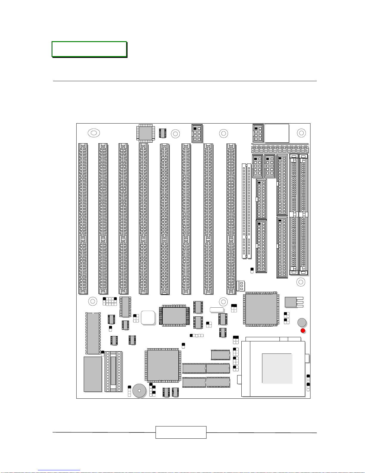
2.1 BOARD OUTLINE OF TF-486 3
2.2 CPU INSTALLING AND UPGRADING 4
2.3 JUMPER SETTING OVERVIEW 5
2.4 JUMPER LOCATION FOR TF-486 6
2.5 JUMPER SETTINGS SUMMARY FOR TF-486 7
2.6 JUMPER SETTINGS FOR TF-486 8
2.7 I/O CONNECTORS LOCATION FOR TF-486 14
2.8 I/O CONNECTORS SUMMARY FOR TF-486 15
2.9 SETTING STATUS INDICATORS AND CONTROL 16
CONNECTORS
2.10 I/O CONNECTORS DESCRIPTION 17
CHAPTER 3AWARD BIOS SETUP 23
3.1 RUNNING AWARD BIOS 23
3.2 CMOS SETUP UTILITY 24
3.3 STANDARD CMOS SETUP 25
3.4 BIOS FEATURES SETUP 30
3.5 CHIPSET FEATURES SETUP 33
3.6 POWER MANAGEMENT SETUP 35
3.7 PNP/PCI CONFIGURATION 37
3.8 LOAD BIOS DEFAULTS 39
3.9 LOAD SETUP DEFAULTS 39
3.10 INTEGRATED PERIPHERALS 39
3.11 SUPERVISOR / USER PASSWORD 41
3.12 IDE HDD AUTO DETECTION 41
3.13 HDD LOW LEVEL FORMAT 41
3.14 SAVE & EXIT SETUP 42
3.15 EXIT WITHOUT SAVING 43
APPENDIX A HOW TO USE WATCH-DOG TIMER 44
TERMS AND CONDITIONS
RMA SERVICE REQUEST FORM


TF-486 / 1
CHAPTER 1. INTRODUCTION
The TF-486 is i
documentation, certification and maintenance.
ESA's revision controlled motherboards reduce your long term costs for system testing,
environments where extensive testing or certification of the system is required.
computer telephony, industrial control, medical instrumentation and other application
control guidelines to provide a long and stable product life cycle. This makes it ideal for
One of the most important qualities of the TF-486 is that it is produced under strict revision
makes it an ideal alternative to expensive passive backplane system architectures.
motherboard. Its compact size, high reliability and large number of expansion slots
ISA cards or one can be PCI that is shared, on an industry standard Baby AT format
class of processors. It supports up to eight expansion cards, all of which can be full length
deal for a broad range of industrial applications utilizing the popular 486

INTRODUCTION
TF-486 / 2
1.1 SPECIFICATIONS
oProcessor :PGA socket for Intel®
80486 series, AMD®
486 series
SGS 486 series,and AMD®
& Cyrix®
5x86 series
oChipset :ALi M1487 / M1489
oBus Clock :20MHz, 25MHz, 33MHz, 40MHz and 50M Hz
oSystem Memory :Two 72-pin SIMM sockets up to 64MB EDO/FPM
DRAM
oL2 Cache Memory :0K cache, supports up to 512KB
oBIOS :128KB Award License BIOS
oFlash Memory Disk :Reserved one socket for Disk-On-Chip from M-Systems
support up to 144 MB Flash memory Disk-on-Chip
oIDE Drive Interface :Two Fast PCI bus IDE ports that support up to four IDE
devices
oFloppy Drive Interface :One FDD port that supports up to two floppy devices
oSerial Port :Two 16550 compatible FIFO RS-232 serial ports (Box
Header on board) with ESD clamping
oParallel Port :One multi-mode parallel port (ECP/SPP/EPP) (Box
Header on board) with ESD clamping
oRTC Battery :Dallas RTC battery or compatible
oMouse Connector :On-board 8-pin PS/2 Mouse header
oKeyboard Connector :On-board 8-pin Keyboard header
oExpansion Slot :Eight ISA and one PCI expansion slots
oWatchdog Timer :10 level time-out intervals
(0.5/1/2/4/8/16/32/64/128/256 sec)
oIR Interface :Support one IrDA header
oOperating Temperature :0°C~55°C (32°F~132°F)
oHumidity :10¢H~90¢H RH
oDimensions :257 mm X 222 mm

TF-486 / 3
CHAPTER 2.
JUMPER SETTINGS AND CONNECTORS
The Figure below shows the jumpers and connectors location on the TF-486
2.1 BOARD OUTLINE OF TF-486
JP4
TF-486
1
3
1
3
FAN1
ISA8
COM1
J1
1
ISA7
ISA6
ISA5
ISA4
ISA3
ISA2
ISA1
SIM1
SIM2
PIDE1
PCI1
PIDE2
RTC
BATTERY
¹
1
4 5
J4
J5
J2
J3
1
JP13
1 5
JP6
JP5
1 1
3 3
JP12
1 2
3 4 JP2
1 2
3 4
JP1
1
3 2
4
JP3
1 2
5 6
JP16
41
123
JP15
10
JP14
2
9H
L
3 1
11
COM2
PRT1
FDC1
SMI1
1
KB1
PMS1
PS1
ISB1
ISB2
ISB3
ISB4
ISB5
ISB6
ISB7
ISB8
PKB1
JP8
JP7
1 1
3 3
2
6
2
4
1 2
5 6
JP9
JP10
JP11
1
1
5
3
J6
S2

JUMPER SETTINGS AND CONNECTORS
TF-486 / 4
2.2 CPU INSTALLING AND UPGRADING
To upgrade to a higher power CPU, simply remove the old CPU and install the new one;
be sure to set the jumpers for the new CPU type and speed.
WARNING!
Disconnect the power cord from your system when you intend to work on it or
you plan to open the chassis of your IPC. Do not make connections when the
power is turned on, the sensitive electronic components could be damaged
by the sudden rush of power. Please only allow experienced electronics
technicians to do this job.
STATIC ELECTRICITY
PRECAUTION!
Caution! Computer components are very sensitive to damage from static
electric discharge. Always ground yourself to remove static charge build-up
before touching the boards in the computer. Use a grounding wrist strap at
all times. Place all electronic components on the anti-static pad for static-
dissipation or in a static-shielded bag when they are not in the chassis.
F

JUMPER SETTINGS AND CONNECTORS
TF-486 / 5
2.3 JUMPER SETTING OVERVIEW
In order to select the operation modes of your system, configure and set the jumpers on
the your MB to match the need of your application. To set a jumper, a plastic cap
containing metal contacts is placed over the jumper pins as designated by the required
configuration as listed in this section. A jumper is said to be “on ”or “1-2 ”when the
black cap has been placed on two of its pins, as show in the figure below:
A pair of needle-nose pliers is recommended when working with jumpers. If you have
any doubts about the best hardware configuration for your application, contact your local
sales representative before you make any changes. In general, you simply need a
standard cable or jumper to make most connections.

JUMPER SETTINGS AND CONNECTORS
TF-486 / 6
2.4 JUMPER LOCATION BOARD LAYOUT FOR TF-486
JP4
TF-486
1
3
1
3
JP6
JP5
1 1
3 3
JP12
1 2
3 4 JP2
1 2
3 4
JP1
1
3 2
4
JP3
1 2
5 6
JP16
41
123
JP15
10
JP14
2
9H
L
3 1
11
SMI1
1
JP8
JP7
1 1
3 3
2
6
2
4
1 2
5 6
JP9
JP10
JP11
1
1
5
3
S2

JUMPER SETTINGS AND CONNECTORS
TF-486 / 7
2.5 JUMPER SETTINGS SUMMARY FOR TF-486
JUMPERS
LOCATION FUNCTION
JP1 ~ JP2 Select CPU Voltage
JP3,JP4,JP9 ~ JP11 Select CPU Type
JP5, JP6, JP12 Select CPU Clock
JP7, JP8 Select L2 Cache Size
JP14, JP15 Select Watch-Dog Timer
JP16 Select M-System Address
S2 Clear CMOS Jumper
SMI1 External SMI Function Switch

JUMPER SETTINGS AND CONNECTORS
TF-486 / 8
2.6 JUMPER SETTINGS FOR TF-486
lJP1, JP2 : Select CPU Voltage
CPU Voltage JP1 JP2
3.3V (Default) 1-2, 3-4 OFF
5V OFF 1-2, 3-4
CPU Voltage: 3.3V (Default)
JP1
12
34
JP2
12
34
JP1
JP2 JP1
12
34
JP2
12
34
CPU Voltage: 5V
JP1
JP2

JUMPER SETTINGS AND CONNECTORS
TF-486 / 9
lJP3, JP4, JP9 ~ JP11 : Select CPU Type
CPU Type JP3 JP4 JP9 JP10 JP11
I486SX 1-2 1-2 OFF OFF OFF
I486DX/DX2/ODP;AmDX4-V8T 2-3 1-2 OFF OFF OFF
I486DX4/SL-ENHANCE 2-3 1-2 2-4 OFF 1-2, 3-4
Am486DX2-V8T 2-3 1-2 3-5 OFF OFF
Am486DE2-66V8T 2-3 1-2 2-4, 3-5 2-4 1-2, 3-4
Write Back Enhance CPU
AMD+Am486DX2/DX4-SV8B
AMD+Am5x86-P75 2-3 2-3 2-4
2-4, 3-5: AmDX2-SV8B;
AmD-X5-133/160
2-4: AmDX4-SV8B;
AmD-X5-150;
Intel W/B Enhance CPU
1-2, 3-4
Cyrix Cx486 (DX/DX2/DX4)-GP 2-3 1-2 1-3, 4-6 1-3, 4-6 L1 W/B OFF
Cyrix Cx486DX/DX2/DX4
Cx5x86 2-3 1-2 2-4 2-4 L1-W/B 1-2, 3-4
Note: AMD+ = Enhance SV8B (Internal W/B Cache)
CX486 = TI, STor SGS, IBM 486; (ST or SGS DX4= Intel DX4)
I486DX4/SL-ENHANCE (Default)
JP4
56
JP10
JP3
2
1
1
5
2
6
JP9
1
5
2
6
3
4
1
2
JP10
JP11
1
3
1
3
JP10
JP3
JP4
JP9
JP10
JP11 JP3
JP4
JP9
JP11
1
5
1
3
2
6
2
4
1
1
3
3

JUMPER SETTINGS AND CONNECTORS
TF-486 / 10
I486SX
1
5
2
6
JP9
1
5
2
6
3
4
1
2
JP10
JP11
1
3
1
3
JP10
JP3
JP4
I486DX/DX2/ODP;AmDX4-V8T
1
5
2
6
JP9
1
5
2
6
3
4
1
2
JP10
JP11
1
3
1
3
JP10
JP3
JP4
Am486DX2-V8T
1
5
2
6
JP9
1
5
2
6
3
4
1
2
JP10
JP11
1
3
1
3
JP10
JP3
JP4
Am486DE2-66V8T
1
5
2
6
JP9
1
5
2
6
3
4
1
2
JP10
JP11
1
3
1
3
JP10
JP3
JP4
AmDX2-SV8B;
AmD-X5-133/160
1
5
2
6
JP9
1
5
2
6
3
4
1
2
JP10
JP11
1
3
1
3
JP10
JP3
JP4
AmDX4-SV8B;
AmD-X5-150;
INTEL W/B Enhance CPU
1
5
2
6
JP9
1
5
2
6
3
4
1
2
JP10
JP11
1
3
1
3
JP10
JP3
JP4
Cyrix Cx486 (DX/DX2/DX4)-GP
1
5
2
6
JP9
1
5
2
6
3
4
1
2
JP10
JP11
1
3
1
3
JP10
JP3
JP4
Cyrix Cx486DX/DX2/DX4;
Cx586
1
5
2
6
JP9
1
5
2
6
3
4
1
2
JP10
JP11
1
3
1
3
JP10
JP3
JP4

JUMPER SETTINGS AND CONNECTORS
TF-486 / 11
JP6
JP12
3
31
1
4
2
1
3
JP5
JP12
JP5, JP6, JP12 : Select CPU Clock
CPU Bus
Clock JP5 JP6 JP12 CPU Core Clock
20M Hz 2-3 2-3 3-4
25M Hz 1-2 1-2 OFF SX-25, SX2-50, DX2-50
33M Hz 1-2 1-2 3-4, 1-2 SX/DX-33, DX2-66, DE2-66,DX4-100,5X86-100,X5-133
40M Hz 1-2 1-2 3-4 DX-40, DX2-80, DX4-120, X5-160
50M Hz 1-2 1-2 1-2 DX-50, X5-150
3
3
1
1
4
2
1
3
JP5
JP6
33M Hz (Default)
SX/DX-33,DX2-66,DE2-66,DX4-100,5X86-100,X5-133
JP5
JP6
JP12
20M Hz
33 1
1
4
2
1
3
JP5JP6
JP12
25M Hz
SX-25,SX2-50, DX2-50
33 1
1
4
2
1
3
JP5JP6
JP12
40M Hz
DX-40,DX2-80,DX4-120,X5-160
33 1
1
4
2
1
3
JP5JP6
JP12
50M Hz
DX-50,X5-150
33 1
1
4
2
1
3
JP5JP6
JP12

JUMPER SETTINGS AND CONNECTORS
TF-486 / 12
3
3
lJP7, JP8 : Select L2 Cache Size
L2 Cache JP7 JP8
128K 2-3 2-3
256K 2-3 1-2
512K 1-2 1-2
lJP14, JP15 : Select Watch-Dog Timer
Time Out Period JP14 JP15
0.5 sec 1-5 OFF
1 sec 2-6 OFF
2 sec 3-7 OFF
4 sec (Default ) 4-8 OFF
8 sec 8-12 OFF
16 sec 7-11 OFF
32 sec 6-10 OFF
64 sec 5-9 OFF
128 sec OFF 1-2
256 sec OFF 2-3
33 1
1JP7JP8
JP7
JP8
128K L2 Cache
33 11 JP7
JP8
256K L2 Cache
3
31
1JP7JP8
512K L2 Cache
1
1JP7
JP8
4 Sec (Default)
JP14
4
1
3 2
L
H
12
9
11
10
1
3
JP15
JP15
JP14
JP14
L
H
321
4
9
10
12 11
1
3
JP15
JP15
13
1
31
JP14
L
H
2
4
9
10
12 11
1
3
JP15
0.5 Sec
JP14
L
H
32
4
9
10
12 11
1
3
JP15
1 Sec
JP14
L
H
21
4
9
10
12 11
3
JP15
2 Sec
JP14
L
H
321
4
9
10
12 11
1
3
JP15
8 Sec
JP14
L
H
321
4
9
10
12 11
1
3
JP15
16 Sec
JP14
L
H
321
4
9
10
12 11
1
3
JP15
32 Sec
JP14
L
H
321
4
9
10
12 11
1
3
JP15
64 Sec
JP14
L
H
321
4
9
10
12 11
1
3
128 Sec
L
H
321
4
9
10
12 11
1
3
JP15
256 Sec

JUMPER SETTINGS AND CONNECTORS
TF-486 / 13
JP16 : Select Disk On Chip ( Flash Disk ) Address
Flash Disk Address JP16
C8000~CFFFF 1-2
D0000~D7FFF 3-4
D8000~DFFFF 5-6
Default 2-4
lS2 : Clear CMOS Jumper
Clear CMOS Jumper S2
Normal (Default ) OFF
Clear CMOS 1-2
lSMI1 : External SMI Function Switch
SMI Function SMI1
Disable OFF
Enable ON
JP16
D0000~D7FFF
D8000~DFFFF
C8000~CFFFF
1 2
56
6
JP16
1
3
54
2
Spare Jumper
JP16
S2
Clear CMOS
Normal 2
1
S2
2
1
S2
SMI1
Enable
Disable 2
1
SMI1
2
1
SMI1

JUMPER SETTINGS AND CONNECTORS
TF-486 / 14
2.7 I/O CONNECTOR LOCATION FOR TF-486
TF-486
FAN1
COM1
J1
1
PIDE1
PIDE2
1
4 5
J4
J5
J2
J3
1
COM2
PRT1
FDC1
PMS1
PKB1
J6
JP13
1 5
Table of contents