User Guide — EP9134_UG V0.2
Explore Confidential Proprietary
NON-DISCLOSURE AGREEMENT REQUIRED
8
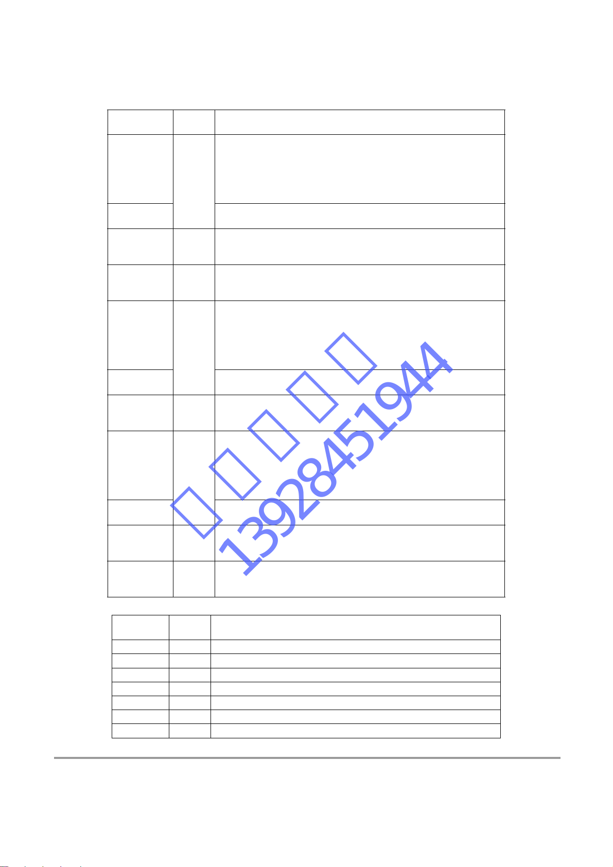
TX01-
TX01+
TX11-
TX11+
TX21-
TX21+
Analog
Differential Data Output Pairs for transmitter port 1
TXC1-
TXC1+ Differential Clock Output Pairs for transmitter port 1
HTPLG1 IN
Hot Plug Input
This pin is used to monitor the "HOT PLUG" signal for tansmitter port 1. Note:
This input is only 3.3V tolerant and has no internal debouncer circuit.
EXT_SWING01 Analog
Voltage Swing Adjust for Port 0/1. A resistor should tie this pin to AVCC. This
resistance determines the amplitude of the voltage swing. 560:is
recommended.
TX02-
TX02+
TX12-
TX12+
TX22-
TX22+
Analog
Differential Data Output Pairs for transmitter port 2
TXC2-
TXC2+ Differential Clock Output Pairs for transmitter port 2
HTPLG2 IN
Hot Plug Input
This pin is used to monitor the "HOT PLUG" signal for tansmitter port 2. Note:
This input is only 3.3V tolerant and has no internal debouncer circuit.
TX03-
TX03+
TX13-
TX13+
TX23-
TX23+
Analog
Differential Data Output Pairs for transmitter port 3
TXC3-
TXC3+ Differential Clock Output Pairs for transmitter port 3
HTPLG3 IN
Hot Plug Input
This pin is used to monitor the "HOT PLUG" signal for tansmitter port 3. Note:
This input is only 3.3V tolerant and has no internal debouncer circuit.
EXT_SWING23 Analog
Voltage Swing Adjust for Port 2/3. A resistor should tie this pin to AVCC. This
resistance determines the amplitude of the voltage swing. 560:is
recommended.
Table 2-5 Power and Ground Pins
NAME IN /
OUT DESCRIPTION
VDDE PWR Digital Power, 3.3V
VSSE GND Digital Ground
VDD18 PWR Core Power, 1.8V
VSS GND Core Ground
AVDD PWR Analog Power, 3.3V
AVSS GND Analog Ground
PVDD PWR Analog Power for PLL, 3.3V
Table 2-4 Transmitter Pins
NAME IN /
OUT DESCRIPTION