Farnell L30A User manual

Farnell
SUPPLY UNITS
STABILISED VOLTAGE CURRENT
L30 SERIES Issue 4.
INSTRUCTION BOOK

FARNELL INSTRUMENTS LIMITED
SUPPLY UNITS
STABILISED VOLTAGE CURRENT
L30 SERIES Issue 4.
FARNELL INSTRUMENTS LTD.
Sandbeck Way, Wetherby. Yorkshire LSZ2 4DH
Telephone 0937 3541 3/6

MCMXCVII
SECTION I
CONTENTS
INTRODUCTION Page No
I
SECTION II OPERATING INSTRUCTIONS 2
SECTION III CIRCUIT DESCRIPTION ,
.
4
SECTION IV SPECIFICATION .. .. 6
SECTION VINTERNAL ADJUSTMENTS 8
SECTION VI TYPICAL PERFORMANCE .
.
9
SECTION VII MECHANICAL SPECIFICATION .. 16

SECTION I
INTRODUCTION
This manual covers the MK II L30 series of D.C. stabilised
voltage/current supply units. The circuit diagram contained in
the manual is for the particular unit type supplied.
Twin units are designated L30 -/T and consist of two appro-
priate L30 units mounted in the one case. The two outputs are
completely independent. They may be used as separate supplies
or alternatively may be connected in series or parallel, to provide
higher output voltages or currents than can be obtained from a
single L30 supply.
The semiconductor complement of these supplies is silicon
throughout, permitting operation to 45"C ambient at full specified
output.
The output voltage is adjusted by means of two controls on
the front panrl marked "COARSE "and "FINE."
The o-itput voltage or current is monitored by aswitched
voltmeter/ammeter.
Overload protection is provided to protect the power unit and
apparatus, being supplied by limiting the output current to aset
valup. This value is adjustable from zero to the maximum current
of the unit by means of acontrol on the front panel marked
"CURRENT LIMIT." The circuit will automatically reset when
the overload is removed.
The instrument will operate from mains supplies of 210, 220,
230 and 240v. A.C. at 50/60 Hz.
(An alternative instrument is manufactured for use with mains
supplies of 105—120v.).
Certain units in the range are fitted with internal overvoltage
protection (see Section IV) when the unit output exceeds alevel
set by means of afront panel control, the unit output is clamped
to alow value by means of athyristor crowbar circuit.
'

SECTION II
OPERATING INSTRUCTIONS
Care should be taken to ensure that the input selector on the
rear of the unit is set to match the mains supply from which the
supply is to be operated.
The mains lead is wired as follows :
—
BROWN Mains Line.
BLUE Mains Neutral.
GREEN/YELLOW Earth.
NORMAL CONSTANT VOLTAGE OPERATION
Before connection to the mains supply is made, the output
"ON/OFF" switches, should be set to "OFF". The link on the
bottom of the unit should be in the "CV" position.
With the mains supply connected, the mains "ON/OFF" switch
is set to "ON" and the mains indicator lamp should light.
With the meter switch set to "VOLTS", the required output
voltage is selected by adjusting the "COARSE" and "FINE"
voltage controls on the front panel and the current limit control
set to maximum' (fully clockwise). Unless use of the current
limiting is to be made, the load is now connected and the output
"ON/OFF" switch set to "ON". Output current can he monitored
by setting the meter switch to "CURRENT".
CURRENT LIMIT SETTING
If acertain maximum current must not be exceeded or a
roughly constant current is required, use may he made of the
current limiting facility, maximum current being set by the front
panel control marked "CURRENT LIMIT".
(1) APPROXIMATE CONSTANT CURRENT OPERATION
With the mains supply connected to the unit, mains and output
switches set to "ON", the meter switch set to "CURRENT" and
the output voltage controls set to maximum, the positive output
terminal is linked to the negative output terminal and the current
limit control set to give the required current. On removal of the
link and connection to the load, the unit will give aroughly
constant current over avoltage range from zero to the maximum
specified output voltage depending on the bad resistance.
(2) CURRENT CEILING OPERATION
If acertain maximum current is not to be exceeded then the
setting up procedure is as follows :—
With the mains supply connected to the unit, mains and output
switches to "ON", the meter switch set to "CURRENT" and the
voltage controls set to the required value, avariable load is
connected to the unit and is set to give the required maximum
current. The current limit control is then adjusted until the
current just starts to fall. The unit will now prevent more current
than this value being drawn from it. It is advised that this
current "ceiling" is set to approximately 10% in excess of the
expected maximum to prevent any modification to the voltage
regulation characteristic. The variable load is now disconnected
and the unit is ready for use.
ACCURATE CONSTANT CURRENT OPERATION
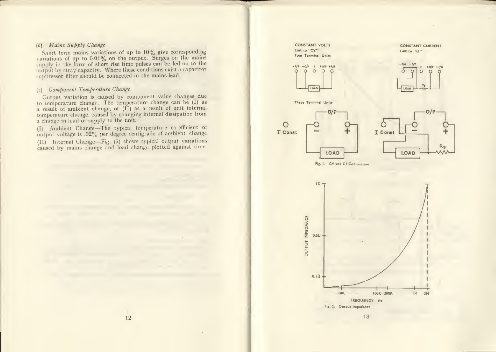
(See Fig. 1}
If afixed resistor Rs is connected between the positive output
terminal and the "I const" or "—F/B" terminal, the link on the
bottom of the unit set to CI, and the load Rl between the "I const"
or "—F/B" terminal and the "O/P -ve" terminal, then the unit
will keep the voltage across Rs constant. Thus aconstant current
will flow in Rs. Since Rl is in series with Rs, the same current
will flow in Kt..
The value of Rs is given by :— See Errata and
VAddenda -Page 15
Rs =Rl max.
Iout
Where Vis the maximum specified output voltage of the unit.
Rs must have apower rating well in excess of the power it
dissipates in order that the change in resistance due to self heating
is minimised.
The power dissipated in Rs is given by :
—
P(Rs) =Iout- Rs.
Rs is then connected between the "0/P +"and "I const"
terminals. The "I const" or "—F/B" terminal is shorted to the
"O/P—" terminal and the "VOLTAGE ADJUST' controls set
until the meter reads the required output current. The "short"
is then removed and the load connected in its place. The output
current will be constant with the same specification as the constant
voltage specification with the load varying from zero to Rl max.
note i
—
The front panel "CURRENT LIMIT" control should be set
to maximum for this mode of operation.
3

FOUR TERMINAL OPERATION
Certain units have been provided with four terminal output
to enable the correction of resistive drop mconnecting leads.
When this correction is not required, the +F/B and +0/P
terminals should be linked together and the —¥/\i and —O/P
terminals should be linked together. When correction is required
the links should be removed. The load should be connected to
the +0/P and —O/P terminals and the +F/B and —F/B
terminals connected through separate wires to the appropriate
ends of the load. It may be necessary to decouple at the load
with an electrolytic capacitor to prevent instability in this
connection.
OVER-VOLTAGE PROTECTION
On units fitted with over-voltage protection the over-voltage
trip level adjustment is on the front panel of the unit, and the
current limit control on the back of the unit.
To set agiven trip level, set the output voltage to this level,
and adjust the "OVERVOLTAGE" control until the output
voltage falls to alow level.
Set the voltage adjustment controls fully anti-clockwise, the
output (or mains) switch to off, and then on. This resets the
overvoltage trip. Re-adjust the output voltage controls to give
the required operating voltage.
SECTION III
CIRCUIT DESCRIPTION
The circuit employs series regulator transistors driven via
emitter followers from adifferential amplifier which compares the
voltage of azener diode reference with aproportion of the output
voltage derived from aresistive potential divider.
The mains supply is connected via fuse Fl, SW1 and the input
selector to MT1. The main secondary winding supplies abridge
rectifier, reservoir capacitor system which provides the main
unregulated D.C. line. The positive line is connected via the
series regulator transistors and SW2 to the positive output
terminal. The negative line is connected via fuse F2 to the
negative output terminal.
Supplies for the amphfier and reference section are derived
from the auxiliary 36 volt secondary winding, via rectifier diodes
D5 and D6 and smoothed by capacitor C2. The unstabilised
reference line is fed to zener diode Zl via resistor R2, The semi-
sta bilised voltage across Zl is fed to zener diode Z2 and Z4 via
R3 providing 10 volts positive and approximately 5volts negative
with respect to the positive output terminal. The voltage across
Z2 feeds the reference zener diode Z3 and potential divider chain
R7, Tl ,PI and P2, via Resistor R4.
The base of VT1 and the negative of Z3 are connected to the
positive output terminal. R7 and Tl are connected between the
positive of Z3 and VT2 base via R8. Any difference between the
voltages at VT1 and VT2 bases is amplified at the collector of
VT2 and applied to VT3 base. After further amplification at
VT3 collector the signal is applied to the emitter followers of the
series regulator stage in such asense as to oppose the original
signal at VT1 and VT2 bases. The action of the loop is therefore
to maintain zero voltage between VT1 and VT2 bases.
i

Output voltage is determined by :—
Vref (PI +P2)
R7 +Tl
Overload protection is provided by VT4 and VT8. As output
current increases, the voltage drop across R17 increases until
the base of VT4 is sufficiently positive to turn it on. This diverts
current from the series regulator stage, thus reducing the output
voltage. On further increase in load, VT4 will maintain aroughly
constant voltage drop across El 7which gives aroughly constant
current output. The point at which the initial current limit
occurs is set by P3 and the maximum current limit point is set
byT2.
OVERVOLTACE PROTECTION
On units fitted with overvoltage protection, this is provided
by means of aThyristor "crowbar" connected across the output
terminals, and driven from avoltage comparator amplifier which
compares afraction of the output voltage with areference zener
diode. Rla, Zla, R7a and VTla, comprise aconstant current
source to feed the reference zener diode Z2a, Z9a and R10A feed
afraction of this voltage to VT3a base. VT3a and VT4a are the
comparator transistors, the base of VT4a being fed from potential
divider Pla, R6a and R13a. If the output voltage exceeds alevel
determined by this potential divider VT4a conducts, driving
VTZa on. The drive then available from.VT2a collector then
fires SCRla which short circuits the output terminal.
)SECTION IV
SPECIFICATION
Mains Supply
210, 220, 230 or 240 volts 50/60 Hz.
Alternatively, instruments may be
120 volts 50/60 Hz.
Output Voltage and Current Ranges
SINGLE UNITS
supplied for 105, 110,
L30A —50V, 0.5A.
L30B —30V. 1A.
L30C —10V. 3A.*
L30D —30V. 2A.
L30E —30V. 5A.
L30F —12V. IDA.*
TWIN UNITS
L30AT 2x0--50V. 0.5A
L30BT 2x0--30V. 1A.
L30DT 2x0--30V. 2A.
Fitted with overvoltage protection.
Mains Variation Tolerated
±10% of Nominal.
Output Voltage Variation for ±10% Mains Change
Less than .01% or lmV whichever is the greater—short term.
Less than .02% or 2mVwhichever is the greater—long term.
Output Voltage Variation for Zero to Full Load Change
Less than .01% or 2mVwhichever is the greater—-short term.
Less than .02% or 4mV whichever is the greater—long term.

Output Current Variation for 10% Mains Change (Accurate
Constant Current Operation)
Less than .01 %or 1mA whichever is the greater—short term.
Less than .02% or 2mA whichever is the greater—long term.
Output Current Variation for Zero Resistance to Max. Resistance
Change (Accurate Constant Current Operation)
Less than .01%—short term.
Less than .02%—long term.
Output Current Variation for 10% Mains Change (Approximate
Constant Current Operation)
Less than 1%—short term.
Less than 2%—long term.
Output Current Variation for Zero Res.—Max. Res. Change
(Rough Constant Current Operation).
Less than 2%—short term.
Less than 3%—long term.
Ripple Voltage at Full Load
Less than ImV peak to peak.
Ripple Current at Full Load
Less than ImA peak to peak.
Overload Protection
Current Limiting.
Overvoltage Protection
Thyristor "crowbar" trip. Trip level adjustment approx. 3.2V.
to 14V., temp, coefficient of trip level 0.04% /°C. typical.
Max. Operating Temperature
45°C.
Temperature Coefficient
±0.02% per °C. Typical.
Output Impedance
See Fig. (2). 8
SECTION V
INTERNAL ADJUSTMENT
Units are set up before leaving the factory, but in the event
of future mis-alignment the setting-up procedure is as follows :—
VOLTAGE ADJUSTMENTS
(1) An accurate voltmeter is connected between the "O/P—
"
and "O/P \-" terminals, with an f.s.d. compatible with the
specified maximum output voltage of the unit.
With the unit switched on, the link on the bottom of the unit
set to "CV" and the "VOLTAGE ADJUST" controls fully
clockwise, TI, on the circuit board, is adjusted to give the
specified maximum output voltage.
(2) With the meter switch set to "VOLTS", T3 is now adjusted
so that the front panel meter reads full scale.
CURRENT ADJUSTMENTS
(1) An accurate ammeter with an f.s.d. compatible with the
specified maximum output current of the unit, is connected in
series with avariable load between the "0/P+" and "O/P—
"
terminals.
With the unit switched on, the link on the bottom of the unit
set to "CV" and the "CURRENT LIMIT" control fully clock-
wise, the load is adjusted to give 10% in excess of the specified
maximum output current. T2 is then adjusted until the current
just starts to fall.
{2) With the meter switch set to "AMPS", the load is re-adjusted
to give the specified maximum output current and T4 is adjusted
so that the front panel meter reads full scale.
9

SECTION VI
TYPICAL PERFORMANCE AND APPLICATIONS
1. VOLTAGE PROGRAMMING
All units can be programmed by means of external resistors to
any voltage below the specified maximum voltage, the program-
ming terminal being the "1 const" or "—F/B" terminal. The
link on the bottom of the unit is set to "CI" and the "VOLTAGE
ADJUST" controls turned fully anticlockwise. The programming
resistor should now be connected between the "I const" and
"O/P—"terminals.
The value of programming resistor is given by :
—
25-25
Rprog —XVrequired, Kilohms (L30A)
Rprog
50
25,25
30
5.1
-X Vrequired, Kilohms (L30B, D&E}
Rprog =—X Vrequired, Kilohms (L30C)
10
The tolerance on Vrequired for an accurate Rprog is ±10%.
In order to obtain greater accuracy, the voltage of the reference
zener-diode Z3, (V ref) and the resistance of R7 -• Tl must be
determined. Rprog is now given by :
—
R7 -1- Tl
Rprog —XVrequired, ohms
Vref
The tolerance on Vrequired for an accurate Rprog is now
the tolerance on the Vref measurement plus the tolerance on
the R7 H- Tl measurement.
2. SERIES OPERATION
Units may be connected in series ONLY IN THE "CV"
MODE OF OPERATION.
3. PARALLEL OPERATION
[A) "CV" OPERATION
Units which are set to approximately the same output voltage
may be connected directly in parellel. On increasing load, the
unit having the highest output voltage will cany the load until
it current limits, thereafter the unit having the next highest
10
voltage will supply the extra current until it limits, and so on.
Atypical output characteristic for aparallel combination of three
units is shown in Fig. (3).
The characteristic shows aseries of descending steps in output
voltage at the current limit points of individual units, the ampli-
tude of the steps depends on how closely the output voltages have
been set and it may not be possible to adjust this to better than
50mV.
It is recommended that not more than three units are paralleled
in this way.
(B) "CI" OPERATION
Units can be connected directly in parallel in either "APPROX-
IMATE CI" or "ACCURATE CI" operation, the load current
being the sum of the two output currents, Fig. (I) shows the connec
tions for "ACCURATE CI" operation.
4. TYPICAL PERFORMANCE
Stability
Output variations are due in the main to the following causes :
—
Load Change.
Mains supply change.
Component temperature change.
(a) Load Change
(I) Steady load—For achange in steady load from zero to full
load, the typical change is :—ImV at full voltage output.
(II) Transient Response—The typical response to apulsed load
is shown in Fig. (4),
(III) Output Impedance.
For alternating load superimposed on asteady load, the output
impedance of the supply increases with frequency due to the fall
off in gain of the amplifier until it is determined only by the
capacitor across the output terminals.
Atypical output impedance/frequency curve is shown in Fig. (2)
11

(tV) Mains Supply Change
Short term mains variations of up to 10% give corresponding
variations of up to 0.01% on the output. Surges on the mains
supply in the form of short rise time pulses can be fed on to the
mtput by stray capacity. Where these conditions exist acapacitor
suppressor filter should be connected in the mains lead.
(c) Component Temperature Change
Output variation is caused by component value changes due
to temperature change. The temperature change can be (I) as
aresult of ambient change, or (II) as aresult of unit internal
temperature change, caused by changing internal dissipation from
achange in load or supply to the unit.
(I) Ambient Change—The typical temperature co-efficient of
output voltage is .02% per degree centigrade of ambient change
(II) Internal Change—Fig. (5) shows typical output variations
caused by mains change and load change plotted against time.
CONSTANT VOLTS
Link to "CV"
Four Terminal Units
-f/s -o/p E+Q/P +F/B
Q Q OQQ
CONSTANT CURRENT
Link to "CI"
-f/b -a/r
L-j LOAD I
e+cyp +f/h
OQQ
LLjvv^
Three Terminal Unfit
-O/p 1
IConst j—
o
o—
1
+
LOAD
1Const
ro/p 1
I
j-2 $-
LOAD Rs
Fig. I. CV and CI Goftnectio
Ifi-T
J
z
<
a
r0.5S! ..
S
0.II1--
00 K100 KIN 1M
12
FREQUENCY Mi
Fif. 2. Output Impedance
13

<
o
>
O
OUTPUT CURRENT
Fif. 3. Parallel Operation
S
O
3
f.NL
TIME
Fif, 4. Pulifl Retpomc
14
K
E
o
wv--
Fij. 5. Tyfllttl Omput Volnf# Vtt-lfilon
ERRATA AND ADDENDA
AlTFKNVnVE COMPONENT TO THOSE LISTED ON CIRCUIT
DIAGHAM MAY BE USED IN THE EVENT OF SUPPLY DIFFICULT-
IES. MAJOR CHANGES TO THE DESIGN OR MANUAL AKE LISTED
BELOW ;—
In practice the voltage across Rs should not
be less than 1volt, so that Rs should
have avalue of. not less than:-
Rs min =
Iout
It should also be noted that the sum of the
voltages across Rs and R^ must not
exceed the maximum ratea output voltage of
the unit for the unit to meet its specification.
-15 -

\
1
'
3
o
rr
no
Tl~.
3
O
rrr
coo
M
-r uM171 u>
:..
-..1
3M
OOIE
£
IJ
-A -j ^n
A.J
Lin 8•a
mJ1 S°
J> #m
1i
Kj I
**
^I«L> ore
h
>1
£
ft
"r
L.
^
r
]
L
D]
O
a.'
-o
JTS LTD. WETHERBY,
DRAWING No.
3szx aou
*
^**"
r
w

USt-
ON
<n
VT
MISC
TRACED
CHECKED
DRAWN
:;DIP
C2». l.73
ISS.
^-•2-?3
^-*-7Z.
DATE
ft^n3
Qzobl
at >s^-z
MOD, No
NOTt
CAPACITOR VALUES GIVEN IN pF.
RESKTOIH VALUES IN II
©REFEIftS TO CCT. BO,
PIN CONNECTION No*
VT
MISC
FARNELL INSTRUMENTS LTD. WETHERBY, YORKS.
iDRAWING No.
3SZX QOH

USK
ON
o
QZ
VT
MISC
.TS. 240 )
%
/r
/
/
/i~
/
.\k
/A/s
/777
*i
i
-—
•
-r
i
I
-*—•—»
-• i
*v ri
irJ'
iI
I
ii•
i
L|-|-
DL1
L
TRACED
CHECKED
DRAWN
B
ISS.
*•? -1- T3
2» I7.3
>ATl '
VT
J=
o
,-Ly^
H5
c
-o
-o
-O I?
-o
-Q-
;
220*]
i
1
r^n
i-
j
J
tO i,
ONt 2
Qua
02053
MOD No.
NOTE :—
CAPACITOR VALUES GIVEN IN
RESISTOR VALUES IN tl
@REFERS TO OCT. BD,
PUN CONNECTION Noi
MF. FARNELL INSTRUMENTS LTD. WETHERBY, YORKS
DRAWING No,
3

FARNELL INSTRUMENTS LIMITED SANDBECKWAYWETHERBY YORKSHIRE LSZ2 4DH TELEPHONE 0937 3541
This manual suits for next models
9