FEC FEB-9455 User manual

FEB-9455 Intel 945GME 5.25” ESB
User’s Manual Rev.01, Aug. 2009

FEB-9455 User’s Manual
2
All rights reserved. No part of this publication may be reproduced in any form or by
any means, without prior written permission of the publisher.
All trademarks are the properties of the respective owners.
All product specifications are subject to change without notice.
None
Packing List
Statement

FEB-9455 User’s Manual
3
Contents
Chapter 1 Product Information..........................................................................................4
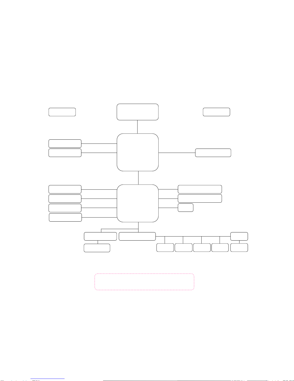
1.1 Block Diagram...................................................................................................................4
1.2 Features.............................................................................................................................5
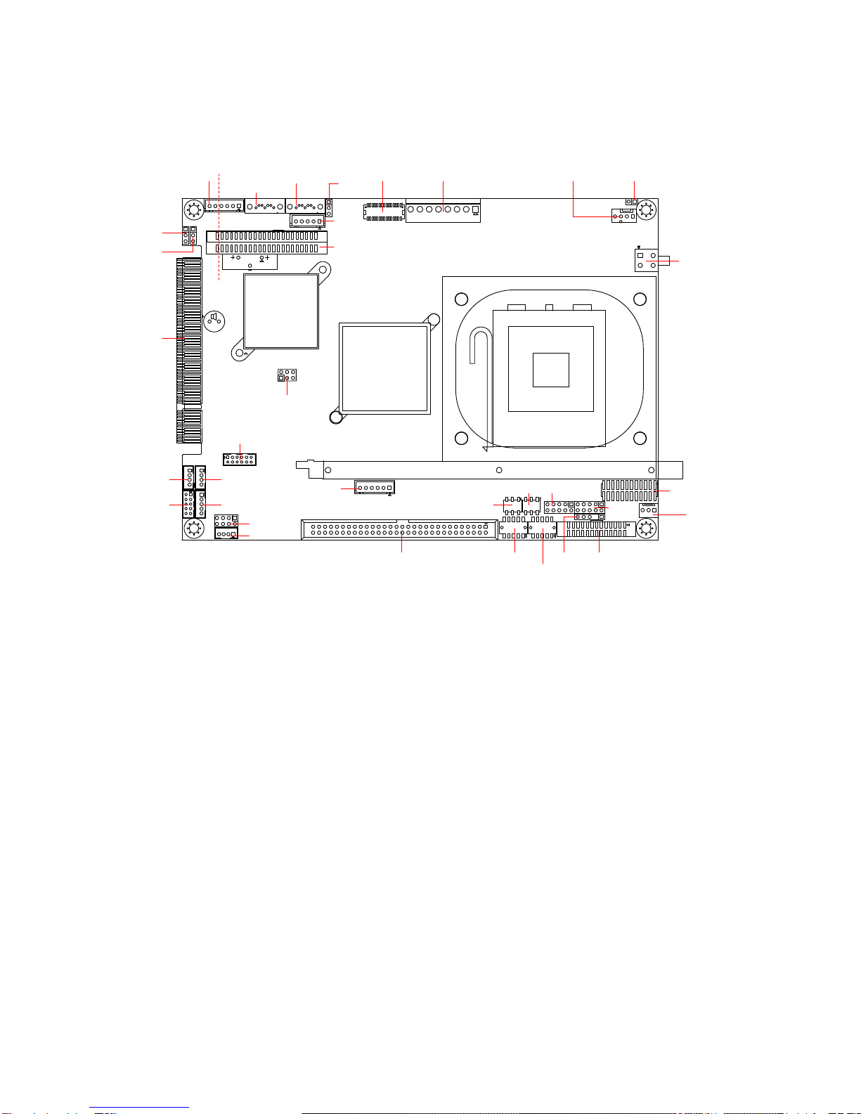
1.3 PCB Layout........................................................................................................................7
1.4 Jumper Setting..................................................................................................................8
1.5 Connector Function List.................................................................................................10
1.6 Internal Connector Pin Define......................................................................................11
Chapter 2 BIOS Setup........................................................................................................19
2.1 Main Menu.......................................................................................................................19
2.2 Standard CMOS Features.............................................................................................20
2.3 Advanced BIOS Features..............................................................................................21
2.4 Advanced Chipset Features..........................................................................................23
2.5 Integrated Peripherals ...................................................................................................25
2.6 Power Management Setup ...........................................................................................30
2.7 PnP/PCI Configurations.................................................................................................33
2.8 PC Health Status............................................................................................................34
2.9 Frequency/Voltage Control............................................................................................35
2.10 Load Fail-Safe Defaults...............................................................................................36
2.11 Load Optimized Defaults.............................................................................................37
2.12 Set Supervisor Password............................................................................................38
2.13 Set User Password......................................................................................................39
2.14 Save & Exit Setup........................................................................................................40
2.15 Exit Without Saving......................................................................................................41
Chapter 3 Drivers Installation..........................................................................................42
3.1 Intel Chipset Device Software ......................................................................................42
3.2 Intel Graphic Media Accelerator Driver.......................................................................45
3.3 LAN Driver.......................................................................................................................48
3.4 Audio Driver.....................................................................................................................50
Appendix-A Watchdog.......................................................................................................51
Appendix-B GPIO................................................................................................................51

FEB-9455 User’s Manual
4
Chapter 1 Product Information
This chapter introduces the product features, jumper and connector information.
1.1 Block Diagram
Intel LGA775
Intel 945G/GC
VRD10/11 CK410
VGA
LVDS_CH7308
FSB 533/800/1066MHz
DDR2 400/533/667 MHz
DMI
S/IO W83627EHG
IDE / CF
USB x8
COM1
SPI
DIOPrinterKB/MS IrDA
LAN_RTL8102E
CODEC_ALC662
Intel ICH7
USB
SATA
LPC
PCI
SPI
DDR2(240 Pin)
SATA x2
PCI-E
SDVO
PCI
IDE
S/IO F81216D
COM3/4/5/6
HDA
COM2
MIO (Multi IO Connector)
COM1, COM2, COM3, COM4, VGA, LAN, PS2 KB/MS

FEB-9455 User’s Manual
5
1.2 Features
System
Processor / Chipset
Processor Intel LGA775 Socket, Intel Core 2 Duo,
Pentium 4 processor in the 90 nm process
in the LGA775 Land Grid Array package or
Pentium D processor (supports 775-Land
package)
FSB 533/800 MHz (945G support 1066MHz)
Chipset Intel 945G/GC + ICH7
BIOS AWARD 16Mb SPI
Memory Technology DDR2 400/533/667 MHz SDRAM
Max. Capacity Up to 2GB (945G support up to 4GB)
Socket 1 x 240 DDR2 DIMM
Display
Chipset Intel 945G/GC integrated GMA950
VRAM Shared with 224MB system memory
Resolution Analog Display: Up to 2048 x 1536 (QXGA)
LVDS Chrontel CH7308 18/24 bit, Dual Channel
LVDS
Resolution Digital LVDS: Up to 1600 x 1200 (UXGA)
Dual Display CRT + LVDS
Ethernet Interface 10/100 Mbps ( GbE Optional)
Controller Realtek 8102E
(Realtek RTL8111C Optional)
Audio Interface High Definition Audio
Controller Realtek ALC662 HD CODEC
SATA Max. Data
Transfer Rates 300 MB/s
Port 2
IDE Mode IDE (44 Pin), Ultra ATA100/66/33
Channel 2
Compact Flash 1, Compact Flash Type I/II
Expansion Slot PCI 4 with Riser Card

FEB-9455 User’s Manual
6
Internal Connector
VGA 1
LVDS 1
LAN 1
USB 2.0 8
COM 6[3(RS232), 2(RS232, supply 5V/12V),
1(RS232/422/485, supply 5V/12V)]
Parallel 1
Audio Header 1(Line-In, MIC-In)
Audio Amplifier 1 [6W(4Ω) stereo]
Compact Flash 1 (Bottom Side)
IrDA 1
PS2 1 (K/B by MCR)
Digital IO 8Bit GPIO (4 IN + 4 OUT)
Power Type ATX(8Pin)
Watchdog Timer Interval Programmable 1~255 sec./min.
Output System reset
Environment
Operating
Temp. -5°C~ 60°C (23°F ~ 140°F)
Storage Temp. -20°C~ 80°C (-4°F ~ 176°F)
Relative
Humidity 0%~ 95% (non-condensing)
Form Factor Dimension
(L x W) 203mm x 146mm

FEB-9455 User’s Manual
7
1.3 PCB Layout
5
1
1
5
14
7
14
7
1
2
43
44
6
5
1
2
1
212
11
8
7
1
2
1
4
4
4
12
10 9
29
30 2
1
34
2
8 7 6 5 4 3 2 1
1
14
13
26
1
2
9
10
1
2
9
10
1
5
2
6
1
5
26
10
2
9 1
10 2
91
59
60 2
1
16
1
6
JP2
JP3
SATA_PWR1 SATA1 SATA2 JP1
INV1
IDE1
LVDS1 PWR1 BT1CPUFAN1
PWR2
DIMM1
AUXFAN1
JLVDS
LAN
AUDIO2
AUDIO1
MCR1
MIO1
JP5 JP6 JFRONT1
DIO1
IR1 LPT1COM5
COM6
USB2USB1
USB3 USB4
PCI
JP4
CF1
(Bottom Side)

FEB-9455 User’s Manual
8
1.4 Jumper Setting
JP1:LCD Power (+3.3V / +5V) Select
Pin No. 1-2 2-3
Function LCD Power +3.3V (Default) LCD Power +5V
Jumper
Setting
JP2:Compact Flash ( Master / Slave ) Select
Pin No. 1-2 2-3
Function Master Mode Slave Mode (Default)
Jumper
Setting
JP3:CMOS Clear
Pin No. 1-2 2-3
Function Normal Operation (Default) Clear CMOS Contents
Jumper
Setting
1
2
3
1
2
3
1
2
3
1
2
3
1
2
3
1
2
3
1
2
3
1
2
3
1
2
3
1
2
3
1
2
3
1
2
3

FEB-9455 User’s Manual
9
JP4:COM2 (RS-232/RS-422/RS-485) Select (1/3)
Pin No. 5-6, 11-13, 12-14, 19-21, 20-22 3-4, 9-11, 10-12, 17-19, 18-20
Function RS-232 (Default) RS-422
Jumper
Setting
JP4:COM2 (RS-232/RS-422/RS-485) Select (2/3)
Pin No. 1-2, 9-11, 10-12, 23-24 15-16
Function RS-485 RS-422 RX 100Ω Termination
Jumper
Setting
JP4:COM2 (RS-232/RS-422/RS-485) Select (3/3)
Pin No. 7-8
Function RS-422 TX 100Ω / RS-485
Termination
Jumper
Setting
JP5 / JP6:COM5 / COM6 (5V/12V/RI) Select
Pin No. 1-2 3-4 5-6
Function +5V Modem Ring In
(Default) +12V
Jumper Setting
6 4 2
5 3 1
6 4 2
5 3 1
6 4 2
5 3 1
6 4 2
5 3 1
6 4 2
5 3 1
6 4 2
5 3 1
23 1
24 2
23 1
24 2
23 1
24 2
23 1
24 2
23 1
24 2
23 1
24 2
23 1
24 2
23 1
24 2
23 1
24 2
23 1
24 2

FEB-9455 User’s Manual
10
1.5 Connector Function List
Connector Function Note
AUDIO1 6W amplifier Line-out Connector
AUDIO2 Line-in, MIC-In Connector
AUXFAN1 System FAN 3-pin Connector
BT1 Power Button Connector
CF1 Compat Flash Connector
CPUFAN1 CPUFAN 4-pin Connector
COM5,COM6 Serial port Connector with Box-header
DIMM1 DDR2 240 Pin Slot
DIO1 Digital I/O with Pin-header
IDE1 HDD IDE Connector (Supply +5V)
INV1 LCD inverter Connector
IR1 IrDA Connector
MIO1 Multi IO Connector
MCR1 MSR Connector with Box-header
LAN LAN Connector with Pin-header
LPT1 Printer Connector with Pin-header
LVDS1 LVDS Connector
PCI PCI Connecting Finger
PWR1 ATX Connector with extension cable
PWR2 ATX 4 Pin Connector
SATA1, SATA2 SATA Connector
SATA_PWR1 SATA Power Connector
USB1, USB2,
USB3, USB4 USB Connector with Pin-header

FEB-9455 User’s Manual
11
1.6 Internal Connector Pin Define
AUDIO1:Audio Amplifier Output with Box-header (2.0 mm)
Pin No. Signal
1 Audio Amplifier Out Right
2 Ground
3 Ground
4 Audio Amplifier Out Left
AUDIO2:Audio signal Connector with Pin-header (2.0 mm)
Pin No. Signal
1 MIC1-IN-L
2 LINE1-IN-L
3 MIC1-JD
4 LINE1-JD
5 Ground
6 Ground
7 MIC1-IN-R
8 LINE1-IN-R
AUXFAN1:System FAN 3 Pin Connector
Pin No. Signal
1 Ground
2 Fan Power (+12V)
3 Speed Sense
BT1:Power Button with Pin-Header (2.54mm)
Pin No. Signal
1 PSIN#
2 Ground
CPUFAN1:4Pin FAN Connector
Pin No. Signal
1 Ground
2 Fan Power (+12V)
3 Speed Sense
4 Control

FEB-9455 User’s Manual
12
COM5, COM6:Serial Port with Box-header (2.0 mm)
Pin No. Signal Pin No. Signal
1 DCD 2 DSR
3 RXD 4 RTS
5 TXD 6 CTS
7 DTR 8 RI/+5V/+12V
9 Ground 10 NC
DIO1:Digital I/O Connector with Pin-header (2.54mm)
Pin No. Signal Pin No. Signal
1 DIO-Out3 2 DIO-In3
3 DIO-Out2 4 DIO-In2
5 DIO-Out1 6 DIO-In1
7 DIO-Out0 8 DIO-In0
9 Ground 10 +5V

FEB-9455 User’s Manual
13
IDE1:HDD IDE Connector with Box-header (2.0mm)
Pin No. Signal Pin No. Signal
1 RESET# 2 Ground
3 Data 7 4 Data 8
5 Data 6 6 Data 9
7 Data 5 8 Data 10
9 Data 4 10 Data 11
11 Data 3 12 Data 12
13 Data 2 14 Data 13
15 Data 1 16 Data 14
17 Data 0 18 Data 15
19 Ground 20 NC
21 DMA REQ 22 Ground
23 IOW# 24 Ground
25 IOR# 26 Ground
27 IOCHRDY 28 Pull-down
29 DMAACK# 30 Ground
31 INT REQ 32 NC
33 SA1 34 P66DETECT
35 SA0 36 SA2
37 HDC CS1# 38 HDC CS3#
39 HDD Active# 40 Ground
41 +5V 42 +5V
43 Ground 44 NC
INV1:Inverter Connector with Box header (2.50 mm)
Pin No. Signal
1 +12V
2 +12V
3 Ground
4 Ground
5 Inverter Enable

FEB-9455 User’s Manual
14
IR1:IR Connector with Pin-header (2.54 mm)
Pin No. Signal
1 +5V
2 NC
3 IR-RX
4 Ground
5 IR-TX
LAN:LAN Connector with Box-header (2.0 mm)
Pin No. Signal Pin No. Signal
1 L_MDI0+ 2 L_MDI0-
3 L_MDI1+ 4 L_MDI1-
5 L_P4&P5C 6 L_P7&P8C
7 L_MDI2+ 8 L_MDI2-
9 L_MDI3+ 10 L_MDI3-
11 LED1# 12 LED0#
LPT1:Parallel Port Connector with Box-header (2.0 mm)
Pin No. Signal Pin No. Signal
1 Strobe# 14 Auto Form Feed#
2 Data 0 15 Error#
3 Data 1 16 Initialization#
4 Data 2 17 Printer Select IN#
5 Data 3 18 Ground
6 Data 4 19 Ground
7 Data 5 20 Ground
8 Data 6 21 Ground
9 Data 7 22 Ground
10 Acknowledge# 23 Ground
11 Busy 24 Ground
12 Paper Empty 25 Ground
13 Printer Select 26 Ground

FEB-9455 User’s Manual
15
LVDS1:LVDS Panel Signal with Wafer Connector (1.25 mm)
Pin No. Signal Pin No. Signal
1 Ground 2 Ground
3 L_DC3 4 L_DC3-
5 L_CLK0 6 L_CLK0-
7 L_DC2 8 L_DC2-
9 L_DC1 10 L_DC1-
11 L_DC0 12 L_DC0-
13 Ground 14 Ground
15 L_DC7 16 L_DC7
17 L_CLK1 18 L_CLK1
19 L_DC6 20 L_DC6
21 L_DC5 22 L_DC5
23 L_DC4 24 L_DC4
25 Ground 26 Ground
27 LVDS Power 28 LVDS Power
29 LVDS Power 30 LVDS Power
Note:LVDS Power = +5V or +3.3V (Default)

FEB-9455 User’s Manual
16
MIO1:Multi-IO Connector with Box-header (2.54 mm)
Pin No. Signal Pin No. Signal
1 DCD#4 2 DSR#4
3 RXD#4 4 RTS#4
5 TXD#4 6 CTS#4
7 DTR#4 8 RI#4
9 DCD#3 10 DSR#3
11 RXD#3 12 RTS#3
13 TXD#3 14 CTS#3
15 DTR#3 16 RI#3
17 DCD#2/DT- 18 DSR#2
19 RXD#2/DT+ 20 RTS#2
21 TXD#2/422R+ 22 CTS#2
23 DTR#2/422R- 24 RI#2
25 DCD#1 26 DSR#1
27 RXD#1 28 RTS#1
29 TXD#1 30 CTS#1
31 DTR#1 32 RI#1
33 F_KCLK 34 F_KDAT
35 L_MCLK 36 L_MDAT
37 DIO_OUT0# 38 DIO_IN0
39 L_TX- 40 L_TX+
41 L_P4&P5C 42 L_RX-
43 L_RX+ 44 L_P7&P8C
45 LED0# 46 LED1#
47 5VHSYNC 48 5VVSYNC
49 5VDDCCLK 50 5VDDCDATA
51 Ground 52 VGA_RED
53 Ground 54 VGA_GREEN
55 Ground 56 VGA_BLUE
57 Ground 58 HDD_LED#
59 FA-OUT-L 60 FA-OUT-R

FEB-9455 User’s Manual
17
MCR1:External Keyboard Connector with Pin-header (2.5 mm)
Pin No. Signal Pin No. Signal
1 Ground 2 KDAT_CON
3 KDAT_KBC 4 KCLK_CON
5 KCLK_KBC 6 +5V
PWR1:ATX 8-pin Connector (Expansion cable) with Pin-header
Pin No. Signal Pin No. Signal
1 +5V 2 +5V
3 5VSB 4 +12V
5 PS_ON-6 Ground
7 Ground 8 Ground
PWR2:ATX 12V 4-pin Connector
Pin No. Signal
1 Ground
2 Ground
3 +12V
4 +12V
SATA_PWR1:SATA 6pin Power Connector with Box-header (2.5 mm)
Pin No. Signal Pin No. Signal
1 +5V 2 +5V
3 Ground 4 Ground
5 +12V 6 +12V
USB1:USB0 Port Connector with Pin-header (2.0mm)
Pin No. Signal
1 USB Power (+5V)
2 USB DATA0-
3 USB DATA0+
4 Ground

FEB-9455 User’s Manual
18
USB2:USB1 Port Connector with Pin-header (2.0mm)
Pin No. Signal
1 USB Power (+5V)
2 USB DATA1-
3 USB DATA1+
4 Ground
USB3:USB2, USB3, USB4, USB5 Port Connector with Pin-header (2.0mm)
Pin No. Signal Pin No. Signal
1 USB DATA2- 2 USB DATA4-
3 USB DATA2+ 4 USB DATA4+
5 Ground 6 Ground
7 USB DATA3- 8 USB DATA5-
9 USB DATA3+ 10 USB DATA5+
USB4:USB6, USB7 Port Connector with Pin-header (2.0mm)
Pin No. Signal
1 USB DATA6-
2 USB DATA6+
3 Ground
4 USB DATA7-
5 USB DATA7+

FEB-9455 User’s Manual
19
Chapter 2 BIOS Setup
This chapter introduces BIOS setup information.
Power on or reboot the system board, when screen appear
“Press DEL to enter SETUP“, Press <DEL> key to run BIOS SETUP Utility.
Note: The BIOS configuration for reference only, may subject to change without prior
notice.
2.1 Main Menu
Please use arrow keys to select item, then press <Enter> key to accept or enter the
sub-menu.
Phoenix –AwardBIOS CMOS Setup Utility
Frequency / Voltage Control
Load Fail-Safe Defaults
Load Optimized Defaults
Set Supervisor Password
Set User Password
Save & Exit Setup
Exit Without Saving
Esc : Quit ↑↓ ←→: Select Item
F10 : Save & Exit Setup
Time, Date, Hard Disk Type…
Standard CMOS Features
Advanced BIOS Features
Advanced Chipset Features
Integrated Peripherals
Power Management Setup
PnP/PCI Configurations
PC Health Status

FEB-9455 User’s Manual
20
2.2 Standard CMOS Features
Phoenix –AwardBIOS CMOS Setup Utility
Standard CMOS Features
Item Help
↑↓ ←→
:Move Enter:Select +/-/PU/PD:Value F10:Save ESC:Exit F1: General Help
IDE Channel 0 Master [ None ]
IDE Channel 0 Slave [ None ]
IDE Channel 1 Master [ None ]
IDE Channel 1 Slave [ None ]
Video [ EGA / VGA ]
Halt On [ No Errors ]
Base Memory 640K
Extended Memory 514048K
Total Memory 515072K
Menu Level
Change the day, month,
year and century
Date (mm:dd:yy) Tue.Aug 18 2009
Time (hh:mm:ss) 16 : 8 : 20
F5: Previous Values F6: Fail-Safe Defaults F7: Optimized Defaults
□Date
Set system date.
□Time
Set system time.
□IDE Channel 0/1, Master/Slave
Press <Enter> for IDE device automatic detection.
□Video
Select Video device type.
□Halt on
Select stop procedure or ignore when error detected during POST (Power On Self
Test).
Table of contents