Foresight Sports JODY-W263 Quick setup guide

Document Information Page 1 of 31
FSS JODY-W263 Integration Instructions Rev 02.docx
www.foresightsports.com
JODY-W263
Host-based multiradio module with Wi-Fi and Bluetooth 5
Integration Instructions
Abstract
This document describes the system integration of JODY-W263 module into a host
product. This host-based modules support Wi-Fi 802.11n/ac and Bluetooth® 5 and is
designed for both simultaneous and independent operations. The JODY-W263 module
includes an integrated MAC/baseband processor and RF front-end components. This
document is to only be used internally for Foresight Sports, as the grant pertaining to
this module is not intended for distribution of the module.

Document Information Page 2 of 31
FSS JODY-W263 Integration Instructions Rev 02.docx
www.foresightsports.com
Document Information
Title JODY-W2
Subtitle Host-based multiradio modules with Wi-Fi and Bluetooth 5
Document type Integration Instructions
Document name FSS JODY-W263 System integration manual
Revision and date Rev 02 08-Sep-2022
Disclosure restriction Confidential
This document applies to the following products.
Product name
JODY-W263-00B

Document Information Page 3 of 31
FSS JODY-W263 Integration Instructions Rev 02.docx
www.foresightsports.com
Table of Contents
1List of applicable FCC rules ...............................................................................................................5
2Summary of operational use conditions .........................................................................................5
2.1 Antenna configuration...............................................................................................................5
2.2 Antenna gain...............................................................................................................................5
2.2 Co-location..................................................................................................................................6
3RF Exposure conditions......................................................................................................................7
3.1 Installation Instructions..............................................................................................................7
3.2 Warning........................................................................................................................................7
4Antenna interfaces:.............................................................................................................................7
4.1 Wi-Fi and Bluetooth antennas ..................................................................................................7
4.2 Approved antenna designs .......................................................................................................8
4.3 Approved antennas ....................................................................................................................8
4.3 Other remarks .............................................................................................................................9
4.3.1 Unused pins.........................................................................................................................9
4.3.2 GPIO usage..........................................................................................................................9
5Design-in..............................................................................................................................................9
5.1 Overview ......................................................................................................................................9
5.2 Antenna Interfaces....................................................................................................................10
5.2.1 RF Transmission Line Design...........................................................................................10
5.2.2 Antenna Design ................................................................................................................13
6Antenna Reference Design..............................................................................................................17
6.1 Scope..........................................................................................................................................17
6.2 General description and requirements ..................................................................................18
6.3 Reference design of RF path...................................................................................................19
3.1 RF trace PCB routing ............................................................................................................20
6.4 Parts............................................................................................................................................24
7Label and Compliance Information................................................................................................24
7.1 Label requirements...................................................................................................................24
7.1.1 United States (FCC) .................................................................................................................24
7.1.2 FCC Compliance statement .............................................................................................25

Document Information Page 4 of 31
FSS JODY-W263 Integration Instructions Rev 02.docx
www.foresightsports.com
7.1.3 Canada (ISED)....................................................................................................................25
7.1.4 ISED compliance statement.............................................................................................26
8Product Testing.................................................................................................................................28
8.1 u-blox in-line production testing ...........................................................................................28
8.2 OEM manufacturer production test .......................................................................................28
8.2.1 “Go/No go” tests for integrated devices .......................................................................29
9Information on test modes and additional test............................................................................30
10 Additional test requirements ......................................................................................................30

Document Information Page 5 of 31
FSS JODY-W263 Integration Instructions Rev 02.docx
www.foresightsports.com
1 List of applicable FCC rules
The following FCC rules are applicable to the equipment:
•CFR 47, Part 15, Subpart C
•CFR 47, Part 2, Subpart J –Radiofrequency radiation exposure: portable devices
2 Summary of operational use conditions
2.1 Antenna configuration
In addition to the general requirement to use only authorized antennas, the grant also requires a
separation distance of at least 20 cm from the antenna(s) to all persons. The antenna(s) must not
be co-located with any other antenna or transmitter (simultaneous transmission) as well. If this
cannot be met, a Permissive Change as described below must be made to the grant.
☞In order to support verification activities that may be required by certification laboratories,
customers applying for Class-II Permissive changes must implement the setup described in
Radio Test Guide for NXP based modules.
If the module is to be co-located with another transmitter, additional measurements for
simultaneous transmission are required. The results must be added to the grant file as a Class II
Permissive Change.
If the authorized antennas and/or antenna trace design cannot be used, the new antenna and/or
antenna trace designs must be added to the grant file. This is done by a Class I Permissive
Change or a Class II Permissive Change, depending on the specific antenna and antenna trace
design.
•Antennas of the same type and with less or same gain as an already approved antenna
can be added under a Class I Permissive Change.
•Antenna trace designs deviating from the reference design and new antenna types are
added under a Class II Permissive Change.
•For 5 GHz modules, the combined minimum gain of antenna trace and antenna must be
greater than 0 dBi to comply with DFS testing requirements.
2.2 Antenna gain
The antenna gain in each band must not exceed the following:
Wi-Fi Output Power for 2.4GHz band
Channel
Modulation
Channel
bandwidth
Data rates
Maximum power
setting
1 - 11
CCK and DSSS
20 MHz
1, 2, 5.5, 11 Mbps
12 dBm
1
OFDM
20 MHz
6, 9, 12, 18, 24, 36, 48, 54 Mbps
11 dBm

Document Information Page 6 of 31
FSS JODY-W263 Integration Instructions Rev 02.docx
www.foresightsports.com
2 –10
OFDM
20 MHz
6, 9, 12, 18, 24, 36, 48, 54 Mbps
16 dBm
11
OFDM
20 MHz
6, 9, 12, 18, 24, 36, 48, 54 Mbps
11 dBm
1
OFDM
20 MHz
HT20 MCS0-MCS7
11 dBm
2 –10
OFDM
20 MHz
HT20 MCS0-MCS7
16 dBm
11
OFDM
20 MHz
HT20 MCS0-MCS7
11 dBm
3
OFDM
40 MHz
HT40 MCS0-MCS7
11 dBm
4 –8
OFDM
40 MHz
HT40 MCS0-MCS7
16 dBm
9
OFDM
40 MHz
HT40 MCS0-MCS7
11 dBm
Table 1: Wi-Fi power table for operation in the 2.4 GHz band
Wi-Fi Output power for 5 GHz band
Channel
Modulation
Channel
bandwidth
Data rates
Maximum power
setting
36 - 64
OFDM
20 MHz
6, 9, 12, 18, 24, 36, 48, 54 Mbps
15 dBm
36 - 64
OFDM
20 MHz
HT20 MCS0-MCS7
15 dBm
36 - 64
OFDM
20 MHz
VHT20 MCS0-MCS8
15 dBm
38 - 62
OFDM
40 MHz
HT40 MCS0-MCS7
15 dBm
38 - 62
OFDM
40 MHz
VHT40 MCS0-MCS9
15 dBm
42
OFDM
80 MHz
VHT80 MCS0-MCS9
14 dBm
Table 2: Wi-Fi power table for operation in the 5 GHz U-NII-1 and U-NII-2A bands
Channel
Modulation
Channel
bandwidth
Data rates
Maximum power
setting
100 - 144
OFDM
20 MHz
6, 9, 12, 18, 24, 36, 48, 54 Mbps
15 dBm
100 - 144
OFDM
20 MHz
HT20 MCS0-MCS7
15 dBm
100 - 144
OFDM
20 MHz
VHT20 MCS0-MCS8
15 dBm
102
OFDM
40 MHz
HT40 MCS0-MCS7
14 dBm
102
OFDM
40 MHz
VHT40 MCS0-MCS9
14 dBm
110-142
OFDM
40 MHz
HT40 MCS0-MCS7
15 dBm
110-142
OFDM
40 MHz
VHT40 MCS0-MCS9
15 dBm
106 - 138
OFDM
80 MHz
VHT80 MCS0-MCS9
14 dBm
Table 3: Wi-Fi power table for operation in the 5 GHz U-NII-2e band
Channel
Modulation
Channel
bandwidth
Data rates
Maximum power
setting
149 - 165
OFDM
20 MHz
6, 9, 12, 18, 24, 36, 48, 54 Mbps
15 dBm
149 - 165
OFDM
20 MHz
HT20 MCS0-MCS7
15 dBm
149 - 165
OFDM
20 MHz
VHT20 MCS0-MCS8
15 dBm
151 –159
OFDM
40 MHz
HT40 MCS0-MCS7
15 dBm
151 –159
OFDM
40 MHz
VHT40 MCS0-MCS9
15 dBm
155
OFDM
80 MHz
VHT80 MCS0-MCS9
14 dBm
Table 4: Wi-Fi power table for operation in the 5 GHz U-NII-3 band
2.2 Co-location
If the module is to be co-located with another transmitter, additional measurements for
simultaneous transmission are required. The results must be added to the grant file as a Class II
Permissive Change.
The module is not currently approved for co-location with any other modules.

Document Information Page 7 of 31
FSS JODY-W263 Integration Instructions Rev 02.docx
www.foresightsports.com
3 RF Exposure conditions
3.1 Installation Instructions
The module is approved for use in a mobile RF exposure environment. A minimum separation
distance of 20 cm must be maintained between the antenna and nearby persons.
The module is not approved for co-location with any other modules.
3.2 Warning
A warning must be placed in the host product user instructions stating that:
1) “This device is approved for use in a mobile rf exposure environment. A minimum
separation distance of 20 cm must be maintained between the antenna and nearby
persons.”
2) The module is not approved for co-location with any other modules.
The host integrator must follow the integration instructions provided by the module
manufacturer and ensure that the composite-system end product complies with he FCC
requirements by a technical assessment or evaluation to the FCC rules and KDB Publication
996369.
If the required separation distance of 20 cm cannot be fulfilled, a SAR evaluation must be
performed. This consists of additional calculations and/or measurements. The result must be
added to the grant file as a Class II Permissive Change.
4 Antenna interfaces:
4.1 Wi-Fi and Bluetooth antennas
JODY-W2 provides two antenna pins, one for dual-band Wi-Fi connectivity (ANT1) and another
for Bluetooth (ANT0). The following recommendations apply to developing an antenna interface
for the JODY-W2 module:
•Where possible, consider integrating in the end product the u-blox Antenna Reference
Design to minimize the effort on the certification process.
•The ANT0 and ANT1 pins of JODY-W2 have a nominal characteristic impedance of 50 Ω
and must be connected to the external antennas through a 50 Ωtransmission line to
allow proper RF transmission and reception.
•Good isolation must be provided between the various antennas in the system. Special
care shall be taken to maximize isolation between the antennas operating in the same or
nearby bands.

Document Information Page 8 of 31
FSS JODY-W263 Integration Instructions Rev 02.docx
www.foresightsports.com
For information describing how to properly design circuits compliant with these requirements,
see Antenna interfaces.
4.2 Approved antenna designs
JODY-W2 modules come with a pre-certified design that can be used to save costs and time
during the certification process. To minimize this effort, the customer is required to implement
antenna layout according to u-blox antenna reference designs. Reference design source files can
be provided on request by u-blox.3
For Bluetooth and Wi-Fi operation, the module has been tested and approved for use with the
antennas listed in the JODY-W2 approved antennas. The module may be integrated with other
antennas. In this case, the OEM installer must certify his design with respective regulatory
agencies.
4.3 Approved antennas
The antenna should be installed and operated with minimum distance of 20 cm between the
radiator and nearby persons.
See Antenna Gain for limits by band
Antenna(s) approved for Wi-Fi
Brand
Model
Type
Antenna Gain in
2.4 GHz band
Antenna Gain in 5
GHz band
Pulse
W3006
Chip
2.2dBi
5.2dBi
Table 5: Antennas approved for Wi-Fi
Antenna(s) approved for Bluetooth
Brand
Model
Type
Antenna Gain in
2.4 GHz band
Antenna Gain in 5
GHz band
Pulse
W3006
Chip
2.2dBi
5.2dBi
Table 6: Antennas approved for Bluetooth
3. Reference design will be available after certification.

Document Information Page 9 of 31
FSS JODY-W263 Integration Instructions Rev 02.docx
www.foresightsports.com
4.3 Other remarks
4.3.1 Unused pins
☞JODY-W2 modules have pins that are reserved for future use (NC). These pins must be left
unconnected on the application board.
4.3.2 GPIO usage
☞The reconfiguration of signals marked as GPIOs on the JODY-W2 module for applications not
listed in this document depends on the respective firmware release.
5 Design-in
5.1 Overview
For an optimal integration of JODY-W2 series modules in the final application board, it is
advisable to follow the design guidelines described in this chapter. Every application circuit must
be properly designed to ensure that the related interface functions correctly, but several specific
points require special attention during the design of the application device.
The following list provides a rank of importance in the application design, starting from the
highest relevance:
•Module antenna connection: ANT0 and ANT1 pins.
Antenna circuit affects the RF compliance of the device integrating JODY-W2
modules with applicable certification schemes. For schematic and layout design
recommendations, see also Antenna interfaces.
•Module supply: VBAT, VIO/1V8, and GND pins.
The supply circuit affects the RF compliance of the device integrating JODY-W2 modules
with applicable certification schemes. Follow the General high-speed layout guidelines.
•High speed interfaces: SDIO pins.
High speed interfaces can be a source of radiated noise and can affect the compliance
with regulatory standards for radiated emissions. Follow the General high-speed layout
guidelines and recommendations for the SDIO 3.0 interface.
•System functions: PDn and pins described as Configuration pins.
Accurate design is required to ensure that the voltage level is well defined during
module boot. Follow the General high-speed layout guidelines.
•Other pins: High speed UART, PCM, specific signals and NC pins.

Document Information Page 10 of 31
FSS JODY-W263 Integration Instructions Rev 02.docx
www.foresightsports.com
Accurate design is required to ensure proper functionality. Follow the General high-
speed layout guidelines and recommendations for the High-speed UART interface.
5.2 Antenna Interfaces
JODY-W2 modules provide the following two RF interfaces for connecting the external antennas:
•The ANT0 port for Bluetooth connectivity.
•The ANT1 port for Wi-Fi connectivity.
Both the ANT0 and the ANT1 ports have a nominal characteristic impedance of 50 Ω and must
be connected to the related antenna through a 50 Ω transmission line to allow proper
impedance matching along the RF path. A bad termination of the ANT0 pin (Bluetooth) or the
ANT1 pin (Wi-Fi) may result in poor performance of the module.
For the dual antenna modules, the isolation between the two antennas should be maximized,
the requirements specified in Table 7 and Table 8 should be followed to ensure good
performance.
⚠According to FCC regulations, the transmission line from the antenna pin in the module to the
antenna or antenna connector on the host PCB is considered part of the approved antenna
design. Consequently, module integrators must either follow exactly one of the antenna
reference designs used in the module’s FCC type approval or certify their own designs. See also
the antenna reference design.
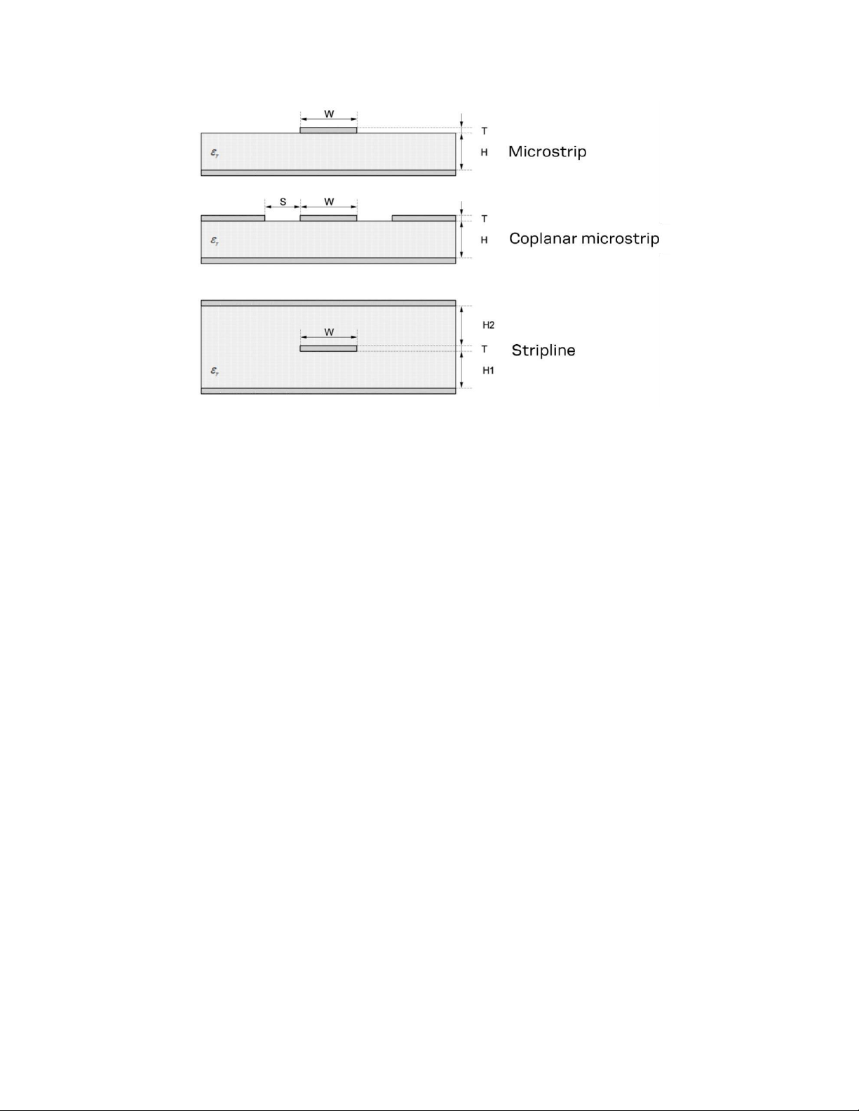
5.2.1 RF Transmission Line Design
RF transmission lines such as the ones from the ANT0 and ANT1 pins up to the related antenna
connectors must be designed so that the characteristic impedance is as close as possible to 50
Ωillustrates the design options and the main parameters to be considered when
implementing a transmission line on a PCB:
•Microstrip: track coupled to a single ground plane, separated by dielectric
material),
•Coplanar microstrip: track coupled to ground plane and side conductors,
separated by dielectric material).
•Stripline: track sandwiched between two parallel ground planes, separated by
dielectric material).
The coplanar microstrip is the most common configuration for a printed circuit board
(PCB).
Document Information Page 11 of 31
FSS JODY-W263 Integration Instructions Rev 02.docx
www.foresightsports.com
Figure 1: Transmission line trace design
To properly design a 50 Ω transmission line, the following remarks should be
considered:
•The designer should provide enough clearance from surrounding traces and
ground in the same layer; in general, a trace to ground clearance of at least two
times the trace width should be considered, and the transmission line should be
“guarded” by ground plane area on each side.
•The characteristic impedance can be calculated as first iteration using tools
provided by the layout software. It is advisable to ask the PCB manufacturer to
provide the final values that are usually calculated using dedicated software and
available stack-ups from production. It could also be possible to request an
impedance coupon on panel’s side to measure the real impedance of the traces.
•FR-4 dielectric material, although its high losses at high frequencies can be
considered in RF designs providing that:
oRF trace length must be minimized to reduce dielectric losses.
oIf traces longer than a few centimeters are needed, it is recommended to use
a coaxial connector and cable to reduce losses.
oStack-up should allow for wide 50 Ωtraces and at least 200 µm trace width is
recommended to assure good impedance control over the PCB
manufacturing process.
oFR-4 material exhibits poor thickness stability and thus less control of
impedance over the trace length. Contact the PCB manufacturer for specific
tolerance of controlled impedance traces.
Document Information Page 12 of 31
FSS JODY-W263 Integration Instructions Rev 02.docx
www.foresightsports.com
•For PCBs using components larger than 0402 and dielectric thickness below 200
µm, it is recommended to add a keep-out (that is, clearance, a void area) on the
ground reference layer below any pin present on the RF transmission lines to
reduce parasitic capacitance to ground.
•The transmission lines width and spacing to GND must be uniform and routed as
smoothly as possible: route RF lines in 45° angle.
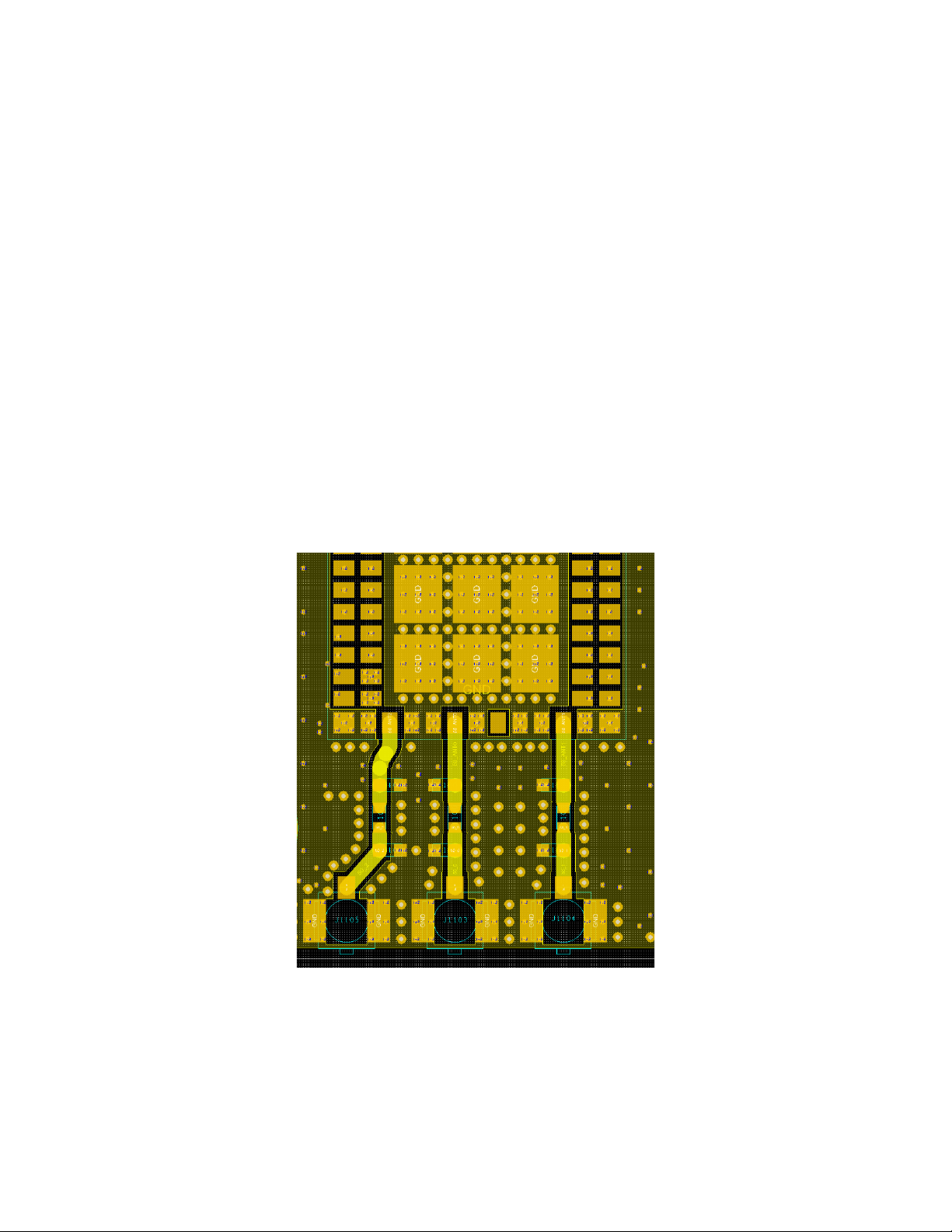
•Add GND stitching vias around transmission lines as shown in Figure 2.
•Ensure solid metal connection of the adjacent metal layer on the PCB stack-up to
main ground layer, providing enough vias on the adjacent metal layer as shown
in Figure 2.
•Route RF transmission lines far from any noise source (as switching supplies and
digital lines) and from any sensitive circuit to avoid crosstalk between RF traces
and Hi-impedance or analog signals.
•Avoid stubs on the transmission lines, any component on the transmission line
should be placed with the connected pin over the trace. Also avoid any
unnecessary component on RF traces.
Figure 2: Example of RF trace and ground design from JODY-W2 EVK

Document Information Page 13 of 31
FSS JODY-W263 Integration Instructions Rev 02.docx
www.foresightsports.com
5.2.2 Antenna Design
Designers must take care of the antennas from all perspective at the very start of the
design phase when the physical dimensions of the application board are under
analysis/decision, since the RF compliance of the device integrating JODY-W2 module
with all the applicable required certification schemes heavily depends on antennas
radiating performance.
•External antennas such as linear monopole:
oExternal antennas basically do not imply physical restriction to the design
of the PCB where the module is mounted.
oThe radiation performance mainly depends on the antennas. It is required
to select antennas with optimal radiating performance in the operating
bands.
oRF cables should be carefully selected with minimum insertion losses.
Additional insertion loss will be introduced by low quality or long cable.
Large insertion loss reduces radiation performance.
oA high quality 50 Ωcoaxial connector provides proper PCB-to-RF-cable
transition.
•Integrated antennas such as patch-like antennas:
oInternal integrated antennas imply physical restriction to the PCB design:
▪Integrated antenna excites RF currents on its counterpoise, typically the
PCB ground plane of the device that becomes part of the antenna; its
dimension defines the minimum frequency that can be radiated.
Therefore, the ground plane can be reduced down to a minimum size
that should be similar to the quarter of the wavelength of the minimum
frequency that has to be radiated, given that the orientation of the
ground plane related to the antenna element must be considered.
▪The RF isolation between antennas in the system must be as high as
possible and the correlation between the 3D radiation patterns of the
two antennas has to be as low as possible.
▪In general, an RF separation of at least a quarter wavelength between
the two antennas is required to achieve a minimum isolation and low
pattern correlation; increased separation should be considered, if
possible, to maximize the performance and fulfil the requirements in
Table 8.

Document Information Page 14 of 31
FSS JODY-W263 Integration Instructions Rev 02.docx
www.foresightsports.com
▪A numerical example for estimating the physical restrictions on a PCB is
given here: Frequency = 2.4 GHz → Wavelength = 12.5 cm → Quarter
wavelength = 3.5 cm
oRadiation performance depends on the whole product and antenna
system design, including product mechanical design and usage. Antennas
should be selected with optimal radiating performance in the operating
bands according to the mechanical specifications of the PCB and the
whole product.
Table 7 summarizes the requirements for the antenna RF interface while Table 8
specifies additional requirements for dual antenna design implementation.
Item
Requirements
Remarks
Impedance
50 Ω nominal characteristic
impedance
The impedance of the antenna RF
connection must match the 50 Ω
impedance of Antenna pins.
Frequency range
2400 - 2500 MHz
5150 - 5850 MHz
For 802.11b/g/n and Bluetooth.
For 802.11a/n/ac.
Return loss
S11 < -10 dB (VSWR < 2:1)
recommended
S11 < -6 dB (VSWR < 3:1)
acceptable
The Return loss or the S11, as the
VSWR, refers to the amount of
reflected power, measuring how
well the primary antenna RF
connection matches the 50 Ω
characteristic impedance of antenna
pins.
The impedance of the antenna
termination must match as much as
possible the 50 Ω nominal
impedance of antenna pins over the
operating frequency range, to
maximize the amount of power
transferred to the antenna.
Efficiency
> -1.5 dB ( > 70% ) recommended
> -3.0 dB ( > 50% ) acceptable
The radiation efficiency is the ratio
of the radiated power to the power
delivered to antenna input: the
efficiency is a measure of how well
an antenna receives or transmits.
Maximum gain
The maximum antenna gain must
not exceed the value specified in
type approval documentation to
comply with regulatory agencies
radiation exposure limits.
Table 7: Summary of antenna interface requirements

Document Information Page 15 of 31
FSS JODY-W263 Integration Instructions Rev 02.docx
www.foresightsports.com
Item
Requirements
Remarks
Isolation
(in-band)
S21 > 30 dB recommended
The antenna-to-antenna isolation is
the S21 parameter between the two
antennas in the band of operation.
Lower isolation might be acceptable
depending on use-case scenario
and performance requirements.
Isolation
(out-of-band)
S21 > 35 dB recommended
S21 > 30 dB acceptable
Out-of-band isolation is evaluated
in the band of the aggressor to
ensure that the transmitting signal
from the other radio is sufficiently
attenuated by the receiving antenna
to avoid saturation and
intermodulation effect at the
receiver’s port.
Table 8: Summary of Wi-Fi/Bluetooth coexistence requirements
⚠In dual antenna configuration, a good isolation is critical to achieve optimal throughput
performance in Wi-Fi/Bluetooth coexistence mode while operating in the same 2.4 GHz band. In
both the cases, while selecting external or internal antennas, observe the following
recommendations:
•Select antennas that provide an optimal return loss (or VSWR) over all operating
frequencies.
•Select antennas that provide optimal efficiency figure over all operating frequencies.
•Select antennas that provide appropriate gain not to exceed the regulatory limits
specified in some countries like the FCC in the United States.
A method to design for antenna micro-strip evaluation is to place an U.FL connector close to the
embedded PCB or chip Antenna. The UFL connector needs only to be mounted on units used for
verification.
5.2.2.1 RF Connector Design
If an external antenna is required, the designer should consider using a proper RF connector. It
is the responsibility of the designer to verify the compatibility between plugs and receptacles
used in the design.
Table 9 suggests some RF connector plugs that can be used by the designers to connect RF
coaxial cables based on the declaration of the respective manufacturers. The Hirose U.FL-R-SMT
RF receptacles (or similar parts) require a suitable mated RF plug from the same connector
series. Due to wide usage of this connector, several manufacturers offer compatible equivalents.

Document Information Page 16 of 31
FSS JODY-W263 Integration Instructions Rev 02.docx
www.foresightsports.com
Manufacturer
Series
Remarks
Hirose
U.FL® Ultra Small Surface Mount
Coaxial Connector
Recommended
I-PEX
MHF® Micro Coaxial Connector
Tyco
UMCC® Ultra-Miniature Coax
Connector
Amphenol RF
AMC® Amphenol Micro Coaxial
Lighthorse Technologies, Inc.
IPX ultra micro-miniature RF
connector
Table 9: U.FL compatible plug connector
Typically, the RF plug is available as a cable assembly. Different types of cable assembly are
available; the user should select the cable assembly best suited to the application. The key
characteristics are:
•RF plug type: select U.FL or equivalent
•Nominal impedance: 50 Ω
•Cable thickness: Typically, from 0.8 mm to 1.37 mm. Thicker cables minimize insertion
loss.
•Cable length: Standard length is typically 100 mm or 200 mm; custom lengths may be
available on request. Select shorter cables to minimize insertion loss.
•RF connector on the other side of the cable: for example, another U.FL (for board-to-
board connection) or SMA (for panel mounting)
SMT connectors are typically rated for a limited number of insertion cycles. In addition, the RF
coaxial cable may be relatively fragile compared to other types of cables. To increase application
ruggedness, connect U.FL connector to a more robust connector such as SMA fixed on panel.
☞A de-facto standard for SMA connectors implies the usage of reverse polarity connectors (RP-
SMA) on end-user accessible Wi-Fi and Bluetooth interfaces to increase the difficulty to replace
the antenna with higher gain versions and exceed regulatory limits.
The following recommendations apply for proper layout of the connector:
•Strictly follow the connector manufacturer’s recommended layout. Some examples are
provided below:
oSMA Pin-Through-Hole connectors require GND keep-out (clearance or void
area) on all the layers around the central pin up to annular pins of the four GND
posts.
oU.FL surface mounted connectors require no conductive traces (that is, clearance,
a void area) in the area below the connector between the GND land pins.
•If the RF pin size on the connector is wider than the microstrip, remove the GND layer
beneath the RF connector to minimize the stray capacitance thus keeping the RF line 50
Ω. For example, the active pin of U.FL connector must have a GND keep-out at least on
the first inner layer to reduce parasitic capacitance to ground.

Document Information Page 17 of 31
FSS JODY-W263 Integration Instructions Rev 02.docx
www.foresightsports.com
5.2.2.2 Integrated Antenna Design
If integrated antennas are used, the transmission line is terminated by the antennas themselves.
Follow the guidelines mentioned below:
•The antenna design process should start together with the mechanical design of the
product. PCB mock-ups are useful in estimating overall efficiency and radiation path of
the intended design during early development stages.
•Use antennas designed by an antenna manufacturer providing the best possible return
loss (or VSWR).
•Provide a ground plane large enough according to the related integrated antenna
requirements. The ground plane of the application PCB may be reduced down to a
minimum size that must be similar to one quarter of wavelength of the minimum
frequency that has to be radiated, however overall antenna efficiency may benefit from
larger ground planes. Proper placement of the antenna and its surroundings is also
critical for antenna performance. Avoid placing the antenna close to conductive or RF-
absorbing parts such as metal objects or ferrite sheets as they may absorb part of the
radiated power, shift the resonant frequency of the antenna or affect the antenna
radiation pattern.
•It is highly recommended to strictly follow the specific guidelines provided by the
antenna manufacturer regarding correct installation and deployment of the antenna
system, including PCB layout and matching circuitry.
•Further to the custom PCB and product restrictions, antennas may require
tuning/matching to reach the target performance. It is recommended to plan
measurement and validation activities with the antenna manufacturer before releasing
the end-product to manufacturing.
•The receiver section may be affected by noise sources like hi-speed digital busses. Avoid
placing the antenna close to busses as DDR or consider taking specific countermeasures
like metal shields or ferrite sheets to reduce the interference.
Take care of interaction between co-located RF systems like LTE sidebands on 2.4 GHz band.
Transmitted power may interact or disturb the performance of JODY-W2 modules where specific
LTE filter is not present.
6 Antenna Reference Design
6.1 Scope
This document defines the essential specifications necessary to implement the JODY-W2
antenna reference designs as used in certification. It is part of the equipment certification
application issued to FCC and ISED. The information contained herein and its references should
be sufficient to guide a skilled person to implement the design on a host carrier. It will provide
the designer with PCB layout details and expected performance specifications.

Document Information Page 18 of 31
FSS JODY-W263 Integration Instructions Rev 02.docx
www.foresightsports.com
This document supports a connector-based design for the use of external antennas (one for
each antenna pin of the module).
6.2 General description and requirements
JODY-W2 series modules provide two RF interfaces for connecting external antennas. The
antenna ports ANT0 and ANT1 have a nominal characteristic impedance of 50 Ω and must be
connected to the related antenna through a 50 Ω transmission line to allow proper impedance
matching along the RF path. A bad termination of the pin may result in poor performance or
even damage the RF section of the module.
For optimal performance in multiradio mode, the isolation between the antennas shall target the
requirements as specified in Table 10 and Table 11 in order to ensure good performance.
Item
Requirements
Remarks
Impedance
50 Ω nominal characteristic
impedance
The impedance of the antenna RF
connection must match the 50 Ω
impedance of the antenna pins.
Frequency range
2400 - 2500 MHz
5150 - 5850 MHz
For 802.11b/g/n and Bluetooth.
For 802.11a/n/ac.
Return loss
S11 < -10 dB (VSWR < 2:1)
recommended
S11 < -6 dB (VSWR < 3:1)
acceptable
The return loss or the S11, as the
VSWR, refers to the amount of
reflected power, measuring how
well the primary antenna RF
connection matches the 50 Ω
characteristic impedance of antenna
pins.
The impedance of the antenna
termination must match as much as
possible the 50 Ωnominal
impedance of antenna pins over the
operating frequency range, to
maximize the amount of power
transferred to the antenna.
Efficiency
> -1.5 dB ( > 70% ) recommended
> -3.0 dB ( > 50% ) acceptable
The radiation efficiency is the ratio
of the radiated power to the power
delivered to antenna input: the
efficiency is a measure of how well
an antenna receives or transmits.
Maximum gain
The maximum antenna gain must
not exceed the value specified in
type approval documentation to
comply with regulatory agencies
radiation exposure limits.
Table 10: Summary of antenna interface requirements
Document Information Page 19 of 31
FSS JODY-W263 Integration Instructions Rev 02.docx
www.foresightsports.com
Item
Requirements
Remarks
Isolation
(in-band)
S21 > 25 dB recommended
S21 > 20 dB acceptable
The antenna to antenna isolation is
the S21 parameter between the two
antennas in the band of operation.
Isolation
(out-of-band)
S21 > 35 dB recommended
S21 > 30 dB acceptable
Out-of-band isolation is evaluated
in the band of the aggressor to
ensure that the transmitting signal
from the other radio is sufficiently
attenuated by the receiving antenna
to avoid saturation and
intermodulation effect at the
receiver’s port.
Envelope correlation
Coefficient (ECC)
ECC < 0.1 recommended
ECC < 0.5 acceptable
The ECC parameter correlates the
far field parameters between
antennas in the same system. A low
ECC parameter is fundamental to
improve performance in MIMO-
based systems.
Table 11: Summary of MIMO and Wi-Fi/Bluetooth coexistence requirements. MIMO is not applicable for
JODY-W2.
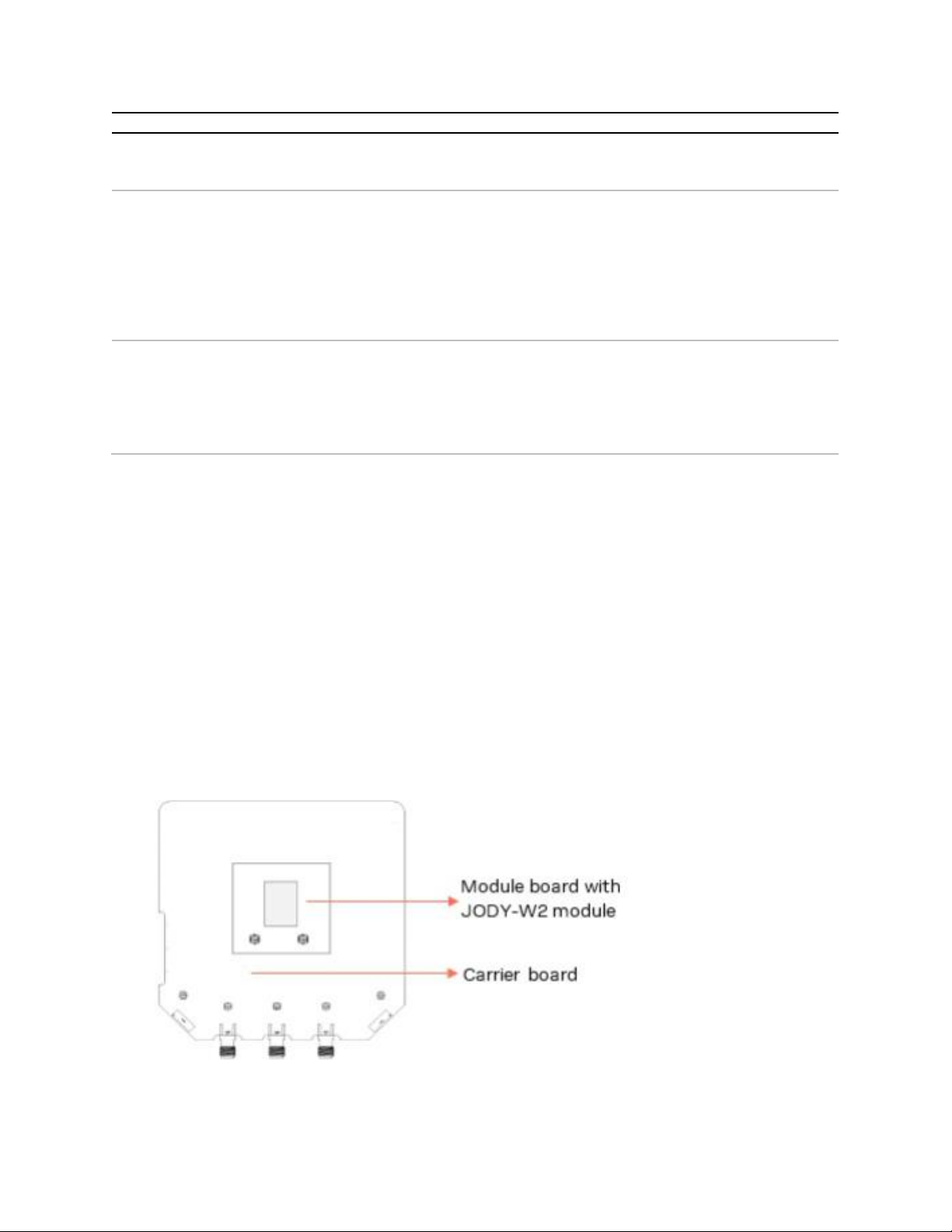
6.3 Reference design of RF path
JODY-W2 is certified with a set-up including JODY-W2 module board with it’s RF paths
connected to the carrier board with RF coaxial cables. The antennas are connected to the carrier
board through SMA connectors. Below are the relevant components listed.
•Module board including U.FL connectors with JODY-W2 mounted.
•Carrier board including U.FL connectors to interface the module board and SMA
connectors to connect antennas.
•Coaxial cables with U.FL connectors connecting the module board’s RF traces to the
carrier board’s RF traces.
•Antennas connected to the carrier board’s SMA connectors.
Figure 3: Definition of Module board and Carrier board
Document Information Page 20 of 31
FSS JODY-W263 Integration Instructions Rev 02.docx
www.foresightsports.com
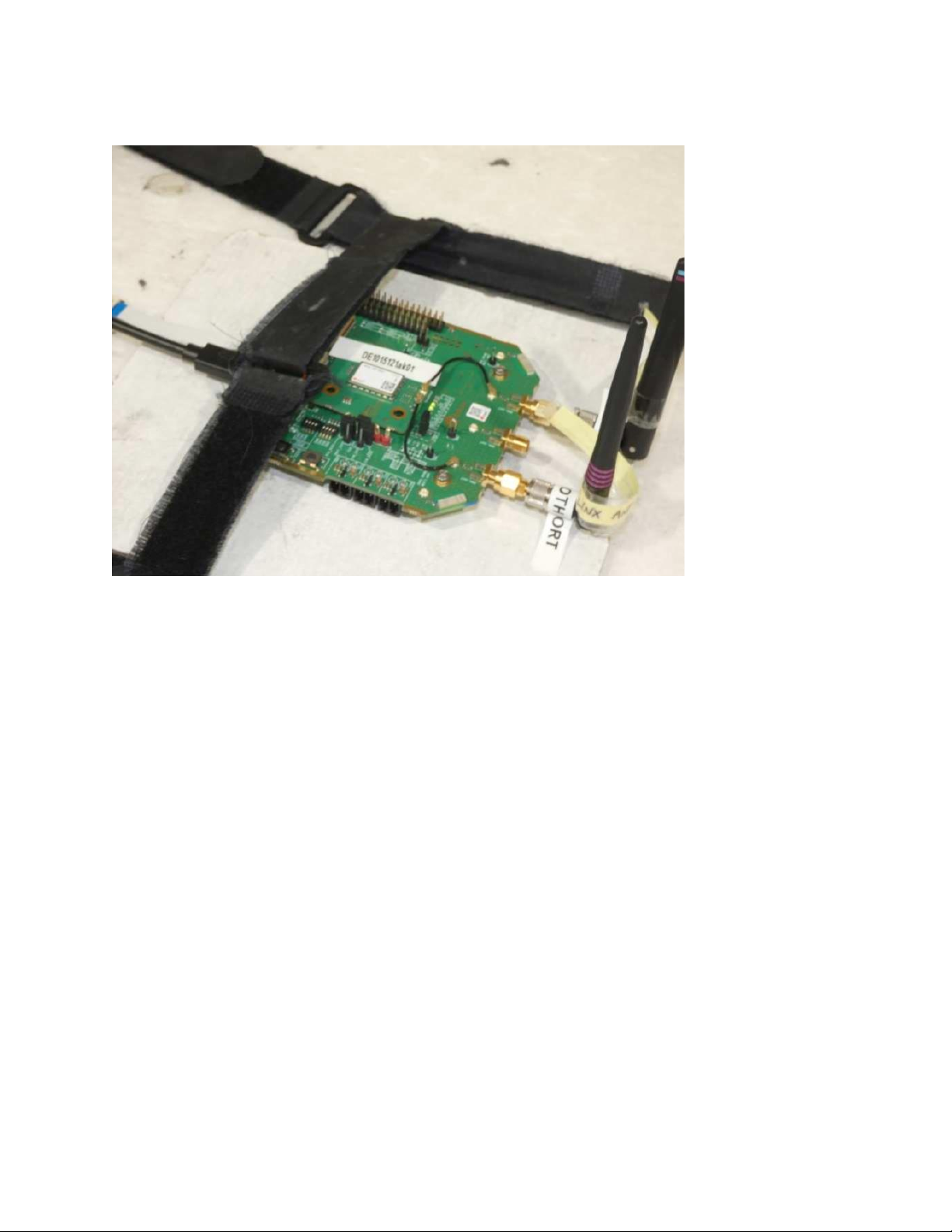
Figure 4: Test set-up
3.1 RF trace PCB routing
The PCB routing connecting the module’s antenna pins to module board U.FL connectors are
designed with coplanar microstrips. Coplanar microstrips are also used on the carrier board
connecting the U.FL connectors with the SMA connectors to which the external antennas or test
equipment are connected. Figure 5 and Table 12 shows the design stack-up including
dimensions of the 50 Ω coplanar microstrips implemented.
Regarding the coplanar microstrips the ground planes beside the signal trace are connected to
the inner layer ground plane using vias. The vias are placed with a maximum distance of 0.5 mm
to the coplanar ground edge and a maximum pitch of 2 mm. The top layer is coated with
generic LPI solder stop mask.
The SMA connectors on the carrier board are used for mounting antennas. For Bluetooth and
Wi-Fi operation in the 2.4 GHz band and Wi-Fi operation in the 5 GHz band, the module has
been tested and approved for use with antennas up to 2 dBi antenna gain.
Table of contents


