Generalmusic P500 User manual

11
11
1 oo
oo
o
CODE:277319
Index&Warnings
Soldering point.
Male connector.
Female connector.
M/F faston connector.
Test point.
Supply voltage.
Logic supply ground.
Analog supply ground.
Signal ground.
Chassis ground.
Flag joined with one or more flags with the same signal name inscribed.
GENERALMUSICS.p.A.SalesDivision:47842S.GiovanniinMarignano(RN)ITALY-ViadelleRose,12-tel.0541/959511-tlx550555GMUSICI-fax0541/957404
Technical Specifications, Test Procedures & Adjustments
2
Notice
Service must be carried out by qualified personnel only. Any tampering carried out by unqualified personnel during the guarantee
period will forfeit the right to guarantee.
For a correct operation of the instrument, after having switched off, be careful to wait at least 3 seconds before switching on again.
To improve the device's specifications, the schematic diagrams may be subject to change without prior notice.
SchematicNotes
All components marked by this symbol have special safety characteristics, when replacing any of these components use only
manufacturer's specified parts.
The (µ) micro symbol of capacitance value is substituted by U. The (Ω) omega symbol of resistance value is substituted by E.
The electrolytic capacitors are 25Vdc rated voltage unless otherwise specified. All resistors are 1/4W unless otherwise specified.
ATTENTION
Observe precautions when handling
electrostatic sensitive devices
SERVICE MANUAL
Schematic Diagrams
Layout
4
Wiring Connections
6
7
Power Amplifier Board
Inputs Board, Supplies & Protections Board
5
8
Display Board & Part List

oo
oo
o 22
22
2
TECHNICAL SPECIFICATIONSTECHNICAL SPECIFICATIONS
TECHNICAL SPECIFICATIONS
Dimensions: (WxHxD) 483x88x325mm (2U)
Weight: 13Kg
Power Requirements: (230Vac±10% 50Hz) 500VA
Output Power: (4Ωstereo/parallel) 2x 300Watts
(8Ωstereo/parallel) 2x 200Watts
(8Ωbridge) 600Watts
(16Ωbridge) 400Watts
Max. Undistorted Out: (4Ωstereo/parallel) 98Vpp
(8Ωstereo/parallel) 113Vpp
(8Ωbridge) 194Vpp
Input Sensitivity: (constant sensitivity) 0.775Vrms (0dB)
(constant gain) 1.75Vrms (+7dB)
Input Impedance: (balanced) 30KΩ
(unbalanced) 15KΩ
Voltage Gain: (constant sensitivity) 33±0.5dB
(constant gain) 26±0.5dB
Slew Rate: 25V/µS
Damping Factor: (4Ωstereo/parallel) >400
(8Ωstereo/parallel) >800
Frequency Response (-0.2dB) 20Hz÷20KHz
at Full Power: (-3dB) 10Hz÷60KHz
IMD: (SMPTE 60Hz/7KHz 4:1) <0.1%
THD: (THD+N) <0.1%
S/N Ratio: (unweighted) >95dB
Crosstalk: (1KHz) >60dB
TEST PROCEDURES & ADJUSTMENTSTEST PROCEDURES & ADJUSTMENTS
TEST PROCEDURES & ADJUSTMENTS
PrecautionPrecaution
Precaution
➭To prevent short circuit during any test, the oscilloscope must bethe oscilloscope must be
the oscilloscope must bethe oscilloscope must be
the oscilloscope must be
EARTH insulatedEARTH insulated
EARTH insulated, this occurs because some test require to connect its
probe to the amplifier output, non-compliance may cause damages to
oscilloscope inputs circuitry.
➭Before removing or installing any modules and connectors, disconnectdisconnect
disconnectdisconnect
disconnect
the amplifier from AC MAINSthe amplifier from AC MAINS
the amplifier from AC MAINS and measure the DC supply voltages
across each of the power suppliy capacitors. If your measurement on any
of the caps is greater than 10Vdc, connect a 100Ω20W resistor across
the applicable caps to discharge them for your safety. Remember to
remove the discharge resistor immediately after discharging caps. Do notDo not
Do notDo not
Do not
power up the amplifier with the discharge resistor connectedpower up the amplifier with the discharge resistor connected
power up the amplifier with the discharge resistor connected.
➭Read these notes entirely before proceeding to any operation. These
notes are not comprehensive of all damages that possibly occur, but
includes some specifically advices, checks and adjustments relative to
this amplifier.
RemarksRemarks
RemarksRemarks
Remarks
➭The power supply utilizes a dual bipolar DC rail configuration with low and
high voltages; one positive and one negative low rail (+/-Vcc1) and one
positive and one negative high rail (+/-Vcc2).
Visual CheckVisual Check
Visual Check
➭Use compressed air to clear dust in the amplifier chassis.
➭Before proceed to supply the amplifier check visually the internal assem-
bly, if appears an evident damage find the most possible reasons that
cause it.
➭Check the wiring cables for possible interruptions or shorts.
➭If the damage has burnt a printed circuit board don’t try to repair it, re-
place with a new one.
Test InstrumentsTest Instruments
Test Instruments
➭Audio Generator
➭Dual Trace Oscilloscope
➭Digital Multimeter
➭2Ω1000W, 4Ω500W, 100Ω20W resistors
➭Variac (0÷250Vac)
➭Temperature Meter
SetupSetup
SetupSetup
Setup
➭Connect the Variac between the mains and the amplifier and set it at zero
voltage.
➭Set the amplifier in STEREO MODE and turn full clockwise the LEVEL
potentiometers.
➭Connect the audio generator to the channel inputs and set it to 1KHz
775mVRMS (0dB) sinusoidal signal.
➭Insert the temperature meter through the IC3 interstice located at centre
of heatsink.
➭The procedures that follow must be executed subsequently in the order
specified.
Supply CheckSupply Check
Supply Check
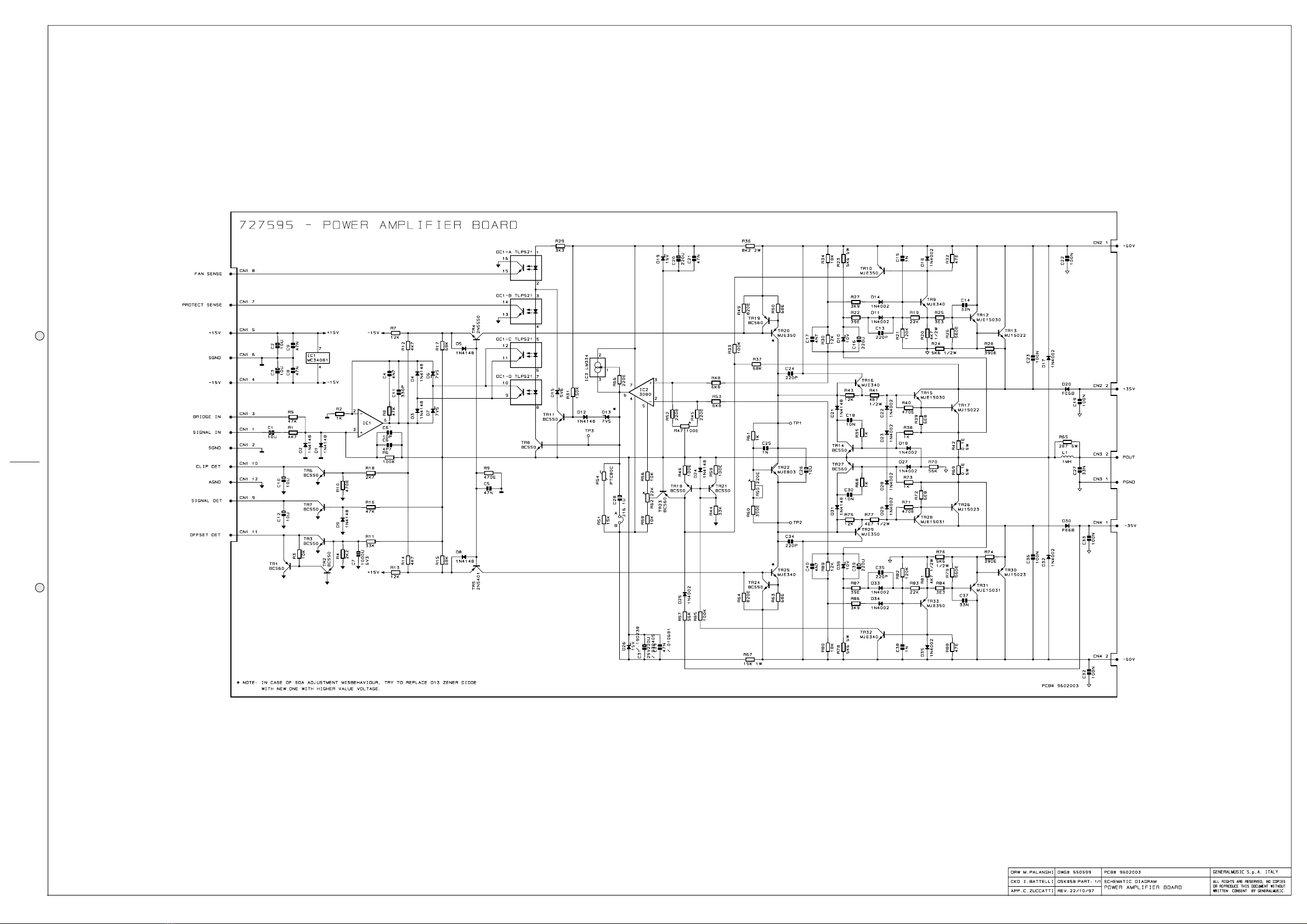
➭Remove the transformer secondary fuses (located on SUPPLY & PRO-
TECTIONS board), set the Variac to the nominal mains voltage, check
with the Multimeter the AC supply voltages:
F1-F2=52±2Vac F3-F4=90±3Vac.
➭Re-set the Variac at zero voltage, turn off the amplifier and put the fuses
back on its holders.
➭Connect the oscilloscope probes CH1/2 to the channel outputs, before
RL1 and RL2, set both to 20V/div. 200µS/div.
➭Set up the Variac slowly monitoring the Outputs with the oscilloscope
CH1/2 connected, it should display the sinusoidal input signal amplified
with no distortions, if a distortion occur check the POWER AMPLIFIER
boards as suggested in the ADVICES section.
➭If the protection trips, turn off the amplifier, wait some minutes and
disconnect the supplies from the outputs modules (CN2, CN3 on POWER
AMPLIFIER boards), continue to check the supplies.
➭CAUTION: Before re-connecting the output modules to the supplies,CAUTION: Before re-connecting the output modules to the supplies,
CAUTION: Before re-connecting the output modules to the supplies,CAUTION: Before re-connecting the output modules to the supplies,
CAUTION: Before re-connecting the output modules to the supplies,
you must have the capacitors discharged for your safety: connect ayou must have the capacitors discharged for your safety: connect a
you must have the capacitors discharged for your safety: connect a
100100
100100
100ΩΩ
ΩΩ
Ω20W resistor across the caps and remove the resistor just after20W resistor across the caps and remove the resistor just after
20W resistor across the caps and remove the resistor just after20W resistor across the caps and remove the resistor just after
20W resistor across the caps and remove the resistor just after
they are discharged.they are discharged.
they are discharged.
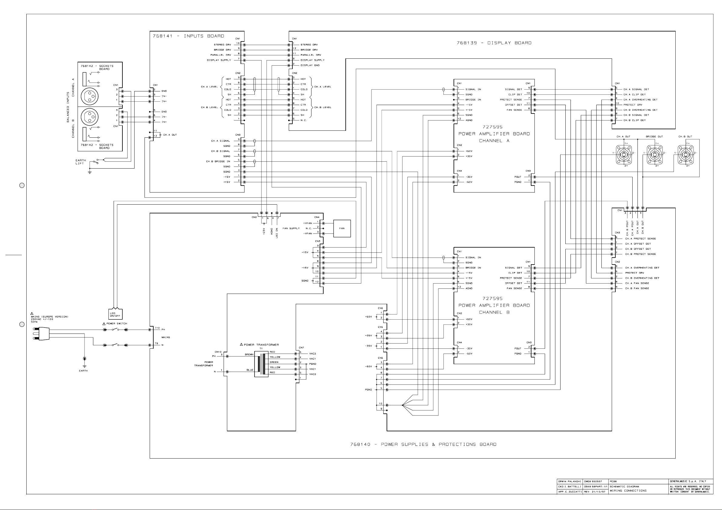
➭Finally verify the DC supplies on SUPPLIES & PROTECTIONS Board:
T8 (+Vcc2) =+61±2Vdc
T5 (+Vcc1) =+35±1.5Vdc
T6 (-Vcc1) =-35±1.5Vdc
T7 (-Vcc2) =-61±2Vdc
CN2 pin1 =+23±1Vdc
CN3 pin3-4-5 =+15±1Vdc
CN3 pin8-9-10 =-15±1Vdc
➭If one or more voltages don’t correspond, check the rectifiers, capacitors
and transformers disconnecting them from circuitry, refer to schematics.
Channels CheckChannels Check
Channels Check
➭The channel A is facing the front and channel B the rear of the chassis.
➭These procedures are intended for one channel at a time, repeat these
operation for the other channel.
➭Verify, with the Multimeter, the insulation between the heatsink and the
transistors collectors.
➭SETUP:SETUP:
SETUP:SETUP:
SETUP:
Connect the CH1 scope GND clip to CN3 pin 1 (GND terminal).
Connect the CH1 probe tip to CN3 pin 2 (AMP output).
Connect the CH2 probe tip to D20 cathode.
Set the LEVEL potentiometers full clockwise.
The load resistor is disconnected.
➭INITIAL TEST:INITIAL TEST:
INITIAL TEST:INITIAL TEST:
INITIAL TEST:
Increase slowly the Variac. The channel output signals must be symmetri-
cal respect the GND without visible distortion and oscillation as shown in
Fig.1 Trace A
. If there is a distortion read the section ADVICES and
proceed to check the other channel.
Verify that, when the heatsink temperature is less than 50°c, the cooling
fan voltage must be between 10 and 14Vdc.
➭HIGH RAIL CHECK:HIGH RAIL CHECK:
HIGH RAIL CHECK:HIGH RAIL CHECK:
HIGH RAIL CHECK:
When the output signal (Positive half-wave) is less than 30Vp the voltage
on D20 cathode must remain constant at 36V, when the output signal
exceeds 30Vp the voltage must follow the output signal with 6V offset
(see
Fig.1 Trace B
), to check the negative high rail connect the probe to
D30 anode (see
Fig.1 Trace C
).
Connect the 4Ω500W load on the output and repeat the INITIAL and
HIGH RAIL checks.
Check the signal clipping, it must occur at 48±2Vpp (see
Fig.2 Trace
A,B,C
).
Fig. 1Fig. 1
Fig. 1Fig. 1
Fig. 1 Trace B (20V/div.)
Trace A (20V/div.)
Trace C (20V/div.)

33
33
3 oo
oo
o
Verify the voltages across the diodes D19 and D26; they must be 14.8
±0.5Vdc.
➭SIGNAL/CLIP SENSOR CHECK:SIGNAL/CLIP SENSOR CHECK:
SIGNAL/CLIP SENSOR CHECK:SIGNAL/CLIP SENSOR CHECK:
SIGNAL/CLIP SENSOR CHECK:
Set the LEVEL pot to minimum, set the scope timebase at 1V/div. 200µS/
div., then increase the level and check the SIGNAL/CLIP led activity: it
must turn on (green light) when the amplifier output is higher than 1Vp.
Set the scope at 20V/div. and increase the level, check the led: it must
change from green to red colour at the amplifier output signal clipping.
➭CURRENT AND SHORT CIRCUIT SENSOR CHECK:CURRENT AND SHORT CIRCUIT SENSOR CHECK:
CURRENT AND SHORT CIRCUIT SENSOR CHECK:CURRENT AND SHORT CIRCUIT SENSOR CHECK:
CURRENT AND SHORT CIRCUIT SENSOR CHECK:
Set the CH2 sensitivity to 0.5V/div., connect the scope CH1, GND clip at
CN3 pin 2 (AMP output) and the probe tip at TR26 (PNP) emitter, con-
nect the CH2 probe tip at TR17 (NPN) emitter.
Set the generator to have approx. 1Vp on the emitters: their difference
must be less than 0.2V on the peaks (see
Fig.3 Trace A & B
).
Connect a 2Ω1000W load. Increase the input signal, the output current
limiter must keep the emitter voltages (both half channel) at 1.25Vp
approx. (see
Fig.4 Trace A
).
Temporarily short the amplifier output: the current limiter must keep the
emitter voltages (both half channel) at 0.8±0.1Vp (see
Fig.4 Trace B
).
➭COOLING FAN & PROTECTION CHECK:COOLING FAN & PROTECTION CHECK:
COOLING FAN & PROTECTION CHECK:COOLING FAN & PROTECTION CHECK:
COOLING FAN & PROTECTION CHECK:
Short circuit pins 15 and 16 of OC1, the fan must run at max. speed
(20÷23Vdc on its tips).
Short circuit pins 13 and 14 of OC1, the PROTECT led must turn on
immediately, the fan must run at max. speed. The PROTECT led of the
other channel must also turn on after 2 Sec. and the relays must discon-
nect the output sockets.
Remove the short circuit, after 3 Sec. both PROTECT leds must turn off
and the relays must re-connect the output sockets.
Temporarily short the emitter and the collector of TR1 the PROTECT led
must turn on and the relays must disconnect the output sockets.
Turn off the amplifier and wait a minute to let the supply caps discharge.
➭OFFSET SENSOR CHECK:OFFSET SENSOR CHECK:
OFFSET SENSOR CHECK:OFFSET SENSOR CHECK:
OFFSET SENSOR CHECK:
Set the Variac to zero voltage output, disconnect the amplifier load and
the supply connection to the Power board (CN2,3,4), turn on the ampli-
fier, connect temporarily (by means of a suitable conductor wire) CN3 pin
2 to +15Vdc (CN1 pin 5), the PROTECT led must turn on in 5 seconds
approx.; the fan must run at maximum speed).
Remove the connection, wait until the leds turn off and after some sec-
onds repeat the check with -15Vdc (available on CN1 pin 4), the led
PROTECT must turn on again.
➭SOA ADJUSTMENT:SOA ADJUSTMENT:
SOA ADJUSTMENT:SOA ADJUSTMENT:
SOA ADJUSTMENT:
Set the scope sensitivity at 5V/div. (both channels).
Disconnect the fan and cut the pins A-B of J16.
Connect the 4Ω500W load and connect the CH2 probe tip at TR23
collector, check the waveform as shown in
Fig 5 Trace B
,
Trace A
show
CH1 that is also connected at TR26 (PNP) emitter.
Set the scope CH2 sensitivity at 2V/div. and connect the probe tip at the
testpoint TP3.
Set the load at 2Ω,wait until the temperature reaches 80°C; then change
the load back to 4Ω.
Adjust the generator level to have the CH1 waveshape as shown in
Fig 6
Trace A
.
Turn the R47 trimmer to level the peaks of the CH2 waveshape as shown
Fig 6 Trace b
.
Solder the pins A-B of J16: the CH2 trace becomes continuous.
Increase the generator level for the max. displacement of the CH2 trace
toward the centre of the screen
Fig 7 Trace b
.
Wait until the temperature reaches 88°C, then turn clockwise the R62
trimmer to activate the SOA control (that is displayed by CH1 trace when
its peak voltage decrease
Fig 7 Trace A
), after some seconds, the chan-
nel goes in PROTECT mode.
Set the CH2 sensitivity at 5V/div. then, with its tip, check the voltage on
D19 cathode: it must be 14V or more.
Activate the fan and check its supply voltage: it must be 20V or more
(max. speed).
Fig. 2Fig. 2
Fig. 2Fig. 2
Fig. 2
Fig. 3Fig. 3
Fig. 3Fig. 3
Fig. 3 Trace A (0.5V/div.)
Trace B (0.5V/div.)
Fig. 5Fig. 5
Fig. 5Fig. 5
Fig. 5
Trace A (5V/div.)
Trace B (5V/div.)
Fig. 4Fig. 4
Fig. 4Fig. 4
Fig. 4 Trace A (0.5V/div.)
Trace B (0.5V/div.)
➭BIAS ADJUSTMENT:BIAS ADJUSTMENT:
BIAS ADJUSTMENT:BIAS ADJUSTMENT:
BIAS ADJUSTMENT:
Remove the CH2 probe, connect CH1 GND clip to CN3 pin 1 (GND
terminal) and its probe tip to CN3 pin 2 (AMP output) and set its sensitiv-
ity at 1V/div.
Set the generator level at zero, connect the Multimeter across
the emit-
ters of TR17 and TR26, when the heatsink temperature reaches 55°C,
turn off the cooling fan and adjust R55 trimmer to read 6±0.5mV.
Adjust the generator level until the sinewave appears at full screen ampli-
tude, No crossover distortion must be detectable: if necessary re-adjust
R55. Re-connect the fan.
➭BANDWIDTH CHECK:BANDWIDTH CHECK:
BANDWIDTH CHECK:BANDWIDTH CHECK:
BANDWIDTH CHECK:
Sweep the generator frequency from 20Hz to 20KHz, the output level
must have not detectable level changes.
➭SLEW RATE CHECK:SLEW RATE CHECK:
SLEW RATE CHECK:SLEW RATE CHECK:
SLEW RATE CHECK:
Set the scope sensitivity to 10V/div. 1µS/div. and set the generator to
1KHz square wave mode. Check the output square wave rising and falling
edge slopes: both must be 10V/µS or more as shown in
Fig 8
.
Inputs Board CheckInputs Board Check
Inputs Board Check
➭These procedures are intended for one channel at a time, repeat these
operations for the other channel.
➭SETUP:SETUP:
SETUP:SETUP:
SETUP:
Connect the CH1 probe to amplifier input of the channel under test and
set both at 500mV/div. 200mS/div.
Connect the CH2 probe to amplifier output of the channel under test and
set it at 10mV/div. 200mS/div.
Set the audio generator at 1KHz sinus. 775mVRMS (0dB).
Set the LEVEL potentiometers full clockwise.
The load resistor is disconnected.
➭CMRR ADJUSTMENTCMRR ADJUSTMENT
CMRR ADJUSTMENTCMRR ADJUSTMENT
CMRR ADJUSTMENT
Temporarily disconnect pin 3 from pin 1 and short the pin 2 (positive
input) and pin 3 (negative input) of XLR input socket.
Adjust the trimmer R10 (channel A) or R21 (channel B) to obtain the
minimum output level.
Fig. 6Fig. 6
Fig. 6Fig. 6
Fig. 6
Trace A (5V/div.)
Trace B (2V/div.)
Fig. 8Fig. 8
Fig. 8Fig. 8
Fig. 8
Trace A (10V/div.)
Fig. 7Fig. 7
Fig. 7Fig. 7
Fig. 7
Trace A (5V/div.)
Trace B (2V/div.)
Trace B (20V/div.)
Trace A (20V/div.)
Trace C (20V/div.)

oo
oo
o 44
44
4
➭GAIN ADJUSTMENTGAIN ADJUSTMENT
GAIN ADJUSTMENTGAIN ADJUSTMENT
GAIN ADJUSTMENT
Re-set the input signal at pin 2 (positive input) and pin 3 (negative input)
short with pin 1 (GND) of XLR input socket.
Set CH2 scope at 500mV/div. and connect it to the output of INPUTS
board (CN3 pin9 for channel A or CN3 pin7 for channel B).
Set the input SENSITIVITY (SW1) at 1.75Vrms, adjust the trimmer R5
(channel. A) or R17 (channel B) to obtain the same amplitude of the
scope signals.
➭AMPLIFIER GAIN CHECKAMPLIFIER GAIN CHECK
AMPLIFIER GAIN CHECKAMPLIFIER GAIN CHECK
AMPLIFIER GAIN CHECK
Set CH2 scope at 20V/div. and connect it to the amplifier output of the
channel under test. By means of the SENSITIVITY switch check the
output levels: at 775mV position the output voltage must be 50±1.5Vp
and at 1.75V position must be 22.5±0.5Vp.
➭AMPLIFIER BRIDGE MODE CHECKAMPLIFIER BRIDGE MODE CHECK
AMPLIFIER BRIDGE MODE CHECKAMPLIFIER BRIDGE MODE CHECK
AMPLIFIER BRIDGE MODE CHECK
Set the amplifier in BRIDGE mode (input signal to channel A), connect
the CH2 probe to the bridge output: the output voltage must be 97±3Vp.
➭SIGNAL TO NOISE RATIO CHECKSIGNAL TO NOISE RATIO CHECK
SIGNAL TO NOISE RATIO CHECKSIGNAL TO NOISE RATIO CHECK
SIGNAL TO NOISE RATIO CHECK
Disconnect the audio generator and short the input (pin 1,2,3 of XLR
socket shorted) the output signal (noise) must be less 1mV.
AdvicesAdvices
AdvicesAdvices
Advices
➭Check the channels one at time to determine which is right (note: if you
have a spare amplifier module that you know as right, use it).
➭If you have determinate that the problem is a short on a rail, you must
check the output transistors.
To determine which transistor devices are bad, use a soldering iron to lift
one leg of each emitter pin and measure the emitter-collector resistance
on each device. Unsolder and lift one leg of each base pin and check the
base-collector resistance of each transistor and replace any that measure
as a short.
If all the transistors are OK, unsolder and lift one leg of each diode and
check them.
Check the circuit board for open foil traces.
Use the Multimeter as Ohm-meter to check the resistors, particularly the
base and emitter resistors of damaged transistor.
➭If the input sinewave appears to be distorted during the negative cycle,
you can assume that the problem is located somewhere in the circuitry of
the positive low rail.
If the positive cycle appears distorted, you can assume that the problem
is in the circuitry of the negative low rail.
➭If the high rails appear distorted or are not modulating as shown in figure,
then the problem probably exists somewhere in the circuitry of the respec-
tive (+ or -) defective high rail. Refer to the schematics.
CH. B CH. A
MIN. LOAD 4
WARNING !
RISK OF HAZARDOUS ENERGY
MAKE PROPER SPEAKERS CONNECTIONS
REFER TO OWNER'S MANUAL BEFORE USING
OUTPUTS
HOT
COLD
GND
WIRING
SENSITIVITY
1.75 V
0.775 V
EARTH
MODE
BRIDGE
P
A
R
A
L
L
E
L
S
T
E
R
E
O
BALANCED BALANCED
CH. B CH. A
INPUTS
AC
~
21 3
AC~
SER.
MOD.
MADE
IN
INDIA
BRIDGE
MIN. LOAD 8 MIN. LOAD 4
PIN 1
PIN 1
+
P500
PROFESSIONAL
POWER AMPLIFIER
by
DESIGNED AND
ENGINEERED IN ITALY
AVIS:
RISQUE DE CHOC ELECTRIQUE-NE PAS OUVRIR
RISK OF ELECTRIC SHOCK
DO NOT OPEN
CAUTION
"WARNING"
TO REDUCE THE
RISK OF FIRE OR ELECTRIC SHOCK
DO NOT EXPOSE THIS PRODUCT TO
PROTECT PROTECT
SIGN/CLIP SIGN/CLIP
BRIDGESTEREO PARALLEL
AB
P500
PROFESSIONAL POWER AMPLIFIER
POWER
ON

55
55
5 oo
oo
o

oo
oo
o 66
66
6

77
77
7 oo
oo
o

oo
oo
o 88
88
8
Spare Part ListSpare Part List
Spare Part List
Code Ref. Description
AccessoriesAccessories
Accessories
277317 Owner’s Manual P-Series
AssemblyAssembly
AssemblyAssembly
Assembly
667644 MSSDCR01 Cover
667643 MSSDCQ01 Chassis
667642 MSSEBB01 Front Panel
667335 MEAYA104 Rear Spacer
657232 HRDKBH51 Level Knob
340048 Cord Lock
238083 FIN27341 Transformer 500W 230Vac
177542 MEATA102 Handle
141200 CONJK351 Speakon Socket
130285 Mains Cable (EU)
110294 Slider Switch (Earth Lift)
110291 SWTPR141 Power Switch
080607 KBPC25 25A 200V Rectifier Diode Bridge
778124 FIN27361 Cables Assembly
Inputs AssembliesInputs Assemblies
Inputs Assemblies
768142768142
768142768142
768142 FIN27305FIN27305
FIN27305FIN27305
FIN27305 Sockets Board (Pcb#9603014)Sockets Board (Pcb#9603014)
Sockets Board (Pcb#9603014)Sockets Board (Pcb#9603014)
Sockets Board (Pcb#9603014)
140228 CONJK151 *Horizontal Jack Stereo Socket
CONJK141 *XLR Female Socket
768141768141
768141768141
768141 FIN27302FIN27302
FIN27302FIN27302
FIN27302 Inputs Board (Pcb#9602004)Inputs Board (Pcb#9602004)
Inputs Board (Pcb#9602004)Inputs Board (Pcb#9602004)
Inputs Board (Pcb#9602004)
110293 *2sw 2pos Slider Switch
110255 *6sw 3pos Vertical Slider Switch
100061 *TL072 Dual J-Fet Operational Amplifier (replace BA4560 for
service)
070245 *100K 20% Vertical Linear Trimmer
070125 *1K 20% Vertical Linear Trimmer
042625 *15K0 1/4W 1% Metalized Film Resistor
042537 *3K01 1/4w 1% Metalized Film Resistor
030085 *2u2 50V 20% Vert Electrolytic Bipolar Capacitor
Display AssembliesDisplay Assemblies
Display Assemblies
768144768144
768144768144
768144 FIN27306FIN27306
FIN27306FIN27306
FIN27306 Led On/Off Board (Pcb#9610036)Led On/Off Board (Pcb#9610036)
Led On/Off Board (Pcb#9610036)Led On/Off Board (Pcb#9610036)
Led On/Off Board (Pcb#9610036)
768139768139
768139768139
768139 FIN27304FIN27304
FIN27304FIN27304
FIN27304 Display Board (Pcb#9610036)Display Board (Pcb#9610036)
Display Board (Pcb#9610036)Display Board (Pcb#9610036)
Display Board (Pcb#9610036)
090194 *BC560 TO92 LN Pnp Transistor
080742 *Led 3mm Wide Diffused Red-Grn
080710 *Led 3mm 60deg Diffused Yel
080705 *Led 3mm 60deg Diffused Red
074561 RESVRD01 *4K7 Linear Rotary Potentiometer
Supplies & Protections AssemblySupplies & Protections Assembly
Supplies & Protections Assembly
768140768140
768140768140
768140 FIN27303FIN27303
FIN27303FIN27303
FIN27303 Power Supplies & Protections Board (Pcb#9602002)Power Supplies & Protections Board (Pcb#9602002)
Power Supplies & Protections Board (Pcb#9602002)Power Supplies & Protections Board (Pcb#9602002)
Power Supplies & Protections Board (Pcb#9602002)
110307 *Relay 24V / 2 Switch 5A 250V
110030 *T10A Fuse 5x20mm (EU)
110023 *T8A Fuse 5x20mm (EU)
110018 *T6.3A Fuse 5x20mm (EU)
090920 *MJE802 TO126 Npn Darl Transistor
090559 *TIP122 TO220 Npn Darlington Transistor
090558 *TIP127 TO220 Pnp Darlington Transistor
090194 *BC560 TO92 LN Pnp Transistor
090183 *BC550 TO92 LN Npn Transistor
080322 *24V 1W 5% Zener Diode
080293 *15V 1W 5% Zener Diode
080282 *13V 1W 5% Zener Diode
080156 *1N4002 1A 100V Rectifier Diode
080103 *1N4148 100mA 75V Signal Diode
060475 *680E 2W 10% Resistor
030891 CAPELJ81 *10000u 63V -10+50% Vert Electrolytic Capacitor FS
030888 *10000u 80v -10+50% V Electrolytic Capacitor FS
020493 *100n 250Vac MKP EMI Capacitor “Siemens”
Power Channels AssemblyPower Channels Assembly
Power Channels Assembly
727588727588
727588727588
727588 FIN27311FIN27311
FIN27311FIN27311
FIN27311 Dual Power Amplifier Board (Pcb#9602003)Dual Power Amplifier Board (Pcb#9602003)
Dual Power Amplifier Board (Pcb#9602003)Dual Power Amplifier Board (Pcb#9602003)
Dual Power Amplifier Board (Pcb#9602003)
727595727595
727595727595
727595 **
**
*Power Amplifier Board (Pcb#9602003) with HeatsinkPower Amplifier Board (Pcb#9602003) with Heatsink
Power Amplifier Board (Pcb#9602003) with HeatsinkPower Amplifier Board (Pcb#9602003) with Heatsink
Power Amplifier Board (Pcb#9602003) with Heatsink
768143768143
768143768143
768143 ****
****
** Power Amplifier Board (Pcb#9602003) without HeatsinkPower Amplifier Board (Pcb#9602003) without Heatsink
Power Amplifier Board (Pcb#9602003) without HeatsinkPower Amplifier Board (Pcb#9602003) without Heatsink
Power Amplifier Board (Pcb#9602003) without Heatsink
230557 *** 1uh Horizontal Coil For Amplifier
100931 *** MC34081 Single J-Fet Operational Amplifier
100928 *** TLP521-4 Quad Optocoupler
100004 *** LM3080 Operational Transconductance Amp.
090917 *** MJE350 TO126 Pnp Transistor
090916 *** MJE340 TO126 Npn Transistor
090201 *** 2N5401 TO92 Pnp Transistor
090200 *** 2N5550 TO92 Npn Transistor
090194 *** BC560 TO92 LN Pnp Transistor
090183 *** BC550 TO92 LN Npn Transistor
080293 *** 15V 1W 5% Zener Diode
080261 *** 10V 1W 5% Zener Diode
080245 *** 7V5 1W 5% Zener Diode
080241 *** 5V6 1W 5% Zener Diode
080171 *** FE6B 6A 100V Fast Recovery Diode
080156 *** 1N4002 1A 100V Rectifier Diode
080103 *** 1N4148 100mA 75V Signal Diode
070207 *** 22K 20% Vertical Linear Trimmer
070084 *** 220E 20% Vertical Linear Trimmer
070065 *** 100E 20% Vertical Linear Trimmer
060620 *** 15K 1W 5% Resistor
060591 *** 8K2 2W 10% Resistor
060571 *** 5K6 2W 10% Resistor
060174 *** 2E7 5W 10% Wire Resistor
060033 *** 0E1 5W 5% Wire Resistor
030715 *** 1000u 6v3 20% Vert Electrolytic Capacitor
030247 *** 10u 25V 20% Vert Electrolytic Bipolar Capacitor
340752 ** TO3 Mica Washer
340750 ** TO126 Mica Washer
340079 ** TO220 Mica Washer
340078 ** TO220 Insulated Bush
140626 ** TO3 Socket
100925 SMCIC831 ** LM334 Adjustable Current Source TO92
090920 SMCTR981 ** MJE802 TO126 Npn Darl Transistor
090919 SMCTRA01 ** MJE15031 TO220 Pnp Transistor
090918 SMCTR991 ** MJE15030 TO220 Npn Transistor
090917 SMCTRA11 ** MJE350 TO126 Pnp Transistor
090916 SMCTR951 ** MJE340 TO126 Npn Transistor
090910 SMCTR961 ** MJ15023A TO3 Pnp Transistor
090907 SMCTR971 ** MJ15022A TO3 Npn Transistor
080820 SMCTH111 ** Ptc 80 PTH59F04BF222TS
110359 FANDC051 *Fan 24Vdc 80x25mm
Note:Note:
Note:Note:
Note:
Each spare part is single quantity unless otherwise specified.
Asterisk prefix explanation:
Omitted = First level spare part.
One asterisk = Second level, part of previous listed first level part.
Two asterisk = Third level, part of previous listed second level part.
Three asterisk = ............
Any request for not above mentioned part must encompass specific description including:
1) Model name,
2) Section name,
3) Module code,
4) Reference name,
5) Quantity number.
Table of contents
Other Generalmusic Amplifier manuals