EB-GS2972
Evaluation Board User Guide
50283 - 2 May 2012
6 of 22
NOTE: Some signals are active LOW so that you will need to switch the bit OFF to
activate the signal.
Refer to the GS2972 Data Sheet for definitions of each bit.
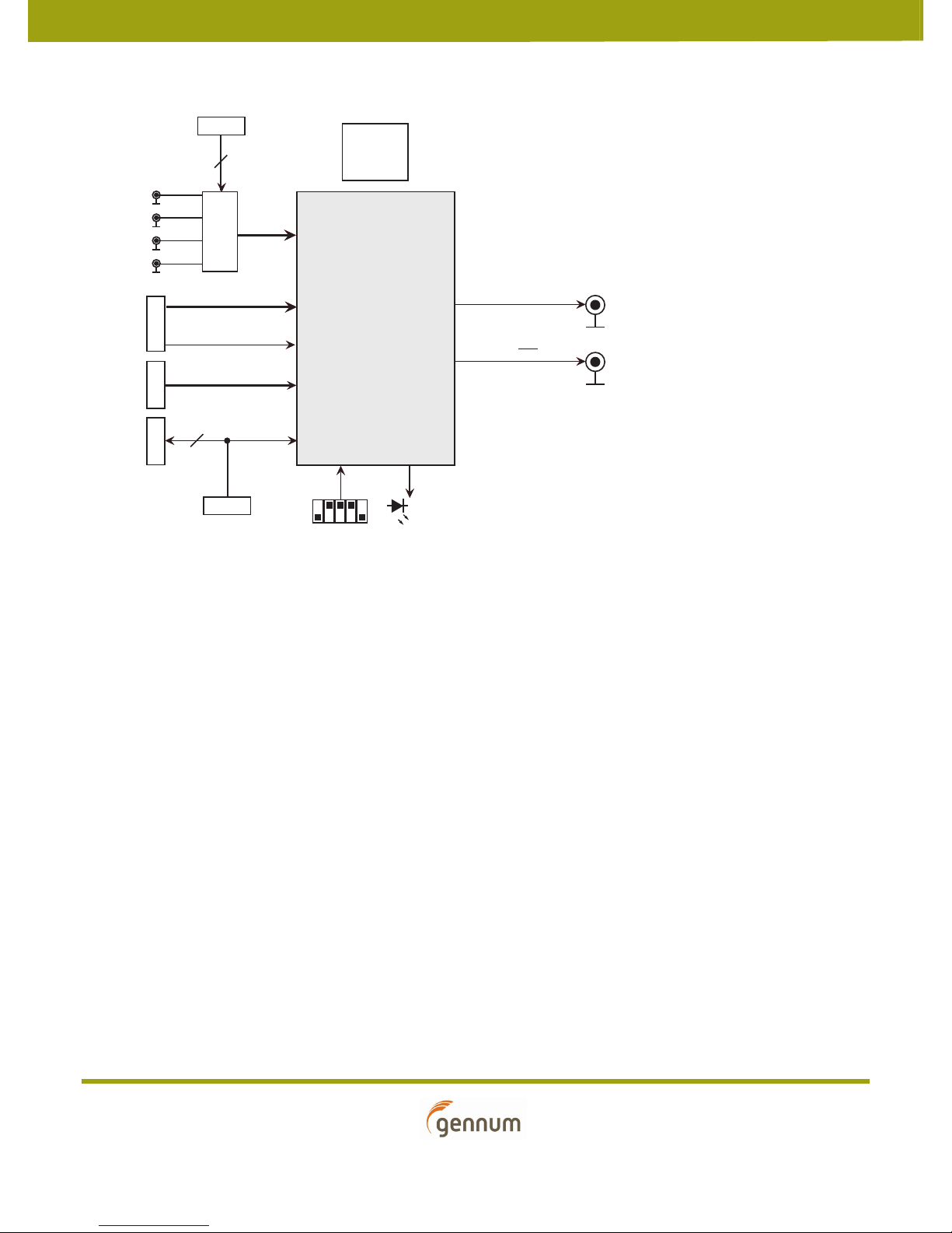
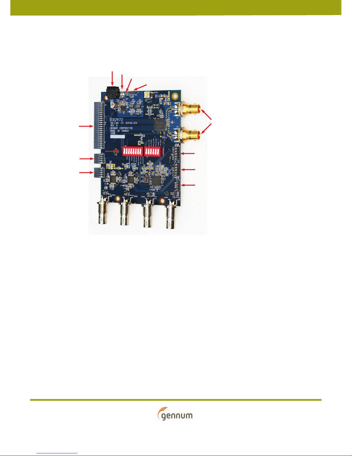
Table 1-1: SW6 and SW7 Settings
Bit Name Description
TIM861
(SW6)
Connected to the GS2972 TIM_861 pin. Used to select external CEA-861 timing mode.
When DETECT_TRSis LOW and TIM-861 is LOW, the device extracts all internal timing from the supplied H:V:F
timing signals. When DETECT_TRSis LOW and TIM-861 is HIGH, the device extracts all internal timing from the
supplied HSYNC, VSYNC, DE timing signals.
When DETECT_TRSis HIGH, the device extracts all internal timing from TRSsignals embedded in the supplied
video stream.
SMPTE_BYPASSn
(SW6)
Connected to the GS2972 SMPTE_BYPASS pin. Used to enable/disable all forms of encoding/decoding,
scrambling and EDH insertion.
When set LOW, the device operates in Data Through mode (DVB_ASI= LOW), or in DVB_ASI mode (DVB_ASI =
HIGH). No SMPTE scrambling takes place and none of the I/O processing features of the device are available
when SMPTE_BYPASS is set LOW.
When set HIGH, the device carries out SMPTE scrambling and I/O processing.
DVB_ASI
(SW6)
Connected to the GS2972 DVB_ASI pin. Used to enable/disable the DVB-ASI data transmission.
When set HIGH, the device will carry out DVB_ASI, word-alignment, I/O processing and transmission. The
SMPTE_BYPASS pin must be set LOW.
When SMPTE_BYPASS and DVB_ASI are both set LOW, the device operates in data-through mode.
RATE_SEL0,
RATE_SEL1
(SW6)
Connected to the GS2972 RATE_SEL0 and RATE_SEL1 pins. Used to configure the operating data rate.
IOPROC_EN/DISn
(SW6)
Connected to the GS2972 IOPROC_EN/DISpin. When IOPROC_EN/DISis HIGH, the I/O processing features of the
device are enabled. When IOPROC_EN/DISis LOW, the I/O processing features of the device are disabled. Only
applicable in SMPTE mode.
20bit/10bitn
(SW6)
Connected to the GS2972 20bit/10bit pin. Used to select the input bus width.
SDO_EN/DISn
(SW6)
Connected to the GS2972 SDO_EN/DISpin. Used to enable or disable the serial digital output stage.
When SDO_EN/DISis LOW, the serial digital output signals SDO and SDO are disabled and become
high-impedance.
When SDO_EN/DISis HIGH, the serial digital output signals SDO and SDO are enabled.
DETECT_TRS
(SW7)
Connected to the GS2972 DETECT_TRSpin. Used to select external HVF timing mode or TRSextraction timing
mode.
When DETECT_TRSis LOW, the device extracts all internal timing from the supplied H:V:F or CEA-861 timing
signals, dependent on the status of the TIM861 pin. When DETECT_TRSis HIGH, the device extracts all internal
timing from TRSsignals embedded in the supplied video stream.
RATE_SEL0 Data Rate
0
0
1
0
1
X
1.485 or 1.485/1.001Gb/s
2.97 or 2.97/1.001Gb/s
270Mb/s
RATE_SEL1