GS1572 A Guide to Designing with the GS1572
(EB1572)
Reference Design
46282 - 1 November 2009
4 of 18
Proprietary & Confidential
2. Design and Layout Guide
The following sections describe recommended PCB layout practices to optimize the
performance of the GS1572. All layout recommendations discussed in this section are
used on the GS1572 evaluation board. For information on the GS1572, please see
Evaluation Board User’s Guide on page 7.
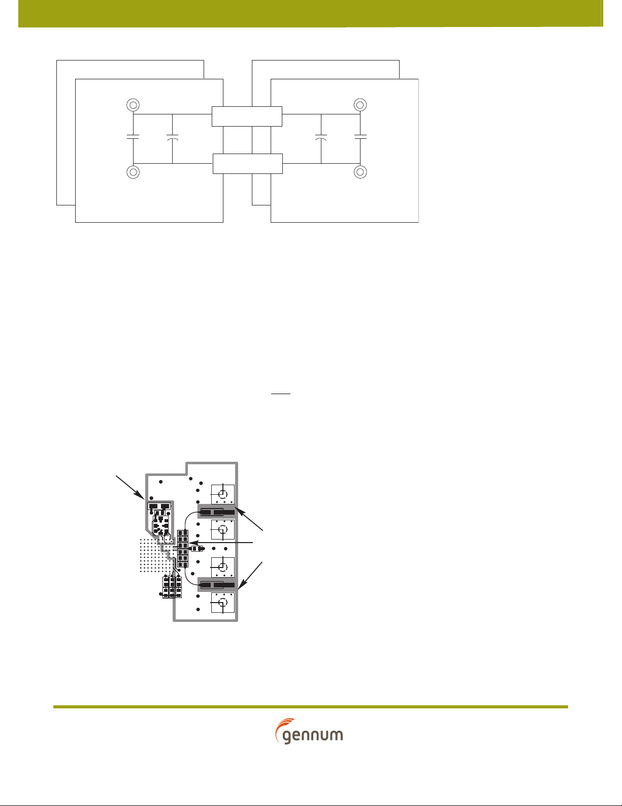
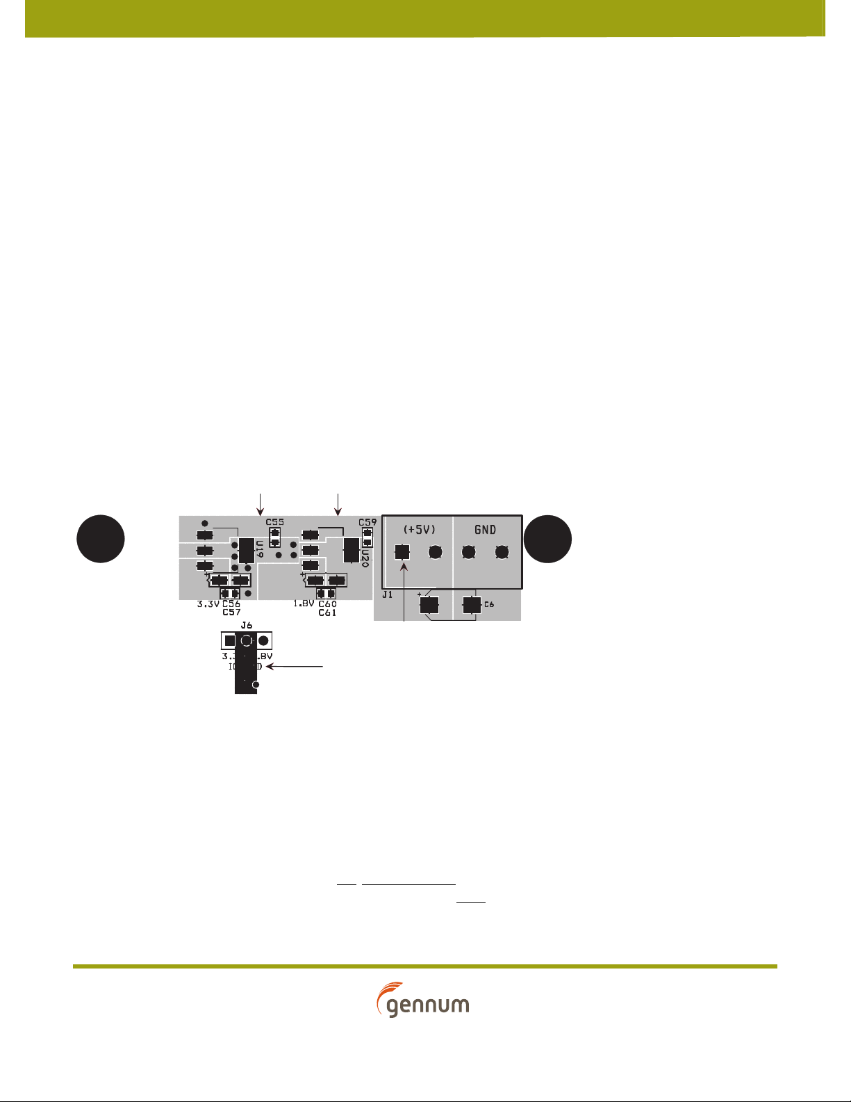
2.1 Power Supply and Ground Isolation
The GS1572 requires two voltages, +3.3V and +1.8V. The +1.8V feeds the digital core,
phase detector and optionally, the digital I/O. The +3.3V feeds the on-chip regulator for
the external VCO and the SDI cable driver. Optionally, the I/O may also use the +3.3V
supply. For optimal performance, it is essential that these supplies be isolated to avoid
external noise coupling. The supplies can be broken down into four components:
1. +1.8V ANALOG - supplying power to the following pins on the GS1572:
PD_VDD/PD_GND (pins A6, B6 and C6, C7, C8)
2. +1.8V DIGITAL - supplying power to the following pins on the GS1572:
CORE_VDD/CORE_GND (pins A5, E1, G10, K8 and B5, C5, D5, E2, E5, E6, E7, F4,
F5, F6, F7, G9, J8)
3. +3.3V ANALOG - supplying power to the following pins on the GS1572:
CP_VDD/CP_GND, CD_VDD/CD_GND (pins A10 and B10, E10 and C9, D9, E9,
F9)
NOTE: Power should be removed from CD_VDD in STANDBY mode for
additional power savings.
4. +3.3V DIGITAL: - supplying power to the following pins on the GS1572:
IO_VDD/IO_GND (pins G1, H10 and G2, H9)
NOTE: Optionally, 3.3V digital can be replaced with 1.8V digital to run with 1.8V
IO.
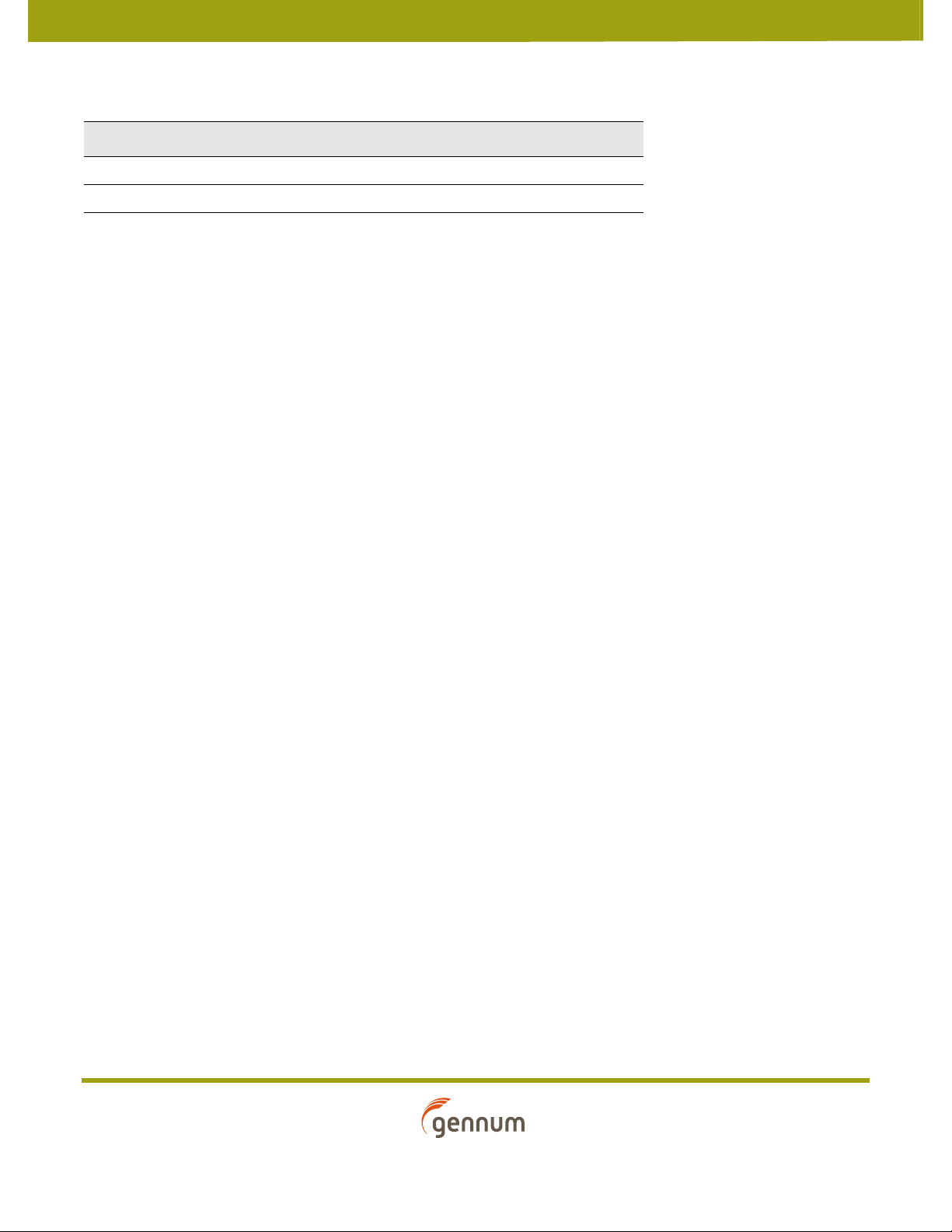
2.1.1 Isolation Methods
Because of the noise sensitive nature of the PLL and analog components of the GS1572,
an isolation technique should be used to filter power to these sections.
Figure 2-1 shows the basic concept behind the technique used. The power plane and
ground plane are isolated from the main plane by a ‘moat.’ Power and ground
connections to the ‘islands’ are made through ferrite beads (0Ωresistors) which are
decoupled on both sides. If possible, running high-speed traces across the moat should
be avoided. Also, any copper (i.e. planes or pours on other layers) which bridge the moat
should be removed.