Service Manual SC-7070, Rev 1.0 26, August, 2003
- 9 -
GSD556 SM_01.doc Gigatelecom Proprietary
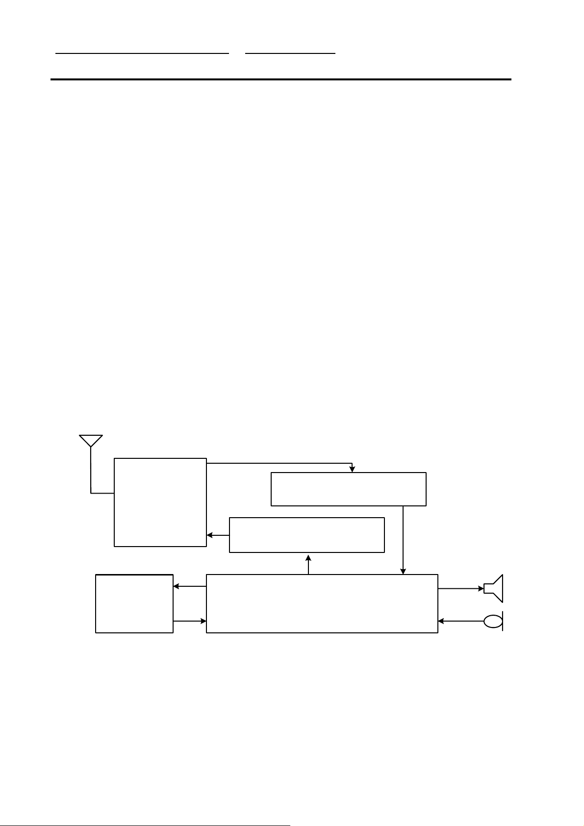
3.2 RF part Description
The RF part consists of power part, synthesizing part, transmission and reception part.
3.2.1 Description of Frequency Synthesizer Circuit
The UHF band frequency synthesizer is composed of an indirect frequency synthesizer, Phase
Locked Loop (PLL IC, U701), VCO(U702) with the center frequency of 966.88MHz for CDMA
mode, Loop Filter and a directional coupler. PLL IC(U701)’s phase detector compares the
reference clock frequency (19.68MHz, TCXO(U705) clock) divided down to 10kHz by the
reference divider with a signal from the VCO(U702) divided by the PLL IC(U701) main divider.
Thus generating local oscillation signals with zero phase difference. These local oscillation signals
are used both for Tx and Rx. The local oscillation signals are separated for Tx and Rx by the
directional coupler. There are Rx and Tx IF synthesizers, respectively. The Tx IF synthesizer is
composed of the RFT3100(U501), Tx Tank circuit, and the loop filter. The Tx phase detector within
the RFT3100(U501) receives the oscillation signals from the tank circuit generating 260.76MHz Tx
IF. The Rx IF synthesizer is composed of the PLL, the S1M8656A01-F0T0(U601), the Rx Tank
circuit, and the loop filter. The signal generated from the tank circuit is sent through the
S1M8656A(U601) to the dual mode PLL’s phase detector. The PLL IC(U701) generates the control
voltage to the loop filter such that 170.76MHz Rx IF is synthesized.
Voltage Control Temperature Compensation Crystal Oscillator (VCTCXO, U705)
The temperature variation of mobile phone can be compensated by VCTCXO(U705). The
reference temperature of a mobile phone is -20~+60 °C. The VCTCXO(U705) receives
frequency tuning signals called TRK_LO_ADJ from MSM as 0.5V~2.5V DC via R and C
filter in order to generate the reference frequency of 19.68MHz and input it into the
frequency synthesizer of UHF band. Frequency stability depending on temperature is
within ±1.5 ppm.
RF Frequency Synthesizer
RF PLL loop is consisted of the RF PLL Synthesizer in the PLL IC(U701), loop filter, VCO
(U702) and VCTCXO(U705). It generates the RF local frequency of 954.38 ~979.38 MHz.
RX IF Frequency Synthesizer
Rx IF PLL Loop is consisted of the Rx IF PLL Synthesizer in the PLL IC(U701), VCO
included in the S1M8656A01-F0T0(U601), loop filter and VCTCXO(U705). The Rx VCO
output included in the S1M8656A01-F0T0(U601) oscillates twice Rx IF frequency of
170.76MHzand then generates the RX IF frequency of 85.38MHz by dividing the VCO
output frequency by two.
TX IF Frequency Synthesizer
The Tx IF PLL Loop is consisted of the Tx IF PLL synthesizer, VCO that is internally
installed in the RFT3100(U501), loop filter and VCTCXO(U702). The Tx VCO output
included the RFT3100(U501) generates Tx IF local frequency of 260.76MHz and then
generates the Tx IF frequency of 130.38MH by dividing the VCO output frequency by two.