Haier HT-3718 User manual

HT-3718
COLOUR TELEVISION
Service Manual
Features
Haier Group
NO: M-EU-CY-HT-3718-9361 Edition:2003.5.20
218 programs stored
Auto-correcting black balance
Blue extension, Green improvement
Multi-picture modes
Fast teletext
Audio/video input, S-Video input, SCART terminal
Model:
HT-3718
(CYPRUS)

1
Contents
1 Contents-----------------------------------------------------------------------1
2Product Code illumination and Series Introduction----------------------2
3 Features----------------------------------------------------------------------------------3
4 Safety Precautions--------------------------------------------------------------------4
5 Warning and Cautions---------------------------------------------------------------5
6 Net dimension--------------------------------------------------------------------------11
7 Parts and Functions------------------------------------------------------------------12
8 Remote Controller Functions-----------------------------------------------------13
9 Program Diagram----------------------------------------------------------------------14
10 Maintenance Service and Trouble shooting----------------------------------15
11 Circuit Diagram-------------------------------------------------------------------------18
12 Circuit Explanation--------------------------------------------------------------------22
13 Adjustment-------------------------------------------------------------------------------27
14 Exploded View--------------------------------------------------------------------------28
15 List of Parts------------------------------------------------------------------------------29
16 Damageable Parts List---------------------------------------------------------------44
17 Information of Resistors and Capacitors--------------------------------------45
CONTENTS

2
2.Product Code illumination and Series Introduction
HT-3718
Product Code illumination and Series Introduction
Color television appearance
haier
CRT size(unit:inch)
Philip

3
1. Features
MODEL
MODEL
NO. ITEM FUNCTION HT-3718
1 Main IC 9361 24 Digital curtain
2 CRT Flat square 25 Slow fading on & off
3 Color system PAL 26 Semitransparent menu
4 Audio system B/G 27 Non-flashing channel changing
5 NO.of channels 218 28 ZOOM
6 OSD language ENGLISH 29 16:9 mode
7
PICTURE
Multi-picture modes 30 Games
8 AV stereo 31 Calendar
9 Super woofer 32 Child-lock
10 Surrounding sound 33 Multi-functional lock
11 Treble/bass boost 34 No-picture listening
12 Left/right balancer 35 Background light
13 NICAM 36 Auto-timer on
14 Multi-audio modes 37 CCD
15 Tone adjuster 38
SOFTWARE
V-CHIP
16 MTS/SAP 39 NO. of built-in speakers 2
17
AUDIO
Auto-volume leveling 40 Audio output power(W) 3
18 AV input back 1 41 Total power input W 70
19 AV output back 1 42 Voltage range V ~180-250
20 DVD terminal 43 Power frequency Hz 50
21 S-video jack 44 Time of sleep timer(MINS) 180
22 Headphone socket 45 Net weight(KG) 11
23
JACK
SCART socket 46 Gross weight(KG) 12
47 Net dimension(MM) 440×355×335
48 Packaged dimension(MM) 475×415×380
49 Quantity for 20' container
50 Quantity for 40' container
51
PARAMETER
Quantiry for 40' high container
Functures

4
4.Safety Precautions
SAFETY PRECAUTIONS
IMPORTANT SAFETY NOTICE
Many electrical identify these parts and mechanical parts in this chassis have special
safety-related characteristics! In the Schematic Diagram and Replacement Parts List.
It is essential that these special safety parts should be replaced with the same components as
recommended in this manual to prevent X-RADIATION, Shock, Fire, or other Hazards.
Do not modify the original design without permission of the manufacturer.
General Guidance
An Isolation Transformer should always be used during the servicing of a receiver whose chassis
is not isolated from the AC power line. Use a transformer of adequate power rating as this protects
the technician from accidents that might result in personal injury caused by electrical shocks.
It will also protect the receiver and it’s components from being damaged by accidental shorts of the
circuitry that might be inadvertently introduced during the service operation.
If any fuse (or Fusible Resistor) in this TV receiver is blown, replace it with a specified one.
When replacing a high wattage resistor (Oxide Metal Film Resistor, over 1W), keep the resistor
10mm away from PCB.
Keep wires away from high voltage or high temperature parts.
Due to the high vacuum and large surface area of the picture tube, extreme care should be taken
in handling the Picture Tube. Do not lift the Picture Tube by its Neck.
X-RAY Radiation
Warning:
The source of X-RAY RADIATION in this TV receiver is the High Voltage Section and the Picture
Tube.
For continued X-RAY RADIATION protection, the replacement tube must be of the same type as
specified in the Replacement Parts List.
Before returning the receiver to the customer,
Always perform an AC leakage current check on the exposed metallic parts of the cabinet, such as
antennas, terminals, etc., to make sure that the set is safe to operate without any danger of
electrical shock.
Safety Precautions

5
5. Warning and Cautions
Warning and Cautions
CAUTION: Before servicing receivers covered by this service manual and its supplements and
addenda, read and follow the SAFETY PRECAUTIONS.
NOTE: If unforeseen circumstances create conflict between the following servicing precautions
1. When
y
ou clean the TV set, please pull
out the power plu
g
from AC outlet. Don't
clean the cabinet and the screen with
benzene, petrol and other chemicals.
4. To prevent the TV set from firing and
electric shock, don't
make the TV set rain
or moisture.
2.
In order to prolon
g
the usin
g
life of the
TV set, please place it on a ventilated
place.
5. Don't open the back cover, otherwise it is
possible to damage the components in the
TV set and harm you.
3.
Don't place the
TV set in the
sunshine or near
heat source.
6. When the TV set isn't going to be used
for long time or it is in thunder and
lightening, please pull out the plug from AC
outlet and the antenna plug from the cover
of the TV set.
Explanation on the display tube
Generall
y
, it is not needed to clean the tube surface. However, if necessar
y
,its surface can be
cleaned with a dr
y
cotton cloth after cuttin
g
off the power.Don't use an
y
cleanser. If usin
g
hard
cloth, the tube surface will be damaged.
Warning and Cautions

6
and any of the safety precautions, always follow the safety precautions. Remember: Safety First.
General Servicing Precautions
5.1 Always unplug the receiver AC power cord from the AC power source before:
a. Removing or reinstalling any component, circuit board module or any other assembly of
the receiver.
b. Disconnecting or reconnecting any receiver electrical plug or other electrical connection.
c. Connecting a test substitute in parallel with an electrolytic capacitor in the receiver.
CAUTION: A wrong substitution part or incorrect installation polarity of electrolytic
capacitors may result in an explosion hazard.
d. Discharging the picture tube anode.
5.2Test high voltage only by measuring it with an appropriate high voltage meter or other
voltage-measuring device (DVM, FETVOM, etc.) equipped with a suitable high voltage probe.
Do not test high voltage by “drawing an arc”.
5.3 Discharge the picture tube anode only by (a) first connecting one end of an insulated clip lead
to the degaussing or kine aquadag grounding system shield at the point where the picture tube
socket ground lead is connected, and then (b) touch the other end of the insulated clip lead to
the picture tube anode button, using an insulating handle to avoid personal contact with high
voltage.
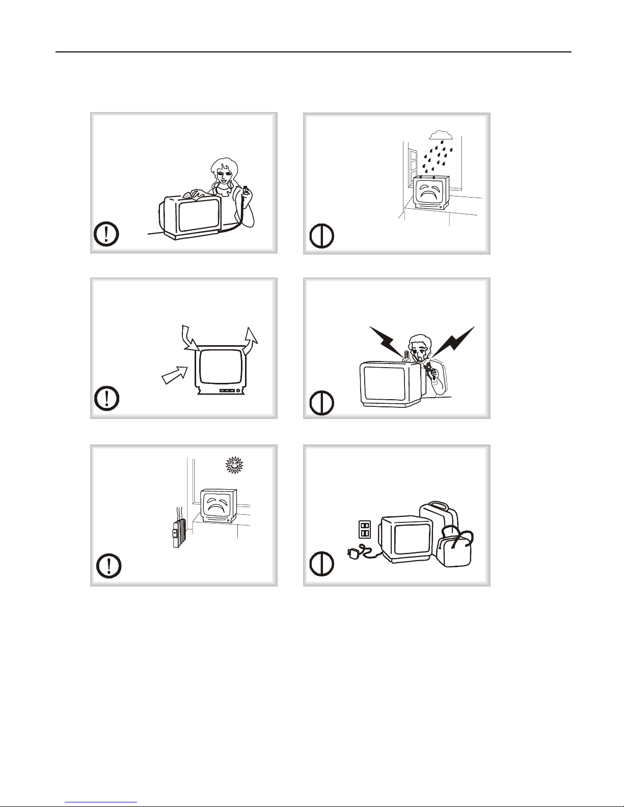
5.4 Do not spray chemicals on or near this receiver or any of its assemblies.
5.5 Unless specified otherwise in this service manual, clean electrical contacts only by applying
the following mixture to the contacts with a pipe cleaner, cotton-tipped stick or comparable
nonabrasive applicator; 10% (by volume) Acetone and 90% (by volume) isopropyl alcohol
(90%-99% strength)
CAUTION: This is a flammable mixture.
Unless specified otherwise in this service manual, lubrication of contacts is not required.
5.6 Do not defeat any plug / socket B+ voltage interlocks with which receivers covered by this
service manual might be equipped.
5.7 Do not apply AC power to this instrument and/or any of its electrical assemblies unless all
solid-state device heat sinks are correctly installed.
5.8 Always connect the test receiver ground lead to the receiver chassis ground before
connecting the test receiver positive lead.
Always remove the test receiver ground lead last.
5.9 Use with this receiver only the test fixtures specified in this service manual.
CAUTION: Do not connect the test fixture ground strap to any heat sink in this receiver.
Electrostatic ally Sensitive (ES) Devices
Some semiconductor (solid state) devices can be damaged easily by static electricity. Such
components are usually called Electrostatic ally Sensitive (ES) Devices. Examples of typical ES
Warning and Cautions

7
devices are integrated circuits and some field effect transistors and semiconductor “chip”
components. The following techniques should be used to help reduce the incidence of component
damage caused by static electricity.
a. Immediately before handling any semiconductor component or semiconductor- equipped
assembly, drain off any electrostatic charge on your body by touching a known earth ground.
Alternatively, obtain and wear a commercially available discharging wrist strap device, which
should be removed to prevent potential shock prior to applying power to the unit under test.
b. After removing an electrical assembly equipped with ES devices, place the assembly on a
conductive surface such as aluminum foil, to prevent electrostatic charge buildup or exposure
of the assembly.
c. Use only a grounded-tip soldering iron to solder or unsolder ES devices.
d. Use only an anti-static type folder removal device. Some solder removal devices not
classified as “anti-static” can generate electrical charges sufficient to damage ES devices.
e. Do not use freon-propelled chemicals. These can generate electrical charges sufficient to
damage ES devices.
f. Do not remove a replacement ES device from its protective package until immediately before
you are ready to install it. (Most replacement ES devices are packaged with leads electrically
shorted together by conductive foam, aluminum foil or comparable conductive material).
g. Immediately before removing the protective material from the leads of a replacement ES
device, touch the protective material to the chassis or circuit assembly into which the device will
be installed.
CAUTION: Be sure no power is applied to the chassis or circuit, and observe all other safety
precautions.
h. Minimize bodily motions when handling unpackaged replacement ES devices. (Otherwise
even some normally harmless motions such as mutual brushing of your clothes’ fabric or lifting
of your foot from a carpeted floor might generate static electricity sufficient to damage an ES
device.)
General Soldering Guidelines
a. Use a grounded-tip, low-wattage soldering iron and appropriate tip size and shape that will
maintain tip temperature within the range of 500 oF to 600 oF.
b. Use an appropriate gauge of RMA resin-core solder composed of 60 parts tin/40 parts lead.
c. Keep the soldering iron tip clean and well tinned.
d. Thoroughly clean the surfaces to be soldered. Use a mall wire bristle (0.5 inch, or 1.25cm)
brush with a metal handle. Do not use freon-propelled spay-on cleaners.
e. Use the following unsoldering technique
a). Allow the soldering iron tip to reach normal temperature. (500 o F to 600o F)
b). Heating the component lead until the solder melts.
Warning and Cautions

8
a. draw the melted solder with an anti-static, suction-type solder removal device with solder
braid.
CAUTION: Work quickly to avoid overheating the circuit board printed foil.
f. Use the following unsoldering technique
A). Allow the soldering iron tip to reach normal temperature. (500 o F to 600o F)
B). First, hold the soldering iron tip and solder the strand against the component lead until the
solder melts.
C). Quickly move the soldering iron tip to the junction of the component lead and the printed
circuit foil, and hold it there only until the solder flows onto and around both the component lead
and the foil.
CAUTION: Work quickly to avoid overheating the circuit board printed foil.
D). Closely inspect the solder area and remove any excess or splashed solder with a small
wire-bristle brush.
Remove /Replacement
Some chassis circuit boards have slotted holes (oblong) through which the IC leads are inserted
and then bent flat against the circuit foil. When holes are of slotted type, the following technique
should be used to remove and replace the IC. When working with boards using the familiar round
hole, use the standard technique as outlined.
Removal
Desolder and straighten each IC lead in one operation by gently prying up on the lead with the
soldering iron tip as the solder melts.
Draw away the melted solder with an anti-static suction-type solder removal device (or with solder
braid) before removing the IC.
Replacement
Carefully insert the replacement IC in the circuit board.
Carefully bend each IC lead against the circuit foil pad and solder it.
Clean the soldered areas with a small wire-bristle brush. (It is not necessary to reapply acrylic
coating to the areas).
“Small-Signal” Discrete Transistor
Removal/Replacement
Remove the defective transistor by clipping its leads as close as possible to the component body.
Bend into a “U” shape the end of each of three leads remaining on the circuit board.
Bend into a “U” shape the replacement transistor leads.
Connect the replacement transistor leads to the corresponding leads extending from the circuit
board and crimp the “U” with long nose pliers to insure metal to metal contact then solder each
connection.
Power Output, Transistor Device
Warning and Cautions

9
Removal/Replacement
Heat and remove all solder from around the transistor leads.
Remove the heat sink mounting screw (if so equipped).
Carefully remove the transistor from the heat sink of the circuit board.
Insert new transistor in the circuit board.
Solder each transistor lead, and clip off excess lead.
Replace heat sink.
Diode Removal/Replacement
Remove defective diode by clipping its leads as close as possible to diode body.
Bend the two remaining leads perpendicularly to the circuit board.
Observing diode polarity, wrap each lead of the new diode round the corresponding lead on the
circuit board.
Securely crimp each connection and solder it.
Inspect (on the circuit board copper side) the solder joints of the two “original” leads. If they are not
shiny, reheat them and if necessary, apply additional solder.
Fuse and Conventional Resistor
Removal/Replacement
a. Clip each fuse or resistor lead at top of the circuit board hollow stake.
b. Securely crimp the leads of replacement component around notch at stake top.
c.Solder the connections
CAUTION: Maintain original spacing between the replaced component and adjacent
components and the circuit board to prevent excessive component temperatures.
Circuit Board Foil Repair
Excessive heat applied to the copper foil of any printed circuit board will weaken the adhesive that
bonds foil to the circuit board causing the foil to separate from or “lift-off” the board. The following
guidelines and procedures should be followed whenever this condition is encountered.
At IC Connections
To repair a defective copper pattern at IC connections use the following procedure to install a
jumper wire on the copper pattern side of the circuit board. (Use this technique only on IC
connections).
a. Carefully remove the damaged copper pattern with a sharp knife. (Remove only as much
copper as absolutely necessary).
b. Carefully scratch away the solder resist and acrylic coating (if used) from the end of the
remaining copper pattern.
c. Bend a small “U” in one end of a small gauge jumper wire and carefully crimp it around the IC
Warning and Cautions

10
pin. Solder the IC connection.
d. Route the jumper wire along the path of the out-away copper pattern and let it overlap the
previously scraped end of the good copper pattern. Solder the overlapped area and clip off any
excess jumper wire.
At other connections
Use the following technique to repair the defective copper pattern at connections other than IC
Pins. This technique involves the installation of a jumper wire on the component side of the circuit
board.
a. Remove the defective copper pattern with a sharp knife.
Remove at least 1/4 inch of copper, to insure that a hazardous condition will not exist if the
jumper wire opens.
b. Trace along the copper pattern from both sides of the pattern break and locate the nearest
component that is directly connected to the affected copper pattern.
c. Connect insulated 20-gauge jumper wire from the lead of the nearest component on one side of
the pattern break to the lead of the nearest component on the other side.
Carefully crimp and solder the connections.
CAUTION: Be sure the insulated jumper wire is dressed so that it does not touch components or
sharp edges.
Warning and Cautions

11
6. Net dimension
HT-3718
Net dimension
Front view
Side view
Top-view

12
7. Parts and Functions
Remote sensor:let The remote controller aim here the set can receive remote
control signal.
Power switch:Press the button to turn on the TVset . press the button again to turn
off the TV set.
Power indicator: the indicator lights when power on .
Menu button
program up/down button
Volume up/down button
TV/AV
2.Rear Panel
1.Front Panel
S-VIDEO input
SCART socket
Antenna input
FUNCTION BUTTONS AND EXTERNAL SOCKETS
S-VIDEO SCART
Audio (R) input
Audio (L) input
Video input
11
12
13
11
12
13
Parts and Functions

13
8. Remote Controller Functions
Remote Controller
MARK FUNCTION DESCRIPTION
Mute
Standby
ONEDIGITSELECTION
TV/VIDEO SELECTION
MENUDISPLAY
VOLUMECONTROL
CHANNELNUM BER UP/DOW N
0-9
-/--
TV/AV
MENU
SW AP
-VOL+
-C H + PICTURE MENU
SOUND MENU
SOUND TIM E MENU
TIM E FUNCTION MENU
FUNCTION
123
PICTURE
P.
P
?
NOTE
Thefu n ction ofselecting m enu button on the rem ote controlleris
th e sam e as th a t ofprogram up/dow n button on th e TV set.
Thefuction ofidentifying m enu button o n th e rem o te co n tro ller
is th e sam e as th at ofvolum e up/dow n button on the TV set.
Program scan
TELETEXT SUBTITLE
A2/NICAM/MONO SOUND SELECTION
PICTURE MODESELECTION
NO USED
TUNE M ENU SELECTION
TV/TELETEXT ENTERING/EXITING
TO REVEALCONCEALED TELETEXT
TELETEXT ZOOM
TELETEXT PAGE HOLD
TELETEXT/TV MIXMODE
TV/TELETEXT ALTERATION
EAST/W EST
EXITMENU DISPLAY
REM OTE CONTROLLER BOARD
Remote Controller Functions

14
9. Program Diagram
Insert the power plug into the power line socket and insert the antenna plug into the antenna
socket on the rear panel. Press down the power switch of the TV set. The red indicator light goes
on. If no picture appears, press the button on the remote controller. Follow the steps below.
AProgram preset
1. Auto searching and storing program
Press MENU button on the remote controller then use the “CH+/CH-“ key to call up the “tune
program” menu on the screen. Then Press the menu” VOL+/VOL- “ item to adjust. it.Use the
“CH+/CH- ” key to select the bar “auto search program” then press the “VOL+/VOL-” to make
sure. If you want to stop ,press the key “ MENU ”.
2. Manual search and fine tune
Press MENU button then use the “CH+/CH-“ key to call up the “tune program” menu on the
screen. Then Press the menu” VOL+/VOL- “ item to adjust. it.Use the “CH+/CH-” key to select
the bar “Manual search program” then press the “VOL+/VOL-” to make sure.
3.Deleting channel number
Press Program up/down buttons to select a channel to skip. Press MENU to call Menu. then
use the “CH+/CH- “ key to call up the “tune program” menu on the screen. Then Press the
menu” VOL+/VOL- “ item to adjust. it.Use the “CH+/CH-” key to select the bar “Cannal
number” then press the “VOL+/VOL-” to make sure. Enter the number that you do not want to
see .Then Then select “SKIP” and select SKIP to ON. Now the program number is deleted.
Repeat the above steps and select SKIP to OFF, the deleted program number can be resumed.
BVolume tuning
Press VOLUME buttons VOL+ to increase and VOL- to decrease the volume.
C Personal preference settings
Picture modes
Press SELC PICTURE repeatedly to change among MEMORY 1, MEMORY2,MEMORY3,to chang
the Picture Mode.
Program Diagram

15
10.Maintenance Service and Trouble shooting
a.Factory adjustment information
Operation method: after the appliance is switched on, press MUTE CALL -/-- CALL MUTE
Button in turn and enter service mode.
Press PRO- and PRO+ buttons to select items for adjustment.
Press VOL- and VOL+ buttons to adjust selected items.
Press the POWER button to switch off the appliance and go back to the normal state.
Maintenance menu (Table 8)
Item Specifications Default Value
Variable
Mark
5PAR Horizontal parabola *
5BOW Horizontal Bow *
5HSH Horizontal shife 40 *
5EWW EW width *
5EWP EW parabola *
5UCR EW upper corner parabola
5LCR EW lower corner parabola
5EWT EW trapezium
5VSL Vertical slope 42
5VAM Vertical amplitude 55
5SCL S-Correction 21
5VSH Vertical Shift 28
5VOF OSD Vertical Offset 40
HOF OSD Horizontall Offset 40
VX Vertical Zoom
6PAR Horizontal parabola
6BOW Horizontal Bow
6HSH Horizontal shife
6EWW EW width
6EWP EW parabola
6UCR EW upper corner parabola
6LCR EW lower corner parabola
6EWT EW trapezium
6VSL Vertical slope
6VAM Vertical amplitude
6SCL S-Correction
6VSH Vertical Shift
6VOF OSD Vertical Offset
HOF OSD Horizontall Offset
VX Vertical Zoom
RED Black level offset R 32 *
GRN Black level offset G 32 *
Maintenance Service and Trouble shooting

16
Item Specifications Default Value Variable
Mark
WPR White point R 31 *
WPG White point G 26 *
WPB White point B 31 *
YDFP Y-Delay for PAL 7 *
YDFN Y-Delay for NTSC *
YDAV Y-Delay for AV *
TOP AGC Take-Over point 32 *
VOL Volume 44
9874 Output Gain of TDA9874A 26
AVLT TDA9874A AVL decay time 1
9860 Sub volume of TDA9860/59 69
IFFS Vision IF 2
HDOL Cathode drive level 5
AGC IF AGC speed 1
VF2B VG2 Brightness 50
0CON Listen:Contrast 0
0BRI Listen:Brightness 0
0COL Listen:Color 50
0SHP Listen:Sharpness 50
1CON Soft: Contrast 45
1BRI Soft: Brightness 45
1COL Soft: Color 50
1SHP Soft: Sharpness 50
2CON Standard: Contrast 70
2BRI Standard: Brightness 50
2COL Standard: Color 60
2SHP Standard: Sharpness 50
3CON Dynamic: Contrast 80
3BRI Dynamic: Brightness 50
3COL Dynamic: Color 70
3SHP Dynamic: Sharpness 50
OP1 Option 1 177
OP2 Option2 127
OP3 Option3 255
OP4 Option4 75
OP5 Option5 183
OP6 Option6 89
OP7 Option7 1
You can change the DATA with “*” mark when necessary.
Maintenance Service and Trouble shooting

17
Check to see if
Fuse3 is normal
No light and sound
Abnormal
Check VD503-VD,
506,C511, N501, etc.
Check to see if the
collector voltage of
VD512is 24V
Check
N507,N508
Check to see
if , 8v,
5v is normal
Check the control
voltage of VD512
or CPU power
The failure of
horizontal unit or
N201
Normal
Normal
Normal Abnormal
Check to see 110V 180V
etc. voltage is normal
Test to see all terminal
Resistance of load
Is normal
Check switch
p
ower unit
Check to see if
rectifying tube
is normal
Change
rectifying tube
Check the
Loader
A
bnormal
Normal
Abnormal
Normal Abnormal
Normal Abnormal
Maintenance Service and Trouble shooting

11. Circuit Diagram
Circuit Diagram
12345678910 11 12
A
B
C
D
12
1110987654321
D
C
B
A
R009
3. 3K
MAI N BOARD
!
AV-IN
XP502
*
R2
!
L2
V2
!
!
SW006
SW005
!
R008
1. 8K
R007
1. 2K
!
R006
1k
R005
620
!
SW007
SW004
!
SW003
SW002
!
R002
470
TV/AV
!
MENU
CH+
!
CH-
VOL+
!
VOL-
!
R54 6
10K
V509
2SB892
R50 3
1. 5K
V508
2SC536
A0
A1
A2
GNDSDA
SCL
TEST
VCC
N202
AT24C04/08
VD001
SLP-177B
C60 0
50V 470uF
R410 82
+5V
R411 82
C60 2
16V 100uF
12345678910
N301 LA4285/87 (R)
12345678910
N302 LA4285/87 (L)
220V
C311
10/ 16V
220V
R322
10k C302
0. 01
RLP1
LK1aF-12V
R321
4. 7k C321
10/ 16V
L01
谐波抑制器
C312
0. 01u
R304
4. 7k
R312
10k
STANDBY
R603
10K
R604
10K
+5V
XS302
VD605
1N4148
V601
2SC536
V602
2SC536
C310
25V/470u
In Out
Gnd
N602
7805
C307
0. 01u
C306
25V/ 1000u
EM0 1Z
VD601
VD604
D?
DIODE
C321
25V/470u
220V
R310
680
TP1
DB-1. 3-08
R320
680
C324
100/ 16V
VD321
1N4148 VD311
1N4148
L.OUT
C318
16V/100u
R.OUT
NC
NC
NC
GND
6
5
4
3
2
C314
16V/100u
1
C323
100/ 16V
SA:
C329
2. 2/ 50V
FM I N
C315
50V/2.2u
6
C316
0. 01u
SDA
C325
0. 01
5
3SCL
+5V (+8V)
GND
4
2
1 NC
0
SB:IFIN
R528
0. 5W8. 2M
V333
2SC1815
R332
10k
V331
2SA1015
VD331
1N4148
C40 4
22nF
C319
16V/100u
C40 3
22nF
R330
10k
R93 1
3. 3K
V332
2SC1815
R90 5
100
R314
10k
8W/ 8OHM
C95 9
4. 7uF
+8V
R44 1
4K7
V403
C18 1 5 R4 4 0
4K7
+8V
C11 5
0. 01uF
+8V
C92 4
0. 22uF
L80 2
2uH
6. 8mH
L90 5
R91 6
100 2W
+12V
C92 6
330n/500V
20V
C88 0
220nF
XS306
12
R303
100 R302
100
RL
C303
0. 015 C313
0. 015
R331 4. 7k
R329 4. 7k
R328
10k
R324
4. 7k
C331
10/ 16V
C328
10/ 16V
C326 0. 01
C330
0. 01
R412 82
R21 1
3. 3K
R21 6
3. 3K
R21 5
3. 3K
R20 9
100
C20 6
0. 01uF
R20 7
100
R20 8
100
C20 8
56PF C20 7
56PF
R21 0
4K7
+5A
R21 7
1K
R21 8
47
C20 9
0. 022uF
Lr ef
ADDR2
Vssa2
Vdec
R00 0
180
TEST1
+3. 3V
SI F2
Vref1
SI F1
CRESET
VSSa3
Vdda3
R21 9
1. 2K
SCL
R22 2
1. 2K
SDA
R22 0
3. 3K
SDO
R22 1
27K
WS
R22 5
27K
SCK
SYSCLK
Vddd3
Vssd3
P1
TEST2
XTAL1
XTALO
ADDR1
+5V
PCLK
TP1
NICAM DATE OUT
TP2
Vssd2
Vddd1
Vssd1
C22 7
1nF
Vssa1
R23 5
15k
Vdda1
C22 0
1uF
Vssa4
OUT M
P2
C21 5
22nF
Vref 2
C21 2
100uF
EXTIL
EXT I R
L205
10uH
+8V
MONOIN
R23 7
100
OUT R
R23 8
100
OUT L
C22 8
1nF
C21 9
4. 7nF
61
SA
SB
C23 1
22nF
R24 1
680
R23 6
100K
R24 0
10K
+5V
C108
16V/100u
AGC
TU
U/V
H/L
BM
IF
LAN
U201
TDQ
C109
0. 01u
L101
10uH
LN05
1uH
C11 0
0. 01uF
LN03
1uH
+5V
16
15
C10 1
4. 7uF
14
R10 1
6. 8K
13
12
11
10
C10 2
0. 01uF
9
R10 2
4K7
8
7
C10 3
100nF
6
R20 2
10K
5
C20 1
100nF
4
R20 1
10K
17
18
42
41
40
39
38
37
36
35
34
V103
2SC1815
33
R205
12k
32
31
30
29
28
27
26
+5V
C20 5
10uF/50V
25
R20 6
10K/3W
24
DZ203
UPC574
23
2221
20
19
3
2
1
NN02
TDA9874APS
+110V
C10 5
10uF
C10 6
10uF
R19 9
10K
+
CN35100uF
R19 8
10K
R23 0
4. 7K
R23 1
4. 7K
RN18
10
CN32
0. 022uF
RN12
6. 8
CN05
0. 022uF
RN07
10
C19 9
0. 01uF
R10 7
2. 2K
R10 8
4. 7K
CN03
1nF
RN05
150K
R11 0
180
RN06
2. 7K
R11 1
22
VN01
BF3 7 0
V101
2SC2216
CN16
100pF
R11 2
10
L102
1uH
C11 2
0. 01uF
R11 9
4K7R11 7
2. 2K
R11 8
3. 3K
RN17
2K
R11 6
56K
CN15
8. 2pF
R11 5
82K
LN02
1. 8uH
VD101
BAT81
V102
2SC1815
CN12
0. 022uF
+8V
RN16
22K
RN15
22K
CN10
0. 022
+
CN11
10uF
+
CN09 2.2uF
ZN01
k9261
ZN02 coi l
38M
Z20 1
K7266
+
CN08
2. 2uF
CN07
22nF
CN06
0. 1uF
RN10
390
RN08
10K
RN09
2. 7K
VIF1 1
VIF2 2
TOP3
CCS 4
MUTE 5
Tpl l 6
Vo-CVBS 7
n. c. 8
Vo-AF9
Ca f 10
Vi-IC
11
TAGC
12
Vo(vi d)
13
Vi ( vi d)
14
AFC
15
VCO1
16
VCO2
17
GND
18
Ca gc
19
Vp
20
TDA9801
NN01
CN23
0. 47uF
+
CN20 2.2uF
CN19 0. 01uF
+
CN17
47uF
+8V
CN31
0. 47uF
R22 7
5. 6K
CN22
0. 47uF
R22 6
5. 6K
C21 6
10uF
CN18
0. 01uF
C21 0
10uF
R23 2
3. 3K
RN25
3. 3
R22 8
3. 3K
RN20
100
+
CN21 2.2uF
RN19
8. 2K
CN25
0. 47uF
CN26
0. 1uF
RN22
100
R28 2
47
ZN03
24.576MHz
R21 3
3. 3K
CN29
0. 47uF
R21 2
3. 3K
CN30
0. 47uF
RN23
100
L271
10uH
+
CN28
1uF
C27 1
22nF
C27 2
10uF
12MHz
Z20 2
C27 0
33pF
C26 9
33pF
L270
10uH
C27 5
47uF
L260
10uH
C26 7
22nF
C26 8
100uF
R27 6
100
R27 5
100
R27 2
100
R27 0
2. 2K
VD203
1N4148
VD202
1N4148
VD201
1N4148
C26 6
1000pF
C92 5
0. 22uF
R93 0
1. 5K
VD910
1N4148
C26 0
0. 1uF
R24 8
5. 6K
C24 8
1000pF
C24 5
1. 0uF
C24 2
1. 0uF
C24 6
22nF
C24 7
100uF
L201
10uH
R24 7
390
C24 1
100nF
R26 7
27K
C22 9
1nF
R26 6
100K
C24 0
4. 7uF
R26 2
27K
R24 5
1. 8K
R25 0
1. 8K
+8V +8V
V250
2SC1815
V256
2SC1815
V252
2SC1815
V255
2SC1815
XT6. 0
Z25 1
XT6. 5
Z25 0
XT4. 5
Z25 5
XT5. 5
Z25 2
R26 5
47
+8V
C25 0
47uF
R25 1
180
R25 5
100
R317
22 C317
0. 1u
L252
6. 8uH
L250
8. 2uH
R25 2
150
8W/ 8OHM
XS302
R25 6
220
R26 8
1. 5K
R25 7
470
VD701
ERC24- 06
GND
R25 9
2. 2K
R25 8
4K7
TDA6107Q
N7 0 1
R26 0
39
R26 1
100
C70 9
391
C70 8
391
R70 7
100
R70 8
100
DZ70 2
MTZJ9. 1B
DZ70 3
MTZJ9. 1B
987654
3
R25 3
10K
21
3. 0
114
116
111
178. 5
6. 0
3. 0
3. 0
R71 1
100
R71 2
100
VD704
ERB4304
VD703
ERB4304
C70 2
222
+8V
C70 4
4. 7u
R24 9
1. 2K
PROBE1
PROBE2
PROBE3
VDDV3V2V1
2
XS001
XS5
1
3
R70 3
1. 8K
R70 1
1. 8K
R70 2
1. 8K
R70 4
10M
CRT
+3. 3V
C70 3
103
HV
SC
FO
+5V
V
V Dr v _
V Dr v +
R80 6
2. 2/ 1W
R802 2. 2K
1
R81 0
270/ 2W
R80 7
33/ 0. 5W
C80 9
47nF/ 100V
R81 2
5. 6K
+C80 6
22uF/63V
+
C80 5
220uF/ 25V
1
2
3
4
5
X902
CON5
R71 0
100
1
R81 1
1. 5
H
R72 7 3 3 K
L90 1
H-LINE
C70 6
10u
EHT
VD905
BYV95B
VD906
BYD33G
R91 1
2.2/ 0. 5W
VD907
BYD33J
C91 2
470pF/ 500V
Focu s
G2
+
C91 7
220uF/ 25V
VD702
ERB4304
+C91 6
100uF/ 63V
DZ70 4
MTZJ9. 1B
+
C91 5
4.7uF/ 250V
DZ70 1
MTZJ9. 1B
R92 0
220K
C70 7
391
R70 5
2. 4
R80 3
2. 2K
R72 6
68
R70 9
100
+C92 1
1uF/160V
GT702 1P
7
R91 2
6. 8
GT701 1P
+
C90 9
10uF/ 160V
Gnd
+110V
1
2
3
4
X903
CON4
R92 7
2. 2
R92 2
1K
R92 5
5. 1K*
C92 0
100nF
VD911
1N4148
8
7
6
DZ90 1
BZX79C15V
5
R91 7
680
4
R91 8 1K
3
VD908
1N4148
2
1
T90 1
H-DRI VER
2
R907 270
CN702
C90 2
4700pF/ 500V
CN701
R908 2. 2K
CN703
1
+
C90 1
47uF/50V
+24V
R90 2
100
2
R91 0
82
3
C90 6
5n6/ 2KV
C90 8
8n2/ 2KV
C91 8
390 n/ 250 V
5
V957
D2012
R97 6
6. 8K
R97 5
100K
4
R97 9
1K
1
R92 6
4. 7K
R90 1
3. 9K
C90 5
220pF/ 500V
3
DZ90 0
BZX79C8V2
C95 3
0. 22uF
2
C95 8
0. 47uF
1
+8V
V951
C18 1 5
R96 7
1K
R96 9
820
R968 1. 5K
R97 0
270
R95 0
5. 6K
R96 6
10
R97 1
1. 5K
R97 2
10K
+C95 0
10uF/16V R97 7
220K
C91 0
1000pF/ 500V
V901
BF422L
V952
C18 1 5
Gnd
R97 8
39K
R95 9
2. 2K
I+
1
I-
2
Vp
3
VOB
4
Gnd
5
VFB
6
VOA
7
Vguar d
8
VIFB
9
N801
TDA8357
C80 1
2. 2nF
C80 2
2. 2nF
R81 3
2. 7K
CN000
1
2
3
+
C51 5
100 uF/ 16 V
V902
BU2508DX
In Out
Gnd
N506
7805
R53 7
2. 2K
2
1
3
4
5
6
7
8
9
10
11
12
13
T90 2
FBT2
L01
谐波抑制器
14V
43V
R80 1
33K
C80 7
220nF
C80 8
0. 01uF
L80 1
2uH
PCT817C
VD507
ABL
R57 9
10K
VD572
1N4148 V571
KSC815
R57 6
15K
R58 1
22K
R57 3
2. 49K
Audi o 2
R57 1
127K
KA431
N571
R91 5
1K 0. 5W
R57 7
39K
C57 1
104
R59 1
1. 5K
V950
2PA1015
R57 2
1K
R98 0
6. 8K
C91 3
0. 033uF/630V
C95 7
0. 1uF
VD912
BY228
R52 1
2. 2K
+
C52 2
100uF/ 35V
+24V
VDrv+
C52 1
470pF/ 500V
VD511
BYD33D
+
C95 2
100 uF/ 16 V
+
C95 6
470uF/ 6. 3V
+C95 1
10uF/50V
R50 0 A
470K
R50 0 B
470K
C95 5
0. 1uF
R51 7
600
C51 3
47u
V956
2PA1015
RP9 5 1
47K
RP9 5 0
10K
VD520A
B12 0 6 VD520
ERB4304
VD596
IN4148
R95 5
2. 7K
R57 8
470
R95 1
56K
C59 8
392
R95 2
18K
SYNC
R98 1
6. 8K
2
1
53
VD950
1N4148
4
VCC
VFB
N501
L90 2
600uH
R95 6
5. 6/ 1W
C53 1
222
L50 4
F/ B
R327
22
H.WIDTH
C327
0. 1u
PI NC
VD312
1N4148
Video Out
VD310
1N4148
R93 2
120K
VD320
1N4148
Video/SVHS- Y
SVHS- C
Cr
R311
1k
YCb
SYS
VOL1VOL2
Ba nd 2 Ban d 1
VOL2
VDrv-VDrv+
R99 9
39K
AGC
R96 4
470K
C23 9
1. 0uF
C23 8
330pF
C23 6
10uF
473
C51 4
R51 1 A
33K
R51 5 A
33K
C23 7
1. 2nF
R24 2
3. 9K
C23 5
6800pF C23 2
100nF R23 9
39K
C23 0
3. 3uF
C22 6
2. 2uF
C22 5
22nF
1
2
3
7
9
10
11
12
13
14
15
16
T50 1
C22 2
2. 2nF C22 1
220nF C21 8
220nF
1
2
3
CP1 01 I R
C13 2
10nF
Gnd
12. 5V
+5A
AGC
Tuning
110V
Ba nd 1
standby
Ba nd 2
SYS
Tuning
AV1
DZ50 6
BZX79C2V7
R54 1
1K
R54 0
1K
VOL1
V541
C18 1 5
V540
C18 1 5
VD299
1N4148
VD298
1N4148
R29 9
3. 3K
+5V-1
VD297
1N4148
Gnd
V299
2SC1815
R53 9
430
R29 6
1K
DZ59 5
BZX79C5V1
R29 7
10K
+16V
+
C53 5
470uF/ 25V
SW
SW
+
C53 8
100uF/ 16V
+3. 3V
+5V
+8V
R53 8
56/ 2W
R42 5
470
+
C53 7
470uF/ 35V
R42 6
100K
+
C53 4
100 uF/ 16 V
R420 100K
R41 8
68
+
C54 7
100uF/ 16V
R42 1
470
V401
C18 1 5
In Out
Gnd
N507
7805
V402
C18 1 5
+
C53 7
470uF/ 25V
X105
S- VHS
R53 6
1/ 1W
+
C40 6
1uF/16V
+
C40 5
10uF/16V
+24V
+
C40 7
1uF/16V
+
C40 2
10uF/16V
R41 5
82 R41 6
82
R53 0
10K
R52 9
1. 5K
SVHS- C
+
C52 6
100uF/ 35V
SVHS- Y
R53 5
2.2/ 0. 33W
V508
C18 1 5
+
C40 9
1uF/16V
+C41 5
22uF/16V
C53 2
470pF/ 500V
8V
C53 6
470pF/ 500V
R41 9
10
C52 5
470pF/ 500V
VD516
BYV95A
VD515
BYD33D
VD512
BYD33D
Video Out
1
2
3
4
5
6
7
8 9
10
11
12
13
14
15
16
0
00
1
1
1
N401
HEF4053
C41 2
22nF
C41 1
22nF
R40 1 82
R40 6
47K
R40 8
47K
R40 9
47K
R412 82
R505
5W 270
C40 1
470uF
AC400V
R49 9
47K
C49 9
22nF
C49 8
22nF
SVHS- C AV1
R41 7
10
C42 0
10uF
+5V
C502
0. 1u/ 250VAC
L501
735504C
St and by
St and by
St and by 1
SCL 2
SDA3
t uni ng 4
Sys t em 5
Key 6
VOL1 7
VOL2 8
Vss C/P 9
Ba nd 1 10
Ba nd 2 11
VssA 12
SECPLL 13
Vp2 14
DECDIG 15
PH2LF 16
PH1LF 17
Gnd3 18
DECBG 19
AVL/ EW D 20
VDRB 21
VDRA 22
IF1 23
IF2 24
VSC 25
IREF 26
Tuner AGC 27
AUDEEM / SI F1 28
DECSDEM/ SI F 2 29
Gnd2 30
SNDPLL/ SI FAGC 31
AVL/ REFO 32
Hout
33
FBISO
34
AUDEXT/ QSSO
35
EHTO
36
PLLIF
37
IFVO/SVO
38
Vp1
39
CVBSI NT
40
Gnd1
41
CVBS/ Y
42
CHROMA
43
AUDOUT/ AMOUT
44
INSSW2
45
R2/ Vin
46
G2/ Yin
47
B2/ Uin
48
BCLi n
49
Blanki ng
50
Rou t
51
Gout
52
Bou t
53
VddA
54
VpE
55
VddC
56
OscGnd
57
XTALi n
58
XTALout
59
Re s e t
60
VddP
61
AV1
62
AV2
63
IRi n
64
N201
TDA9361
VD501
ERZ14 V471K
R80 9
3.3 0. 5W
R80 6
3.3 0. 5W
C29 1
4. 7uF C2 6 2
4. 7uF
C80 3
0. 01uF
ZD802
BZX79C12V
R80 4
680K
R598
10
1
1
XS502
SYS
!
VIDEO/Y
L?SOCKET-2 1
ALi n
!
ARou tALou t
!
ARi n
R502
7W1. 5
Bi n
F501
4A/250V
Ri n
R501
0.5W220K
Gin
R529
0. 5W8. 2M
Tex t
C533
AC400V2200p
VIDEO in
VIDEO out
C507
220 u/ 400V
VD503~VD506
RM11C
C508~C511
1KV1000P
1
23
RT501
MZ73-18 L502
LF-U16- 001
C501
0. 1u/ 250VAC
S501
KDC-A04- S
XP501
B
G
R
19

11.2 Circuit Block Diagram
Picture/Sound IF Amplifier,
Video and audio signal
Processing,
RGB Output Circuits
and H &V Sync pulse
segregation
SAW
Sound Power
Amplifier
Main Processor
Infrared Receiver Remote Controller
ROM
Audio/Video In/Out
Horizontal Scan
Output
Vertical Scan
Output
CRT
Antenna
Tuner
I2C BUS
Circuit Block Diagram
20
Other manuals for HT-3718
3
Table of contents
Other Haier TV manuals

Haier
Haier 21F3A-T User manual

Haier
Haier LT15R1WW User manual

Haier
Haier HT-3499 User manual

Haier
Haier HT-3718 User manual

Haier
Haier 21F9D User manual

Haier
Haier 29FV6H User manual

Haier
Haier LE43B7000 User manual

Haier
Haier KGNFHD32HVAA User manual

Haier
Haier DTA2181 User manual

Haier
Haier HT-2199 User manual

Haier
Haier LET24T3CW User manual

Haier
Haier 1407 User manual

Haier
Haier LET39C800HF User manual

Haier
Haier 21T9G User manual

Haier
Haier 21FA12-T User manual

Haier
Haier DTA-1486 User manual

Haier
Haier HTR20-A User manual

Haier
Haier NS-LCD19W-09 User manual

Haier
Haier LT19K3CW2 User manual

Haier
Haier HL32K2a User manual