HamGadgets Mini Keying Adapter User manual

Mini Keying Adapter 01/07/2016 Page 1 of 6
Mini Keying Adapter (MINI-KA)
The Mini Keying Adapter acts as a buffer between your electronic keyer or computer and
certain transmitters and transceivers that require significant keying current. For
applications that do not require optical isolation, the Mini-KA offers a solution low in
cost and complexity.
Features of the Mini Keying Adapter Kit:
Keys solid state transmitters or transceivers
Current capacity up to 4A with low ON resistance
Works with any electronic keyer, bug or straight key
Can also be used with computer input for use with Morse code software
Compact size (38 mm x 38 mm / 1.5” x 1.5”)
Simple screw clamp type terminal block connector
NOTE –Prototype board, may appear different than production kits.

Mini Keying Adapter 01/07/2016 Page 2 of 6
Parts List
Part
Value
PCB
Mini Keying Adapter printed circuit board
D1
1N4148 diode
Q1
2N7000 MOSFET
Q2
AOI516 or IRFU220 MOSFET
R1, R2
100 K Ω 1/4W resistor (Brown-Black-Yellow)
TB1
6-position terminal block
Assembling the Kit
Always use good static prevention practices when working with static sensitive parts. This means
you should wear a grounding strap when possible, or work on a static-dissipative work surface.
Use a grounded tip soldering iron if possible. When soldering small parts it is a good idea to use
a fine-tipped, small pencil-type soldering iron of no more than 25W or so. If you are not fairly
experienced with soldering small parts, you may want to practice on some scrap parts first or get
some help from a more experienced builder. Do not try to use a large soldering gun –get the
right tool for the job.
All parts should be installed from the top (white printed) side of the printed circuit board. As you
install each component, bend the leads slightly if needed to help hold the part in place. It’s a
good idea to use pliers, clamps or alligator clips as heat sinks whenever possible to prevent heat
damage to parts while soldering. Solder the leads in place, being careful not to use too much
solder. Using a pair of fine-tipped flush or diagonal cutters, neatly clip the component leads close
to the solder joint.
□
Install resistors R1 and R2 into the marked
locations on the PCB. They are not polarity
sensitive, meaning they can be installed with
the color bands going either way.
Bend the resistor leads at right angles to the
resistor body as shown so they match up with
the holes in the PCB.
□
Install diode D1 into the marked location. This
part is polarity sensitive, and must be installed
with the black band on the diode oriented as
shown by the silkscreened markings.

Mini Keying Adapter 01/07/2016 Page 3 of 6
□
Insert the small 2N7000 transistor in location
Q1. Be sure to orient it with the flat side as
shown in the printed outline. Carefully solder
the three leads to the board from the bottom.
□
Insert the larger transistor in location Q2. Be
sure to orient it correctly as shown in the
printed outline. The metal tab of the transistor
should be facing the silkscreened outline. After
soldering, gently fold the transistor flat against
the board as shown in the picture. It does not
need to be perfectly flat against the board; don’t
bend it sharply enough to crack the pins.
□
If you will be using the terminal block to
connect the Mini-KA to your equipment, insert
it into the board at location TB1. Make sure the
openings for the wires faces the outside edge of
the board! It will work the other way, of
course, but it might be more difficult to make
connections. You might want to hold it in place
with a piece of tape while soldering.

Mini Keying Adapter 01/07/2016 Page 4 of 6
□
Double check the board to make sure all of the
solder joints look good, and that you didn’t
miss any.
Using the Mini Keying Adapter
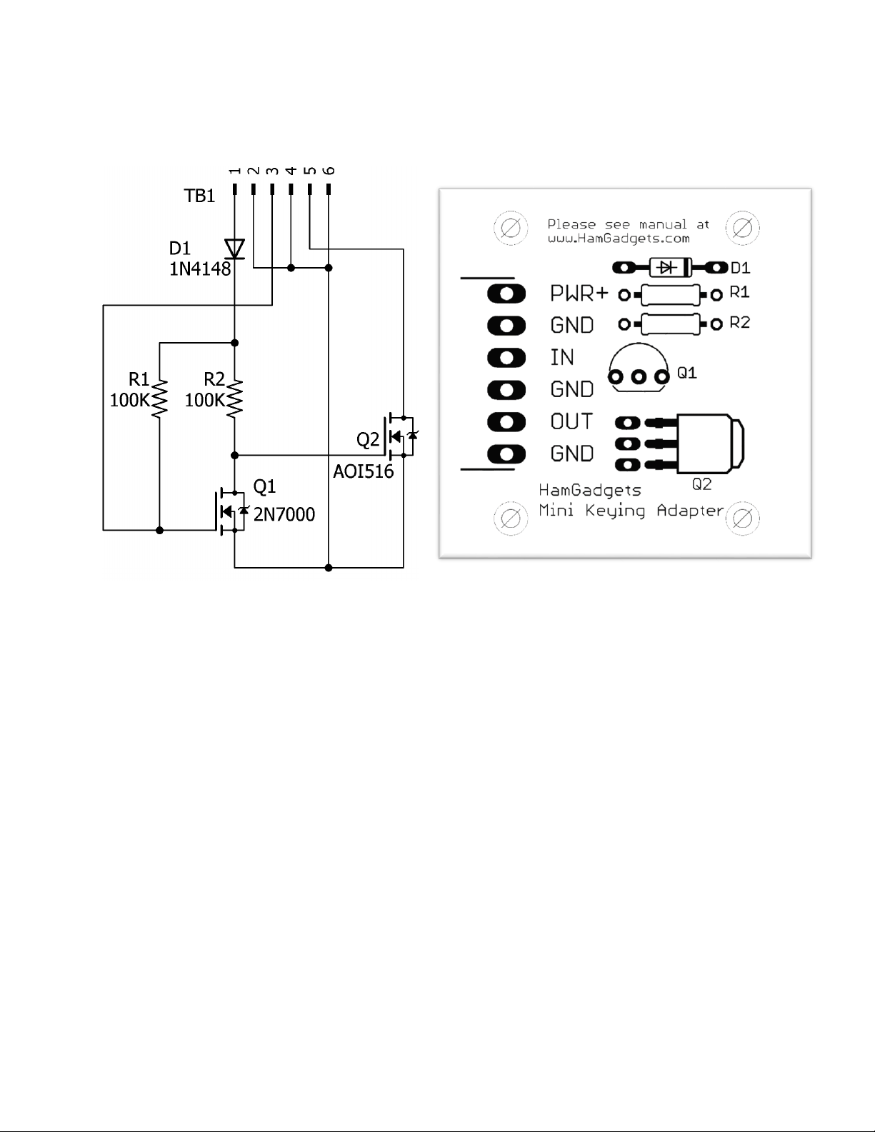
The Mini-KA needs three things to be useful: a source of DC power, input from your
keyer, and a connection to your transmitter.
Ground (GND): All three GND terminals are interconnected. If you use only one and
are keying a load of more than a few dozen mA, it’s best to use the GND terminal closest
to the bottom edge of the board. This has a much heavier trace and can carry more
current than the other two.
Power: Nominally 12 volts, but the power source can be any smooth, filtered DC power
source from 5 to 18 volts. It will probably be convenient to use the same DC power
source you use for your transmitter or transceiver. Don’t exceed 18 volts input, and make
sure you don’t reverse the power wires. They are very clearly marked PWR+ and GND.
Don’t use an AC power supply, or an unregulated DC power supply with no filtering.
Input: Input can be from any ON/OFF switched or keyed source. Usually this will be
your electronic keyer, such as the Ultra PicoKeyer. You can, however, use the Mini
Keying Adapter with a straight key, bug, some other electronic keyer, or even a computer
serial or parallel output signal. If your radio immediately starts transmitting when you
connect the keyer to the Mini Keying Adapter, you’ve probably got the IN/GND wires
reversed.
Output: Output is an ON/OFF keyed signal, the same as that from your electronic keyer.
Connect it to your transmitter or transceiver’s KEY input jack. If your radio immediately
starts transmitting when you connect the Mini Keying Adapter to the radio, you’ve
probably got the OUT/GND wires reversed.
CAUTION: There is no isolation between the power supply, keyer and transmitter.
Don’t use this circuit with high voltages, such as with grid-block or cathode keyed tube
gear. All grounds should be common –if you have things plugged into different outlets,

Mini Keying Adapter 01/07/2016 Page 5 of 6
power strips or house circuits, make sure you don’t have a floating ground or a high
resistance path somewhere. It’s not normally an issue, but I’m always surprised at how
we find new ways to break things.
Theory of Operation
In logic terms, the Mini Keying Adapter consists of two inverter/buffer stages.
The gate of MOSFET transistor Q1 is normally held high by resistor R1, keeping Q1
turned ON (conducting). Q1 presents a low resistance to ground, keeping the gate of Q2
near ground potential. In this state Q2 is turned OFF (not conducting). Q2 presents a
high impedance to the output, keeping the transmitter from transmitting.
When the gate of Q1 is driven low by the input signal, it stops conducting. The gate of
Q2 is then pulled high by R2, turning Q2 on. Q2 presents a low impedance to the output,
keying the transmitter.
Diode D1 attempts to prevent damage to the circuit by blocking the flow of current
should the power input be connected incorrectly.
Warranty
All parts in your kit are guaranteed against defects for one year from date of purchase. This
warranty does not cover damage due to incorrect assembly, improper soldering or wiring,
overvoltage, static damage or other misuse or abuse. If you have problems, please contact me via
email to arrange for an exchange or replacement part. If you accidentally damage a part, don’t
panic –just contact me, replacements are not expensive.
Specifications
Input power: 12V nominal, DC only, 5 –18 volt range
Input current: 0.2 mA max
Input voltage: -20 to +20 Volts absolute maximum
Input impedance: 100K Ohms (pull-up to supply voltage)
Output voltage: 30 V max
Output current: 2.5 A DC max continuous (may require additional cooling)
Output ON resistance: Less than 2 Ohms typical
Turn-On time Less than 1 microsecond
Turn-Off time Less than 1 microsecond

Mini Keying Adapter 01/07/2016 Page 6 of 6
Schematic and PCB Diagrams
This manual suits for next models
1
Table of contents
Other HamGadgets Adapter manuals