HELIX MxC 200 User manual

Helix Semiconductors, 2019 All Rights Reserved 1
1.30.19
MxC® 200 PoL EVB Manual
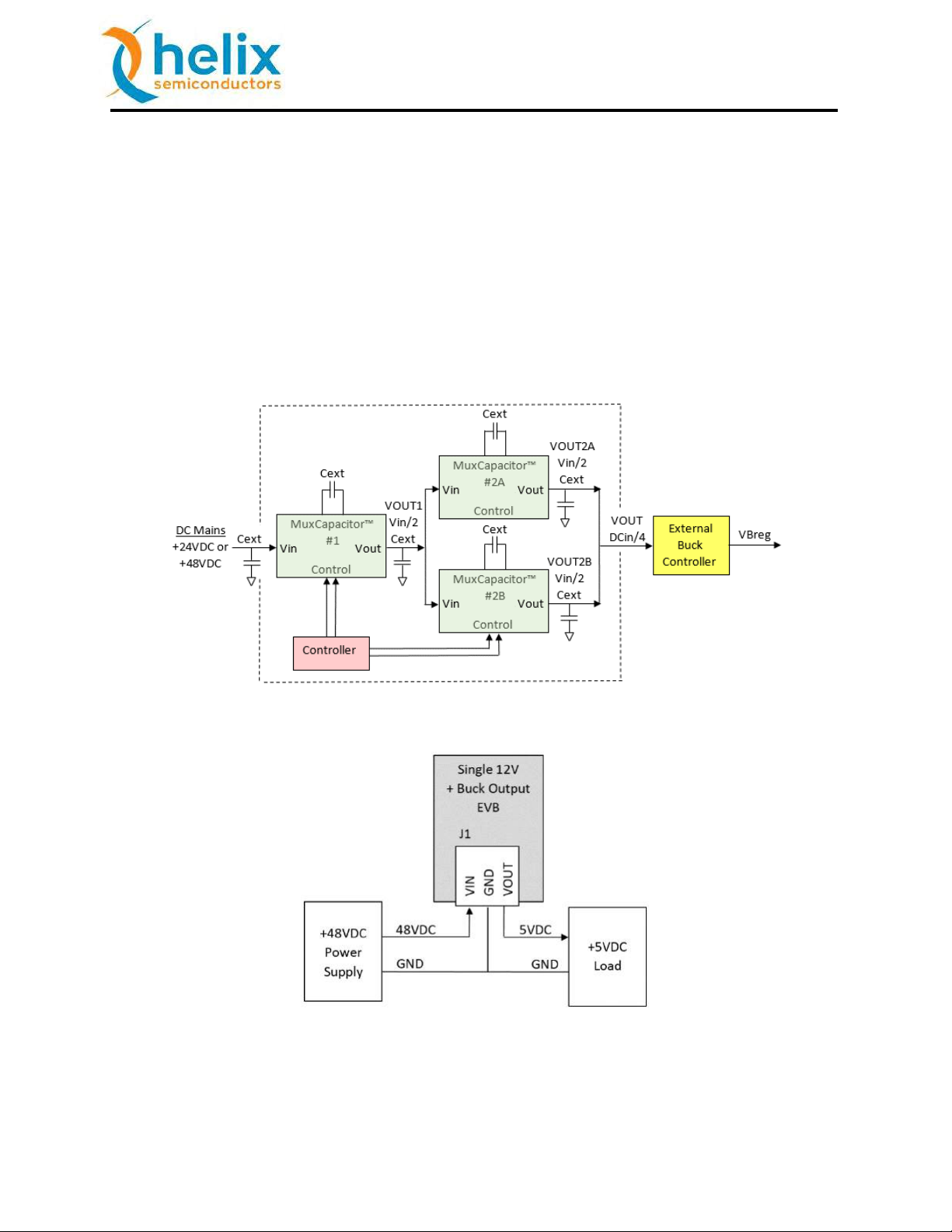
MxC® 200 Evaluation Boards
Helix Semiconductors offers four MxC 200
DC-DC PoL (Point of Load) Evaluation Board
configurations: Single 12V output, Triple
24V/12V/6V outputs, regulated 5V output
and a 4x voltage boost output. Additionally,
a voltage boost+LED driver is offered. Each
evaluation board is self- contained and
ready for use.
Wiring connection diagram, schematic and
BOM for each board are included in this
manual. Gerber files are available upon
request.
Target Applications
Telecom Blades, Data Centers
PoE: Wireless Access Points, Security
Cameras, VoIP Phones
Electric & Hybrid Automobiles
Industrial Controllers, HVAC
IoT & IIoT Gateways
Features
Four Configurations
oSingle 12V Output
oTriple 24V/12V/6V Outputs
oRegulated 5V Output
oVoltage Boost
15W Output (Multiple Outputs)
oPout = Pout1 + Pout2 + Pout3
Idle Operation: Active, No-Load
o1mW Non-Switching
o48mW Switching
> 97% Efficiency @ 2.6W
> 90% Efficiency @ 15W
Fault Detectors
oOutput Over Current
oThermal Shutdown
External Control Signals
oEnable
oExternal Clock Enable
oExternal Clock Input
Single 12V Output Triple 24/12/6V Outputs Regulated 5V Output
P/N: MxC 291-EB3-C P/N: MxC 290-EB9-C P/N: MxC 292-EB3-C

Helix Semiconductors, 2019 All Rights Reserved 2
1.30.19
MxC® 200 PoL EVB Manual
1. Table of Contents
1. Table of Contents..................................................................................................................... 2
2. Table of Figures ....................................................................................................................... 2
3. Table of Tables......................................................................................................................... 3
4. MxC 291 Single 12V Output EVB ............................................................................................. 4
5. MxC 290 Triple 24V/12V/6V Output EVB................................................................................ 8
6. MxC 292 +5V Buck Reg. Output EVB ..................................................................................... 13
7. MxC 281 4x Voltage Boost Output EVB................................................................................. 18
8. MxC 284 Voltage Boost with LED Current Source Output EVB ............................................. 22
9. Output Current Sharing ......................................................................................................... 26
10. Performance Data.................................................................................................................. 27
10.1. Operational Guidelines .................................................................................................. 27
11. Flying Capacitor Value Verses Efficiency ............................................................................... 28
2. Table of Figures
Figure 1: MxC 291 Single 12V Output EVB Block Diagram ............................................................. 4
Figure 2: MxC 291 Single 12V Output EVB Standalone Wiring Diagram ........................................ 4
Figure 3: MxC 291 Single 12V Output EVB SMPS Wiring Diagram ................................................. 5
Figure 4: MxC 291 Single 12V Output EVB Schematic .................................................................... 6
Figure 5: MxC 291 Single 12V Output EVB Efficiency Curve .......................................................... 7
Figure 6: MxC 290 Triple Output EVB Block Diagram..................................................................... 8
Figure 7: MxC 290 Triple Output EVB Standalone Wiring Diagram................................................ 8
Figure 8: MxC 290 Triple Output Evaluation Board Synchronized to SMPS Wiring Diagram......... 9
Figure 9: MxC 290 Triple 24V/12V/6V Output EVB Schematic..................................................... 11
Figure 10: MxC 290 Triple 24V/12V/6V Output EVB Efficiency Curve ......................................... 12
Figure 11: MxC 292 +5V Buck Reg. Output EVB Block Diagram ................................................... 13
Figure 12: MxC 292 +5V Buck Reg. Output EVB Standalone Wiring Diagram.............................. 13
4x Voltage Boost Output 4x Voltage Boost + LED
P/N: MxC 281-EB3-C P/N: MxC 284-EB2-C

Helix Semiconductors, 2019 All Rights Reserved 3
1.30.19
MxC® 200 PoL EVB Manual
Figure 13: MxC 292 +5V Buck Reg. Output EVB Schematic .......................................................... 16
Figure 14: MxC 292 w/Synchronous 5V Buck Reg. Output EVB Schematic.................................. 16
Figure 15: MxC 292 w/Synchronous Buck 5V Output EVB Efficiency Curve ................................ 17
Figure 16: MxC 281 4x Voltage Boost Output EVB Block Diagram ............................................... 18
Figure 17: MxC 281 4x Voltage Boost Output EVB Standalone Wiring Diagram.......................... 18
Figure 18: MxC 281 4x Voltage Boost Output EVB Schematic...................................................... 21
Figure 19: MxC 281 4x Voltage Boost Output EVB Efficiency Curve ............................................ 21
Figure 20: MxC 284 4x Voltage Boost + LED EVB Block Diagram.................................................. 22
Figure 21: MxC 284 4x Voltage Boost + LED EVB Standalone Wiring Diagram ............................ 22
Figure 22: MxC 284 4x Voltage Boost + LED EVB Schematic ........................................................ 25
Figure 23: MxC 284 4x Voltage Boost with LED Back Panel ......................................................... 25
Figure 24: MxC 291 Output Current Sharing 120W 48V-to-12V Voltage Converter.................... 26
Figure 25: Efficiency Measurement Wiring Diagram.................................................................... 27
Figure 26: Typical Capacitance verses DC Bias, 50V Device ......................................................... 28
3. Table of Tables
Table 1: MxC 291 Single 12V Output EVB Connector –J1.............................................................. 5
Table 2: MxC 291 Single 12V Output EVB Bill of Materials (BOM)................................................. 6
Table 3: MxC 290 Triple 24V/12V/6V Output EVB Connector –J1............................................... 10
Table 4: MxC 290 Triple 24V/12V/6V Output EVB Bill of Materials (BOM).................................. 12
Table 5: MxC 292 +5V Buck Reg. Output EVB Connector –J1...................................................... 14
Table 6: MxC 292 +5V Buck Reg. Output EVB Bill of Materials (BOM)......................................... 15
Table 7: MxC 281 4x Voltage Boost Output EVB Connector –J1 ................................................. 19
Table 8: MxC 281 4x Voltage Boost Output EVB Bill of Materials (BOM) .................................... 20
Table 9: MxC 284 4x Voltage Boost + LED Output EVB Connector –J1........................................ 23
Table 10: MxC 284 4x Voltage Boost + LED Output EVB Bill of Materials (BOM)......................... 24
Table 11: Revision History............................................................................................................. 29

Helix Semiconductors, 2019 All Rights Reserved 4
1.30.19
MxC® 200 PoL EVB Manual
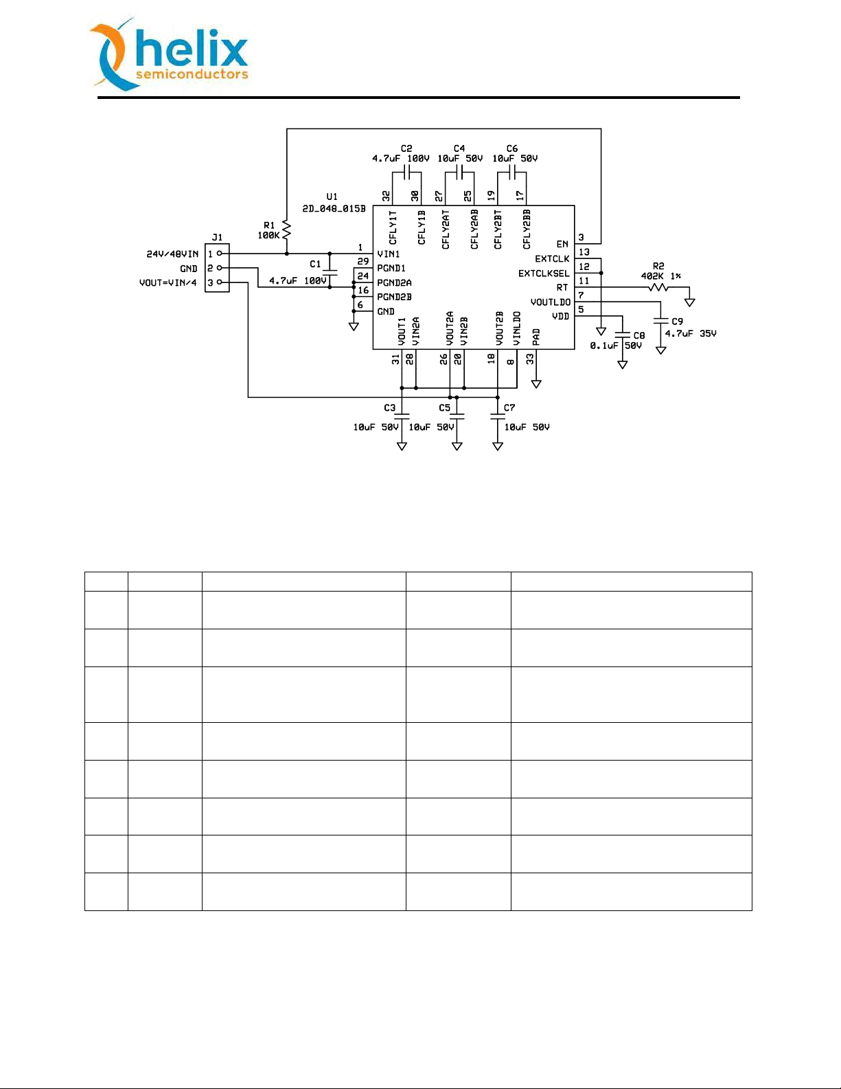
4. MxC 291 Single 12V Output EVB
The MxC 291-EB3-C Single 12V Output EVB can be operated as a standalone Divide-By-4 voltage
reducer or synchronized with a SMPS. The EVB utilizes the 2D_048_015B MxC 200 family
device.
When the MxC 291 is providing power to a SMPS, the synchronization feature of the
2D_048_015B allows the MuxCapacitor switching to slow down as the SMPS enters pulse
skipping. This operation reduces switching power losses at no-load to light-load conditions. The
EXTCLK can be provided by either a FET gate drive signal or a buck regulator’s switched output.
Both the EXTCLKSEL and EXTCLK inputs accept up to 30V signals.
The MxC 291 Single 12V Output EVB provides the highest efficiency 12 Volt output
configuration.
Figure 1: MxC 291 Single 12V Output EVB Block Diagram

Helix Semiconductors, 2019 All Rights Reserved 5
1.30.19
MxC® 200 PoL EVB Manual
Figure 2: MxC 291 Single 12V Output EVB Standalone Wiring Diagram
Warning: Do not “Hot-Plug” the power supply or electronic load.
Recommended start-up procedure:
1) With power supply off, attach power supply wires.
2) With electronic load disabled (monitor mode), attach electronic load wires.
3) Turn on power supply.
4) Enable electronic load with no load current, and then ramp up load current.
Figure 3: MxC 291 Single 12V Output EVB SMPS Wiring Diagram
Table 1: MxC 291 Single 12V Output EVB Connector –J1
Pin No.
Name
Description
1
VIN
+48VDC Input Power Pin
2
GND
Power GND Pin
3
VOUT
+12VDC Output Power Pin
Note:
1) Due to board’s small size, thermal dissipation is limited and may exceed the over-
temperature shutdown threshold.
2) The MxC 291 can be powered from 24V delivering 6Vout.
Helix Semiconductors, 2019 All Rights Reserved 6
1.30.19
MxC® 200 PoL EVB Manual
Figure 4: MxC 291 Single 12V Output EVB Schematic
Table 2: MxC 291 Single 12V Output EVB Bill of Materials (BOM)
Qty
Ref. No.
Description
Package
Manufacturer
1
C8
CAP, 0.1µF±10%, 50V
0603
1608 Metric
Wurth Elektronik
WCAP-CSGP 885012206095
1
C9
CAP, 4.7µF±10%, 35V
0603
1608 Metric
TDK
C1608X5R1V475M080AC
5
C3, C4,
C5, C6,
C7
CAP, 10µF±10%, 50V
1210
3225 Metric
TDK
C3225X7S1H106M250AB
2
C1, C2
CAP, 4.7µF±10%, 100V
1210
3225 Metric
TDK
C3225X7S2A475M200AB
1
R1
RES, 100KΩ±10%
0603
1608 Metric
Rohm
ESR03EZPJ104
1
R2
RES, 402 KΩ±1%
0603
1608 Metric
Rohm
MCR03ERTF4023
1
U1
IC, 2D_048_015B, QFN5x5,
32P 0.5
QFN32
Helix Semiconductors
2D-048-015B-QFN32-C
1
J1
CONN, 6P, M, R/A, 0.100
SIP100P6
Wurth Elektronik
WR-PHD 61300611021
Helix Semiconductors, 2019 All Rights Reserved 7
1.30.19
MxC® 200 PoL EVB Manual
Figure 5: MxC 291 Single 12V Output EVB Efficiency Curve
Helix Semiconductors, 2019 All Rights Reserved 8
1.30.19
MxC® 200 PoL EVB Manual
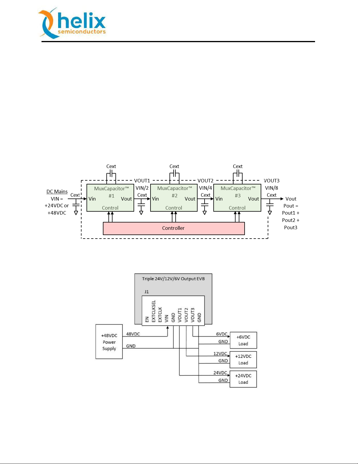
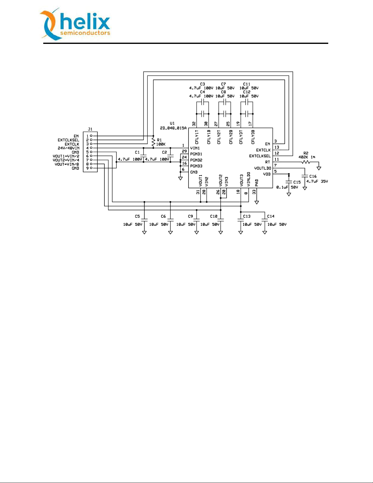
5. MxC 290 Triple 24V/12V/6V Output EVB
The MxC 290-EB9-C Triple 24V/12V/6V Output EVB can be operated as a standalone fixed
frequency voltage reducer or synchronized with a SMPS. The EVB utilizes the 2D_048_015A
MxC 200 family device.
When the MxC 290 is providing power to a SMPS, the synchronization feature of the
2D_048_015A allows the MuxCapacitor switching to slow down as the SMPS enters pulse
skipping. This operation reduces switching power losses at no-load to light-load conditions. The
EXTCLK can be provided by either a FET gate drive signal or a buck regulator’s switched output.
Both the EXTCLKSEL and EXTCLK inputs accept up to 30V signals.
Figure 6: MxC 290 Triple Output EVB Block Diagram
Figure 7: MxC 290 Triple Output EVB Standalone Wiring Diagram

Helix Semiconductors, 2019 All Rights Reserved 9
1.30.19
MxC® 200 PoL EVB Manual
Figure 8: MxC 290 Triple Output Evaluation Board Synchronized to SMPS Wiring Diagram
Warning: Do not “Hot-Plug” the power supply or electronic load.
Recommended start-up procedure:
1) With power supply off, attach power supply wires.
2) With electronic load disabled (monitor mode), attach electronic load wires.
3) Turn on power supply.
4) Enable electronic load with no load current, and then ramp up load current.
Helix Semiconductors, 2019 All Rights Reserved 10
1.30.19
MxC® 200 PoL EVB Manual
Table 3: MxC 290 Triple 24V/12V/6V Output EVB Connector –J1
Pin No.
Name
Description
1
EN
Device Enable: Input Pin, On-board 100KΩ Pull-Up, 60Vmax
0 = Disable, 1 = Enable
2
EXTCLKSEL
External Clock Sync Enable: Input Pin, Internal 2MΩ Pull-Down,
30Vmax
0 = Internal Clock, 1 = External Clock
3
EXTCLK
External Clock Sync: Input pin, Internal 2MΩ Pull-Down, 30Vmax
4
VIN
+48VDC Input Power Pin
5
GND
Power GND Pin
6
24VOUT
+24VDC Output Power Pin, See Note 2.
7
12VOUT
+12VDC Output Power Pin, See Note 2.
8
6VOUT
+6VDC Output Power Pin, See Note 2.
9
GND
Power GND Pin
Note:
1) Maximum thermal dissipation occurs when high currents are drawn from 6VOUT. Due
to board’s small size, thermal dissipation is limited and may exceed the over-
temperature shutdown threshold.
2) The 24VOUT output provides 0.5A and 12VOUT/6VOUT outputs provide 1A. Actual
delivered power depends on the output voltage of each stage.
3) The MxC 290 can be powered from 24V delivering one-half the output voltage at pins 6-
8 as stated in Table 3.
Helix Semiconductors, 2019 All Rights Reserved 11
1.30.19
MxC® 200 PoL EVB Manual
Figure 9: MxC 290 Triple 24V/12V/6V Output EVB Schematic

Helix Semiconductors, 2019 All Rights Reserved 12
1.30.19
MxC® 200 PoL EVB Manual
Table 4: MxC 290 Triple 24V/12V/6V Output EVB Bill of Materials (BOM)
Qty
Ref. No.
Description
Package
Manufacturer
1
C15
CAP, 0.1µF±10%, 10V
0603
1608 Metric
Wurth Elektronik
WCAP-CSGP 885012206095
1
C16
CAP, 4.7µF±10%, 35V
0603
1608 Metric
TDK
C1608X5R1V475M080AC
10
C5, C6, C7,
C8, C9, C10,
C11, C12,
C13, C14
CAP, 10µF±10%, 50V
1210
3225 Metric
TDK
C3225X7S1H106M250AB
4
C1, C2, C3,
C4
CAP, 4.7µF±10%, 100V
1210
3225 Metric
TDK
C3225X7S2A475M200AB
1
R1
RES, 100KΩ±10%
0603
1608 Metric
Rohm
ESR03EZPJ104
1
R2
RES, 402 KΩ±1%
0603
1608 Metric
Rohm
MCR03ERTF4023
1
U1
IC, 2D_048_015A, QFN5x5,
32P 0.5
QFN32
Helix Semiconductors
2D-048-015A-QFN32-C
1
J1
CONN, 9P, M, R/A, 0.100
SIP100P9
Wurth Elektronik
WR-PHD 61300911021
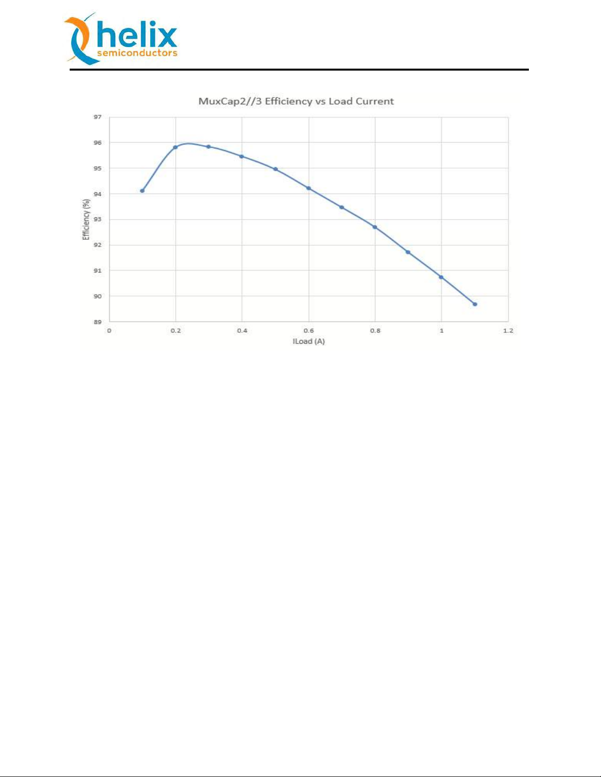
Figure 10: MxC 290 Triple 24V/12V/6V Output EVB Efficiency Curve
Helix Semiconductors, 2019 All Rights Reserved 13
1.30.19
MxC® 200 PoL EVB Manual
6. MxC 292 +5V Buck Reg. Output EVB
The MxC 292-EB3-C +5V Buck Reg. Output EVB can be operated as a standalone regulated 5V
output board. The EVB utilizes the 2D_048_015B MxC 200 family device.
When the MxC 292 is providing power to another SMPS, the synchronization feature of the
2D_048_015B allows the MuxCapacitor switching to slow down as the SMPS enters pulse
skipping. This operation reduces switching power losses at no-load to light-load conditions. The
EXTCLK can be provided by either a FET gate drive signal or a buck regulator’s switched output
to enhance light-load efficiency. Both the EXTCLKSEL and EXTCLK inputs accept up to 30V
signals.
Figure 11: MxC 292 +5V Buck Reg. Output EVB Block Diagram
Figure 12: MxC 292 +5V Buck Reg. Output EVB Standalone Wiring Diagram

Helix Semiconductors, 2019 All Rights Reserved 14
1.30.19
MxC® 200 PoL EVB Manual
Warning: Do not “Hot-Plug” the power supply or electronic load.
Recommended start-up procedure:
1) With power supply off, attach power supply wires.
2) With electronic load disabled (monitor mode), attach electronic load wires.
3) Turn on power supply.
4) Enable electronic load with no load current, and then ramp up load current.
Table 5: MxC 292 +5V Buck Reg. Output EVB Connector –J1
Pin No.
Name
Description
1
VIN
+48VDC Input Power Pin
2
GND
Power GND Pin
3
VOUT
+5VDC Output Power Pin
Note:
1) Due to board’s small size, thermal dissipation is limited and may exceed the over-
temperature shutdown threshold.
2) The MxC 292 can be powered from 24V delivering 6V to the buck regulator. The
minimum VIN for the TPS565201 is 4.5V.
3) Other buck regulator output voltages are available by changing R4. Refer to the VOUT
Table in Figures 13 and 14.

Helix Semiconductors, 2019 All Rights Reserved 15
1.30.19
MxC® 200 PoL EVB Manual
Table 6: MxC 292 +5V Buck Reg. Output EVB Bill of Materials (BOM)
Qty
Ref. No.
Description
Package
Manufacturer
1
C8
CAP, 0.1µF±10%, 50V
0603
1608 Metric
Wurth Elektronik
WCAP-CSGP 885012206095
1
C9
CAP, 4.7µF±10%, 35V
0603
1608 Metric
TDK
C1608X5R1V475M080AC
5
C3, C4, C5,
C6, C7
CAP, 10µF±10%, 50V
1210
3225 Metric
TDK
C3225X7S1H106M250AB
3
C1, C2A,
C2B
CAP, 4.7µF±10%, 100V
1210
3225 Metric
TDK
C3225X7S2A475M200AB
1
R1
RES, 100KΩ±10%
0603
1608 Metric
Rohm
ESR03EZPJ104
1
R2
RES, 402KΩ±1%
0603
1608 Metric
Rohm
MCR03ERTF4023
1
U1
IC, 2D_048_015B, QFN5x5,
32P 0.5
QFN32
Helix Semiconductors
2D-048-015B-QFN32-C
1
J1
CONN, 3P, M, R/A, 0.100
SIP100P3
Wurth Elektronik
WR-PHD 61300611021
1
C10
CAP, 1µF±10%, 16V
0603
1608 Metric
Wurth Elektronik
WCAP-CSGP 885012106017
1
C11
CAP, 0.1µF±10%, 25V
0603
1608 Metric
Wurth Elektronik
WCAP-CSGP 885012206071
2
C12, C13
CAP, 22µF±10%, 35V
1206
3216 Metric
TDK
C3216X5R1V226M160AC
1
R3
RES, 100KΩ
0603
1608 Metric
Rohm
ESR03EZPJ104
1
R4
RES, 54.9KΩ±1%
0603
1608 Metric
Rohm
MCR03ERTF5493
1
R5
RES, 10.0KΩ±1%
0603
1608 Metric
Rohm
MCR03ERTF1003
1
L1
IND, 4.7uH, 9A
PG0642
Wurth Elektronik
WR-LHMI 74437349047
1
U2
IC, TPS565201
TSOP8
TI
TPS565201D
Helix Semiconductors, 2019 All Rights Reserved 16
1.30.19
MxC® 200 PoL EVB Manual
Figure 13: MxC 292 +5V Buck Reg. Output EVB Schematic
Figure 14: MxC 292 w/Synchronous 5V Buck Reg. Output EVB Schematic

Helix Semiconductors, 2019 All Rights Reserved 17
1.30.19
MxC® 200 PoL EVB Manual
Sync
Non-Sync
65.0
70.0
75.0
80.0
85.0
90.0
95.0
0 0.5 1 1.5 2 2.5
Efficiency (%)
Iload (A)
Non-Synchronous & Synchronous Efficiency
vs Load Current
Sync
Non-
Sync
70.0
75.0
80.0
85.0
90.0
95.0
0 0.05 0.1
Efficiency (%)
ILoad (A)
Light Load
Efficiency Sync vs
Non-Sync
Figure
15: MxC
292
w/Synchronous
Buck 5V Output
EVB Efficiency
Curve
Helix Semiconductors, 2019 All Rights Reserved 18
1.30.19
MxC® 200 PoL EVB Manual
7. MxC 281 4x Voltage Boost Output EVB
The MxC 281-EB3-C 4x Voltage Boost Output EVB can be operated as a standalone fixed
frequency voltage boost or synchronized with a SMPS. The EVB utilizes the 2U_012_010A MxC
200 family device.
When the MxC 281 is providing power to a SMPS, the synchronization feature of the
2U_012_010A allows the MuxCapacitor switching to slow down as the SMPS enters pulse
skipping. Refer to Section 6 for enabling the synchronization operation.
The input voltage range is 6V to 12V for an output voltage range of 24V to 48V, respectively.
Figure 16: MxC 281 4x Voltage Boost Output EVB Block Diagram
Figure 17: MxC 281 4x Voltage Boost Output EVB Standalone Wiring Diagram
Helix Semiconductors, 2019 All Rights Reserved 19
1.30.19
MxC® 200 PoL EVB Manual
Warning: Do not “Hot-Plug” the power supply or electronic load.
Recommended start-up procedure:
1) With power supply off, attach power supply wires.
2) With electronic load disabled (monitor mode), attach electronic load wires.
3) Turn on power supply.
4) Enable electronic load with no load current, and then ramp up load current.
Table 7: MxC 281 4x Voltage Boost Output EVB Connector –J1
Pin No.
Name
Description
1
VIN
+12VDC Input Power Pin
2
GND
Power GND Pin
3
VOUT
+48VDC Output Power Pin
Note:
1) Due to board’s small size, thermal dissipation is limited and may exceed the over-
temperature shutdown threshold.
2) The MxC 281 can be powered from 6V to 12V delivering 24V to 48V, respectively to the
load.

Helix Semiconductors, 2019 All Rights Reserved 20
1.30.19
MxC® 200 PoL EVB Manual
Table 8: MxC 281 4x Voltage Boost Output EVB Bill of Materials (BOM)
Qty
Ref. No.
Description
Package
Manufacturer
1
C8
CAP, 0.1µF±10%, 50V
0603
1608 Metric
Wurth Elektronik
WCAP-CSGP 885012206095
1
C9
CAP, 4.7µF±10%, 35V
0603
1608 Metric
TDK
C1608X5R1V475M080AC
5
C3, C4, C5,
C6, C7
CAP, 10µF±10%, 50V
1210
3225 Metric
TDK
C3225X7S1H106M250AB
3
C1, C2
CAP, 4.7µF±10%, 100V
1210
3225 Metric
TDK
C3225X7S2A475M200AB
1
R1
RES, 100KΩ±10%
0603
1608 Metric
Rohm
ESR03EZPJ104
1
R2
RES, 402KΩ±1%
0603
1608 Metric
Rohm
MCR03ERTF4023
1
U1
IC, 2U_012_010A, QFN5x5,
32P 0.5
QFN32
Helix Semiconductors
2U-012-010A-QFN32-C
1
J1
CONN, 3P, M, R/A, 0.100
SIP100P3
Wurth Elektronik
WR-PHD 61300611021
Other manuals for MxC 200
1
This manual suits for next models
5
Table of contents
Other HELIX Motherboard manuals


Popular Motherboard manuals by other brands

Gigabyte
Gigabyte GA-M52LT-D3 user manual

SMSC
SMSC PCM-2074 user manual

ECS
ECS A55F-M3 manual

SHENZHEN ANHUA OPTOELECTRONICS TECHNOLOGY
SHENZHEN ANHUA OPTOELECTRONICS TECHNOLOGY H6 user guide

IBASE Technology
IBASE Technology MI997AF user manual

Texas Instruments
Texas Instruments PCM1802EVM user guide


