Hitachi H8S/2646 User manual

Hitachi 16-Bit Single-Chip Microcomputer
H8S/2646 Series
H8S/2646
HD6432646
H8S/2645
HD6432645
H8S/264
HD643264
H8S/2648
HD6432648
H8S/2646R F-ZTAT™
HD64F2646R
H8S/2648R F-ZTAT™
HD64F2648R
Hardware Manual
ADE-602-20 C
Rev. 4.0
9/20/02
Hitachi, Ltd.

Cautions
1. Hitachi neither warrants nor grants licenses of any rights of Hitachi’s or any third party’s
patent, copyright, trademark, or other intellectual property rights for information contained in
this document. Hitachi bears no responsibility for problems that may arise with third party’s
rights, including intellectual property rights, in connection with use of the information
contained in this document.
2. Products and product specifications may be subject to change without notice. Confirm that you
ha e recei ed the latest product standards or specifications before final design, purchase or
use.
3. Hitachi makes e ery attempt to ensure that its products are of high quality and reliability.
Howe er, contact Hitachi’s sales office before using the product in an application that
demands especially high quality and reliability or where its failure or malfunction may directly
threaten human life or cause risk of bodily injury, such as aerospace, aeronautics, nuclear
power, combustion control, transportation, traffic, safety equipment or medical equipment for
life support.
4. Design your application so that the product is used within the ranges guaranteed by Hitachi
particularly for maximum rating, operating supply oltage range, heat radiation characteristics,
installation conditions and other characteristics. Hitachi bears no responsibility for failure or
damage when used beyond the guaranteed ranges. E en within the guaranteed ranges,
consider normally foreseeable failure rates or failure modes in semiconductor de ices and
employ systemic measures such as fail-safes, so that the equipment incorporating Hitachi
product does not cause bodily injury, fire or other consequential damage due to operation of
the Hitachi product.
5. This product is not designed to be radiation resistant.
6. No one is permitted to reproduce or duplicate, in any form, the whole or part of this document
without written appro al from Hitachi.
7. Contact Hitachi’s sales office for any questions regarding this document or Hitachi
semiconductor products.

General Precautions on the Handling of Products
1. Treatment of NC Pins
Note: Do not connect anything to the NC pins.
The NC (not connected) pins are either not connected to any of the internal circuitry or are
used as test pins or to reduce noise. If something is connected to the NC pins, the
operation of the LSI is not guaranteed.
2. Treatment of Unused Input Pins
Note: Fix all unused input pins to high or low le el.
Generally, the input pins of CMOS products are high-impedance input pins. If unused pins
are in their open states, intermediate le els are induced by noise in the icinity, a pass-
through current flows internally, and a malfunction may occur.
3. Processing before Initialization
Note: When power is first supplied, the product’s state is undefined. The states of internal
circuits are undefined until full power is supplied throughout the chip and a low le el is
input on the reset pin. During the period where the states are undefined, the register
settings and the output state of each pin are also undefined. Design your system so that it
does not malfunction because of processing while it is in this undefined state. For those
products which ha e a reset function, reset the LSI immediately after the power supply has
been turned on.
4. Prohibition of Access to Undefined or Reser ed Address
Note: Access to undefined or reser ed addresses is prohibited.
The undefined or reser ed addresses may be used to expand functions, or test registers
may ha e been be allocated to these address. Do not access these registers: the system’s
operation is not guaranteed if they are accessed.


Preface
The H8S/2646 Series is a series of high-performance microcontrollers with a 32-bit H8S/2600
CPU core, and a set of on-chip supporting functions required for system configuration.
This LSI is equipped with a 16-bit timer pulse unit (TPU), programmable pulse generator (PPG),
watchdog timer (WDT), serial communication interface (SCI), A/D con erter, motor control
PWM timer (PWM), LCD controller/dri er (LCDC) and I/O ports as on-chip supporting modules.
In addition, data transfer controller (DTC) is pro ided, enabling high-speed data transfer without
CPU inter ention. This LSI is suitable for use as an embedded processor for high-le el control
systems. Its on-chip ROM are flash memory (F-ZTAT™*) that pro ides flexibility as it can be
reprogrammed in no time to cope with all situations from the early stages of mass production to
full-scale mass production. This is particularly applicable to application de ices with
specifications that will most probably change.
Note: * F-ZTAT™ is a trademark of Hitachi, Ltd.
Target Users: This manual was written for users who will be using the H8S/2646 Series in the
design of application systems. Members of this audience are expected to understand
the fundamentals of electrical circuits, logical circuits, and microcomputers.
Objecti e: This manual was written to explain the hardware functions and electrical
characteristics of the H8S/2646 Series to the abo e audience. Refer to the
H8S/2600 Series, H8S/2000 Series Programming Manual for a detailed description
of the instruction set.
Notes on reading this manual:
• In order to understand the o erall functions of the chip
Read the manual according to the contents. This manual can be roughly categorized into parts
on the CPU, system control functions, peripheral functions and electrical characteristics.
• In order to understand the details of the CPU's functions
Read the H8S/2600 Series, H8S/2000 Series Programming Manual.
• In order to understand the details of a register when its name is known
The addresses, bits, and initial alues of the registers are summarized in Appendix B, Internal
I/O Registers.
Example: Bit order: The MSB is on the left and the LSB is on the right.
Related Manuals: The latest ersions of all related manuals are a ailable from our web site.
Please ensure you ha e the latest ersions of all documents you require.
http://www.hitachisemiconductor.com/
H8S/2646 Series manuals:
Manual Title ADE No.
H8S/2646 Series Hardware Manual This manual
H8S/2600 Series, H8S/2000 Series Programming Manual ADE-602-08
Users manuals for de elopment tools:
Manual Title ADE No.
C/C++ Complier, Assembler, Optimized Linkage Editor User's Manual ADE-702-247
Simulator Debugger (for Windows) Users Manual ADE-702-0 7
Hitachi Embedded Workshop Users Manual ADE-702-201
Application Notes:
Manual Title ADE No.
H8S Series Technical Q & A ADE-502-059

List of Items Revised or Added for This Version
Section Page Description
2.10.2 Caution to
observe when using
bit manipulation
instructions
76, 77 Newly added
The SET, CLR, NOT, ST and IST instructions read data in a unit of byte,
then, after bit manipulation, they write data in a unit of byte. Therefore, caution
must be exercised when executing any of these instructions for registers and
ports that include write-only bits.
The CLR instruction can be used to clear the flag of an internal I/O register to
0. In that case, if it is clearly known that the pertinent flag is set to 1 in an
interrupt processing routine or other processing, there is no need to read the
flag in advance.
8.3.10 Number of
DTC Execution States 207 4th line changed as follows
Number of execution states = I · (SI +1) + Σ (J · SJ + K · SK + L · SL) + M · SM
For example, when the DTC vector address table is located in on-chip ROM,
normal mode is set, and data is transferred from the on-chip ROM to an internal
I/O register, the time required for the DTC operation is 14 states. The time from
activation to the end of the data write is 11 states.
9.4.2 Register
Configuration
Table 9-6 Port 3
Register
Configuration
242
Name Abbreviation R/W Initial Value Address*
Port 3 data direction register P3DDR W H'00 H'FE32
Port 3 data register P3DR R/W H'00 H'FF02
Port 3 register PORT3 R Undefined H'FF 2
Port 3 open drain control register P3ODR R/W H'00 H'FE46
9.9.2 Register
Configuration 263 15th line changed as follows
In mode 7, if a pin is in the input state in accordance with the settings in the
DDR, setting the corresponding P PCR bit to 1 turns on the MOS input pull-up
for that pin.
9.10.3 Pin Functions
Table 9-20 Port C
Pin Functions
269 (Incorrect)PCDDR
(Correct)PCnDDR
9.13.1 Overview
Figure 9-12 Port F
Pin Functions
281
PF7 (input) / ø (output)
PF6 (I/O) / AS (output) / SEG20 (output) / SEG36* (output)
PF5 (I/O) / RD (output) / SEG19 (output) / SEG35* (output)
Pin functions in modes 4 to 6

Section Page Description
9.13.2 Register
Configuration 283 Part F Data Register (PFDR)
Bit:7654321
—PF6DR PF5DR PF4DR PF3DR PF2DR —PF DR
Initial value :
undefined
R/W : R/W R/W R/W R/W R/W R/W —R/W
2nd line changed as follows
PFDR is an 8-bit readable/writable register that stores output data for the port F
pins (PF6 to PF2, PF ).
6th line changed as follows
Bits 7 and 1 in PFDR are reserved, and only may be written to it.
15.2.3 Bit
Configuration
Register (BCR)
539 Figure of Detailed Description of Timing within 1 Bit, HCAN bit rate calculation,
BCR Setting Constraints, Table of Setting Range for TSEG1 and TSEG2 in
BCR
Moved to Bit Rate and Bit Timing Settings in section 15.3.2, Initialization after
Hardware Reset.
15.2.11 Interrupt
Register (IRR) 547 Bit 15—Overload Frame Interrupt Flag: Status flag indicating that the HCAN
has transmitted an overload frame.
Bit 15: IRR7 Description
[Clearing condition]
Writing 1 (Initial value)
1 Overload frame transmission
[Setting conditions]
When overload frame is transmitted
15.2.16 Unread
Message Status
Register (UMSR)
555 Bit table amended and Note added
UMSR
Bit: 15 14 13 12 11 1 9 8
UMSR7 UMSR6 UMSR5 UMSR4 UMSR3 UMSR2 UMSR1 UMSR
Initial value:
R/W: R/(W)*R/(W)*R/(W)*R/(W)*R/(W)*R/(W)*R/(W)*R/(W)*
Bit:7654321
UMSR15 UMSR14 UMSR13 UMSR12 UMSR11 UMSR1 UMSR9 UMSR8
Initial value:
R/W: R/(W)*R/(W)*R/(W)*R/(W)*R/(W)*R/(W)*R/(W)*R/(W)*
Note: *Only 1 can be written, to clear the flag.

Section Page Description
15.3.2 Initialization
after Hardware
Reset
it Rate and it
Timing Settings
565 to
567
it Rate and it Timing Settings: As bit rate settings, a baud rate setting and bit timing
setting must be made each time a CAN node begins communication. The baud rate and
bit timing settings are made in the bit configuration register ( CR).
Note: CR can be written to at all times, but should only be modified in configuration mode.
Settings should be made so that all CAN controllers connected to the CAN bus have the
same baud rate and bit width.
Refer to table 15.3 for the range of values that can be used as settings (TSEG1, TSEG2,
RP, sample point, and SJW) for CR.
Table 15-3 CR Register Value Setting Ranges
Name Abbreviation Min.
Value Max.
Value
Time segment 1 TSEG1 '0011 '1111
Time segment 2 TSEG2 '001 '111
aud rate prescaler RP '000000 '111111
Sample point SAM '0 '1
Re-synchronization jump width SJW '00 '11
Value Setting Ranges
• The value of SJW is stipulated in the CAN specifications.
3 ≥ SJW ≥ 0
• The minimum value of TSEG1 is stipulated in the CAN specifications.
TSEG1 > TSEG2
• The minimum value of TSEG2 is stipulated in the CAN specifications.
TSEG2 ≥ SJW
The following formula is used to calculate the baud rate.
f
CLK
2 × ( RP + 1) × (3 + TSEG1 + TSEG2)
it rate =
Note: f
CLK
= φ (system clock)
The CR value is used in the RP, TSEG1, and TSEG2.

Section Page Description
15.3.2 Initialization
after Hardware
Reset
it Rate and it
Timing Settings
565 to
567
Example: With a 1 Mb/s baud rate and a 20 MHz input clock:
20 MHz
2 × (0 + 1) × (3 + 4 + 3)
1 Mb/s =
Set Values Actual Values
f
CLK
= 20 MHz —
RP = 0 ( '000000) System clock × 2
TSEG1 = 4 ( '0100) 5TQ
TSEG2 = 3 ( '011) 4TQ
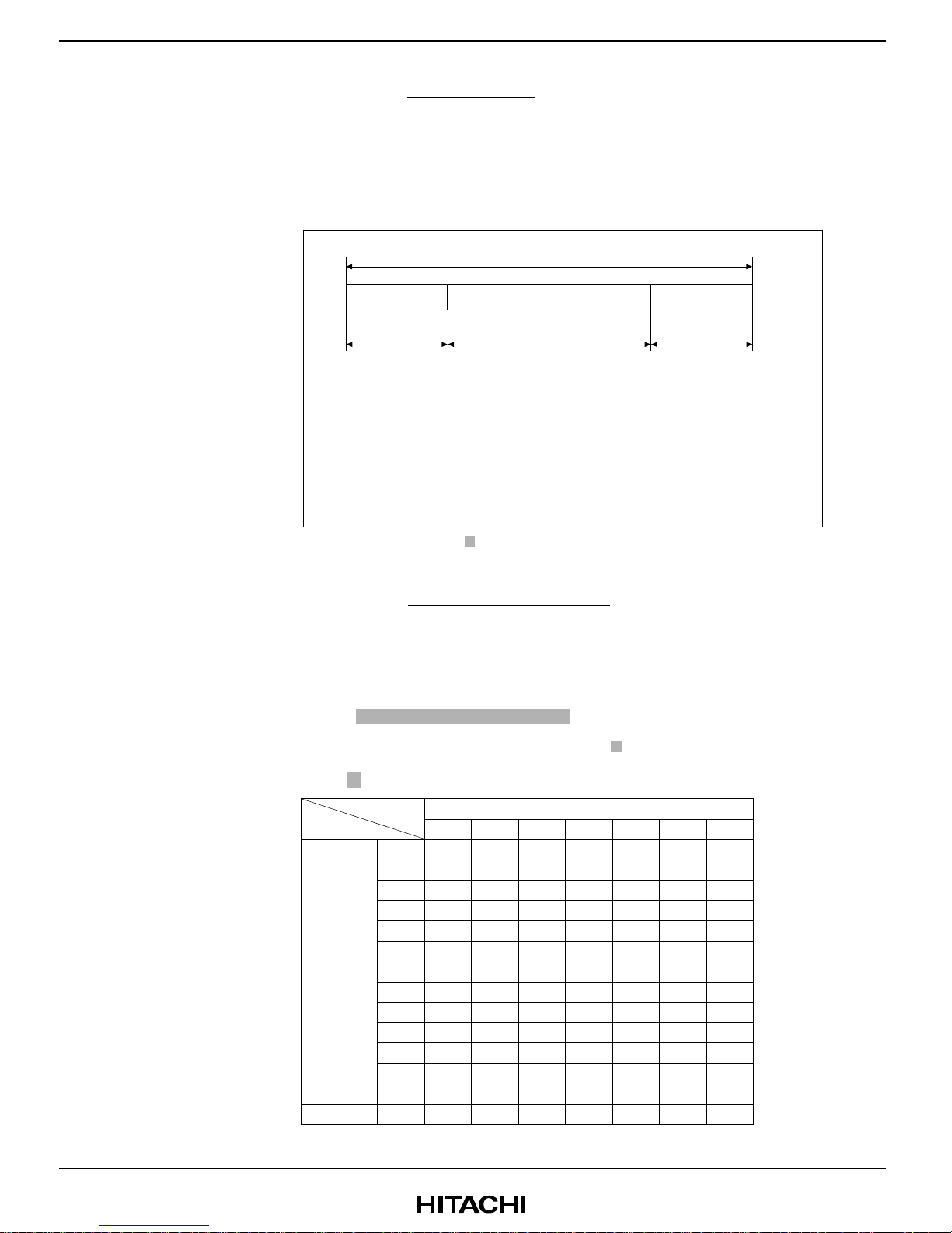
SYNC_SEG PRSEG PHSEG1 PHSEG2
1-bit time 1-bit time (8–25 time quanta)
Quantum
1 TSEG1 (time segment 1)
2–16
TSEG2 (time segment 2)
2–8
Legend
SYNC_SEG: Segment for establishing synchronization of nodes on the CAN bus. (Normal
bit edge transitions occur in this segment.)
PRSEG: Segment for compensating for physical delay between networks.
PHSEG1: uffer segment for correcting phase drift (positive). (This segment is extended
when synchronization (resynchronization) is established.)
PHSEG2: uffer segment for correcting phase drift (negative). (This segment is
shortened when synchronization (resynchronization) is established.)
Note: The time quanta values of TSEG1 and TSEG2 become the value of TSEG + 1.
Figure 15-6 Detailed Description of Timing within 1 it
HCAN bit rate calculation:
f
CLK
2 × ( RP + 1) × (3 + TSEG1 + TSEG2)
it rate =
Note: f
CLK
= ø (system clock)
The CR values are used for RP, TSEG1, and TSEG2.
CR Setting Constraints
TSEG1 > TSEG2 ≥ SJW (SJW = 0 to 3)
These constraints allow the setting range shown in table 15-4 for TSEG1 and TSEG2 in CR.
Table 15-4 Setting Range for TSEG1 and TSEG2 in CR
TSEG2 ( CR [14:12])
001 010 011 100 101 110 111
TSEG1 0011 No Yes No No No No No
( CR [11:8]) 0100 Yes*Yes Yes No No No No
0101 Yes*Yes Yes Yes No No No
0110 Yes*Yes Yes Yes Yes No No
0111 Yes*Yes Yes Yes Yes Yes No
1000 Yes*Yes Yes Yes Yes Yes Yes
1001 Yes*Yes Yes Yes Yes Yes Yes
1010 Yes*Yes Yes Yes Yes Yes Yes
1011 Yes*Yes Yes Yes Yes Yes Yes
1100 Yes*Yes Yes Yes Yes Yes Yes
1101 Yes*Yes Yes Yes Yes Yes Yes
1110 Yes*Yes Yes Yes Yes Yes Yes
1111 Yes*Yes Yes Yes Yes Yes Yes
Notes: The time quanta value for TSEG1 and TSEG2 is the TSEG value + 1.
*Only a value other than RP[13:8] = '000000 can be set.

Section Page Description
15.3.7 Interrupt 583 IRR3 Error warning interrupt (TEC ≥ 96)
Interface IRR4 Error warning interrupt (REC ≥ 96)
Table 15-5 HCAN
Interrupt Sources IRR7 Overload frame transmission interrupt
15.5 Usage Notes
9. HTxD pin output
in error passive state
10. Transition to
HCAN sleep mode
11. Message
transmission
cancellation (TxCR)
12. TxCR in the bus
off state
587 Newly added
9. HTxD pin output in error passive state
If the HRxD pin becomes fixed at 1 during message transmission or
reception when the HCAN is in the error active state, the HTxD pin will
output 0 continuously while in the error passive state. To stop continuous 0
output to the CAN bus, disable the HCAN by means of an error warning
interrupt or by setting the HCAN module stop mode through detection of a
fixed 1 state by the HxRD pin monitor.
10. Transition to HCAN sleep mode
The HCAN stops (transmission/reception stops) when MCR0 is cleared to 0
immediately after an HCAN sleep mode transition effected by setting TXPR
of the HCAN to 1 and setting MCR5 to 1. When a transition is made to the
HCAN sleep mode by means of the above steps, a 10-cycle wait should be
inserted after the TxPR setting. After an HCAN sleep mode transition,
release the HCAN sleep mode by clearing MCR5 to 0.
11. Message transmission cancellation (TxCR)
If all the following conditions are met when cancellation of a transmission
message is performed by means of TxCR of the HCAN, the TxCR or TxPR
bit indicating cancellation is not cleared even though internal transmission
is canceled.
When canceling a message using TxCR, 1 should be written continuously
until TxCR or TxPR becomes 0.
12. TxCR in the bus off state
If TxPR is set before the HCAN goes to the bus off state, and a transition is
made to the bus off state with transmission incomplete, cancellation will be
performed even if TxCR is set during the bus off period, and the message
will be transmitted after a transition to the error active state.
18.1.4 Register
Configuration
Table 18-2 LCD
Controller/Driver
Registers
633
LCD RAM —R/W Undefined H'FC40 to H'FC53
Module stop control
register D MSTPCRD R/W '11****** H'FC60
Note * 2 deleted
22.6.3 Setting
Oscillation
Stabilization Time
after Clearing
Software Standby
Mode
743 Note amended
Note: * Do not use this setting.

Section Page Description
23.1 Absolute
Maximum Ratings
Table 23-1
Absolute Maximum
Ratings
753
Input voltage (OSC1, OSC2) Vin –0.3 +3.5 V
lnput voltage (XTAL, EXTAL) Vin –0.3 to ACC +0.3 V
Input voltage (ports 4 and 9) Vin –0.3 to AVCC +0.3 V
Input voltage (ports A, , C, D, E,
ports PF2, PF4 to PF6) Vin –0.3 to LPVCC +0.3 V
Input voltage (ports H and J) Vin –0.3 to PWMVCC +0.3 V
Input voltage (except ports 4, 9, A,
, C, D, E, ports PF2, PF4 to PF6,
H and J)
Vin –0.3 to VCC +0.3 V
23.3 DC
Characteristics
Table 23-2 DC
Characteristics
755,
758
Input high
voltage RES, STBY,
NMI, FWE,
MD2 to MD0
V
IH
V
CC
– 0.7 —V
CC
+ 0.3 V
EXTAL V
CC
× 0.7 —V
CC
+ 0.3
Ports 1 to 3, 5,
H, J, K
Ports PF0, PF3,
PF7
2.2 —V
CC
+ 0.3
HRxD 2.2 —V
CC
+ 0.3
Ports A to E,
Ports PF2, PF4
to PF6
2.2 —LPV
CC
+ 0.3
Ports 4, 9 AV
CC
× 0.7 —AV
CC
+ 0.3
Input low
voltage RES, STBY,
NMI, FWE,
MD2 to MD0
V
IL
–0.3 —0.5 V
EXTAL –0.3 —0.8
Ports 1 to 3, 5,
A to F, H, J, K –0.3 —0.8
HRxD –0.3 —V
CC
+ 0.2
Notes amended
*1 If the A/D converter is not used, do not leave the AVCC, Vref , and AVSS pins
open. Apply a voltage between 4.5 V and 5.5 V to the AVCC and Vref pins by
connecting them to VCC, for instance. Set Vref ≤ AVCC.
*3 The values are for VRAM ≤ LPVCC < 3.0 V, VIH min = VCC × 0.9, and VIL max =
0.3 V.
23.4.1 Clock Timing
Table 23-4 Clock
Timing
761 (Incorrect)20MHz
(Correct)Condition
.1 Address 858 Data us Width of H'E C0 to H'EF F
(Incorrect)16/32
(Correct)8/16/32*

Section Page Description
.2 Functions 882 TXACK—Transmit Acknowledge Register H'F80A HCAN
15
TXACK7
0
R/(W)*
14
TXACK6
0
R/(W)*
13
TXACK5
0
R/(W)*
12
TXACK4
0
R/(W)*
11
TXACK3
0
R/(W)*
8
—
0
—
10
TXACK2
0
R/(W)*
9
TXACK1
0
R/(W)*
7
TXACK15
0
R/(W)*
6
TXACK14
0
R/(W)*
5
TXACK13
0
R/(W)*
4
TXACK12
0
R/(W)*
3
TXACK11
0
R/(W)*
0
TXACK8
0
R/(W)*
2
TXACK10
0
R/(W)*
1
TXACK9
0
R/(W)*
it
Initial value
Read/Write
it
Initial value
Read/Write
Note added
Note: * Only 1 can be written, to clear the flag.
883 A ACK—Abort Acknowledge Register H'F80C HCAN
15
A ACK7
0
R/(W)*
14
A ACK6
0
R/(W)*
13
A ACK5
0
R/(W)*
12
A ACK4
0
R/(W)*
11
A ACK3
0
R/(W)*
8
—
0
—
10
A ACK2
0
R/(W)*
9
A ACK1
0
R/(W)*
7
A ACK15
0
R/(W)*
6
A ACK14
0
R/(W)*
5
A ACK13
0
R/(W)*
4
A ACK12
0
R/(W)*
3
A ACK11
0
R/(W)*
0
A ACK8
0
R/(W)*
2
A ACK10
0
R/(W)*
1
A ACK9
0
R/(W)*
it
Initial value
Read/Write
it
Initial value
Read/Write
Note added
Note: * Only 1 can be written, to clear the flag.
RXPR—Receive Complete Register H'F80E HCAN
15
RXPR7
0
R/(W)*
14
RXPR6
0
R/(W)*
13
RXPR5
0
R/(W)*
12
RXPR4
0
R/(W)*
11
RXPR3
0
R/(W)*
8
RXPR0
0
R/(W)*
10
RXPR2
0
R/(W)*
9
RXPR1
0
R/(W)*
7
RXPR15
0
R/(W)*
6
RXPR14
0
R/(W)*
5
RXPR13
0
R/(W)*
4
RXPR12
0
R/(W)*
3
RXPR11
0
R/(W)*
0
RXPR8
0
R/(W)*
2
RXPR10
0
R/(W)*
1
RXPR9
0
R/(W)*
it
Initial value
Read/Write
it
Initial value
Read/Write
Note added
Note: * Only 1 can be written, to clear the flag.

Section Page Description
.2 Functions 884 RFPR—Remote Request Register H'F810 HCAN
15
RFPR7
0
R/(W)*
14
RFPR6
0
R/(W)*
13
RFPR5
0
R/(W)*
12
RFPR4
0
R/(W)*
11
RFPR3
0
R/(W)*
8
RFPR0
0
R/(W)*
10
RFPR2
0
R/(W)*
9
RFPR1
0
R/(W)*
7
RFPR15
0
R/(W)*
6
RFPR14
0
R/(W)*
5
RFPR13
0
R/(W)*
4
RFPR12
0
R/(W)*
3
RFPR11
0
R/(W)*
0
RFPR8
0
R/(W)*
2
RFPR10
0
R/(W)*
1
RFPR9
0
R/(W)*
it
Initial value
Read/Write
it
Initial value
Read/Write
Note added
Note: * Only 1 can be written, to clear the flag.
885,
886
IRR—Interrupt Register H'F812 HCAN
15
IRR7
0
R/(W)*
14
IRR6
0
R/(W)*
13
IRR5
0
R/(W)*
12
IRR4
0
R/(W)*
11
IRR3
0
R/(W)*
8
IRR0
1
R/(W)*
10
IRR2
0
R/(W)*
9
IRR1
0
R/(W)*
it
Initial value
Read/Write
0[Clearing condition]
Writing 1
1 Overload frame transmission
[Setting conditions]
When overload frame is transmitted
Overload Frame Interrupt Flag
7
—
0
—
6
—
0
—
5
—
0
—
4
IRR12
0
R/(W)*
3
—
0
—
0
IRR8
0
R/(W)*
2
—
0
—
1
IRR9
0
R/(W)*
it
Initial value
Read/Write
Note added
Note: * Only 1 can be written, to clear the flag.

Section Page Description
.2 Functions 890 UMSR—Unread Message Status Register H'F81A HCAN
15
UMSR7
0
R/(W)*
14
UMSR6
0
R/(W)*
13
UMSR5
0
R/(W)*
12
UMSR4
0
R/(W)*
11
UMSR3
0
R/(W)*
8
UMSR0
0
R/(W)*
10
UMSR2
0
R/(W)*
9
UMSR1
0
R/(W)*
7
UMSR15
0
R/(W)*
6
UMSR14
0
R/(W)*
5
UMSR13
0
R/(W)*
4
UMSR12
0
R/(W)*
3
UMSR11
0
R/(W)*
0
UMSR8
0
R/(W)*
2
UMSR10
0
R/(W)*
1
UMSR9
0
R/(W)*
it
Initial value
Read/Write
it
Initial value
Read/Write
Unread Message Status Flags
0 [Clearing condition]
Writing 1
(x = 15 to 0)
1 Unread receive message is overwritten by a new message
[Setting condition]
When a new message is received before RXPR is cleared
Note added
Note: * Only 1 can be written, to clear the flag.
1009 PFDR—Port F Data Register H'FF0E Port
7
—
0
R/W
6
PF6DR
0
R/W
5
PF5DR
0
R/W
4
PF4DR
0
R/W
3
PF3DR
0
R/W
0
PF0DR
0
R/W
2
PF2DR
0
R/W
1
—
Undefined
—
it
Initial value
Read/Write
C.12 Port F lock
Diagrams 1107
D
WDDRF
Reset
Internal data bus
R
Mode 4/5/6
S
C
QD
PF7DDR
*


i
Contents
Section 1 O er iew.......................................................................................... 1
1.1 O er iew............................................................................................................................ 1
1.2 Internal Block Diagram......................................................................................................6
1.3 Pin Description................................................................................................................... 8
1.3.1 Pin Arrangement................................................................................................... 8
1.3.2 Pin Functions in Each Operating Mode................................................................ 10
1.3.3 Pin Functions........................................................................................................ 20
Section 2 CPU.................................................................................................. 27
2.1 O er iew............................................................................................................................ 27
2.1.1 Features................................................................................................................. 27
2.1.2 Differences between H8S/2600 CPU and H8S/2000 CPU................................... 28
2.1.3 Differences from H8/300 CPU ............................................................................. 29
2.1.4 Differences from H8/300H CPU.......................................................................... 29
2.2 CPU Operating Modes....................................................................................................... 30
2.3 Address Space.................................................................................................................... 35
2.4 Register Configuration....................................................................................................... 36
2.4.1 O er iew............................................................................................................... 36
2.4.2 General Registers.................................................................................................. 37
2.4.3 Control Registers.................................................................................................. 38
2.4.4 Initial Register Values .......................................................................................... 40
2.5 Data Formats...................................................................................................................... 41
2.5.1 General Register Data Formats............................................................................. 41
2.5.2 Memory Data Formats.......................................................................................... 43
2.6 Instruction Set.................................................................................................................... 44
2.6.1 O er iew............................................................................................................... 44
2.6.2 Instructions and Addressing Modes...................................................................... 45
2.6.3 Table of Instructions Classified by Function........................................................ 47
2.6.4 Basic Instruction Formats..................................................................................... 56
2.7 Addressing Modes and Effecti e Address Calculation...................................................... 58
2.7.1 Addressing Mode.................................................................................................. 58
2.7.2 Effecti e Address Calculation.............................................................................. 61
2.8 Processing States................................................................................................................ 65
2.8.1 O er iew............................................................................................................... 65
2.8.2 Reset State ............................................................................................................ 66
2.8.3 Exception-Handling State..................................................................................... 67
2.8.4 Program Execution State ...................................................................................... 70
2.8.5 Bus-Released State................................................................................................ 70
2.8.6 Power-Down State................................................................................................ 70

ii
2.9 Basic Timing...................................................................................................................... 71
2.9.1 O er iew............................................................................................................... 71
2.9.2 On-Chip Memory (ROM, RAM).......................................................................... 71
2.9.3 On-Chip Supporting Module Access Timing....................................................... 73
2.9.4 On-Chip HCAN Module Access Timing.............................................................. 75
2.9.5 External Address Space Access Timing............................................................... 76
2.10 Usage Note......................................................................................................................... 76
2.10.1 TAS Instruction .................................................................................................... 76
2.10.2 Caution to obser e when using bit manipulation instructions.............................. 76
Section 3 MCU Operating Modes................................................................... 79
3.1 O er iew............................................................................................................................ 79
3.1.1 Operating Mode Selection.................................................................................... 79
3.1.2 Register Configuration.......................................................................................... 80
3.2 Register Descriptions......................................................................................................... 80
3.2.1 Mode Control Register (MDCR).......................................................................... 80
3.2.2 System Control Register (SYSCR)....................................................................... 81
3.2.3 Pin Function Control Register (PFCR)................................................................. 82
3.3 Operating Mode Descriptions............................................................................................ 84
3.3.1 Mode 4.................................................................................................................. 84
3.3.2 Mode 5.................................................................................................................. 84
3.3.3 Mode 6.................................................................................................................. 84
3.3.4 Mode 7.................................................................................................................. 84
3.4 Pin Functions in Each Operating Mode............................................................................. 85
3.5 Address Map in Each Operating Mode.............................................................................. 85
Section 4 Exception Handling......................................................................... 89
4.1 O er iew............................................................................................................................ 89
4.1.1 Exception Handling Types and Priority................................................................ 89
4.1.2 Exception Handling Operation ............................................................................. 90
4.1.3 Exception Vector Table........................................................................................ 90
4.2 Reset................................................................................................................................... 92
4.2.1 O er iew............................................................................................................... 92
4.2.2 Reset Sequence ..................................................................................................... 92
4.2.3 Interrupts after Reset............................................................................................. 94
4.2.4 State of On-Chip Supporting Modules after Reset Release.................................. 95
4.3 Traces................................................................................................................................. 95
4.4 Interrupts............................................................................................................................ 96
4.5 Trap Instruction.................................................................................................................. 97
4.6 Stack Status after Exception Handling .............................................................................. 98
4.7 Notes on Use of the Stack.................................................................................................. 99

iii
Section 5 Interrupt Controller..........................................................................101
5.1 O er iew............................................................................................................................ 101
5.1.1 Features................................................................................................................. 101
5.1.2 Block Diagram...................................................................................................... 102
5.1.3 Pin Configuration.................................................................................................. 103
5.1.4 Register Configuration.......................................................................................... 103
5.2 Register Descriptions......................................................................................................... 104
5.2.1 System Control Register (SYSCR)....................................................................... 104
5.2.2 Interrupt Priority Registers A to H, J, K, M
(IPRA to IPRH, IPRJ, IPRK, IPRM).................................................................... 105
5.2.3 IRQ Enable Register (IER)................................................................................... 106
5.2.4 IRQ Sense Control Registers H and L (ISCRH, ISCRL) ..................................... 107
5.2.5 IRQ Status Register (ISR) .................................................................................... 108
5.3 Interrupt Sources................................................................................................................ 109
5.3.1 External Interrupts................................................................................................ 109
5.3.2 Internal Interrupts ................................................................................................. 110
5.3.3 Interrupt Exception Handling Vector Table ......................................................... 110
5.4 Interrupt Operation............................................................................................................. 114
5.4.1 Interrupt Control Modes and Interrupt Operation ................................................ 114
5.4.2 Interrupt Control Mode 0...................................................................................... 117
5.4.3 Interrupt Control Mode 2...................................................................................... 119
5.4.4 Interrupt Exception Handling Sequence............................................................... 121
5.4.5 Interrupt Response Times..................................................................................... 122
5.5 Usage Notes ....................................................................................................................... 123
5.5.1 Contention between Interrupt Generation and Disabling ..................................... 123
5.5.2 Instructions that Disable Interrupts....................................................................... 124
5.5.3 Times when Interrupts are Disabled..................................................................... 124
5.5.4 Interrupts during Execution of EEPMOV Instruction.......................................... 125
5.5.5 IRQ Interrupts....................................................................................................... 125
5.6 DTC Acti ation by Interrupt.............................................................................................. 125
5.6.1 O er iew............................................................................................................... 125
5.6.2 Block Diagram...................................................................................................... 125
5.6.3 Operation .............................................................................................................. 126
Section 6 PC Break Controller (PBC)..............................................................129
6.1 O er iew............................................................................................................................ 129
6.1.1 Features................................................................................................................. 129
6.1.2 Block Diagram...................................................................................................... 130
6.1.3 Register Configuration.......................................................................................... 131
6.2 Register Descriptions......................................................................................................... 131
6.2.1 Break Address Register A (BARA)...................................................................... 131
6.2.2 Break Address Register B (BARB)...................................................................... 132

iv
6.2.3 Break Control Register A (BCRA)....................................................................... 132
6.2.4 Break Control Register B (BCRB) ....................................................................... 134
6.2.5 Module Stop Control Register C (MSTPCRC).................................................... 134
6.3 Operation............................................................................................................................ 135
6.3.1 PC Break Interrupt Due to Instruction Fetch........................................................ 135
6.3.2 PC Break Interrupt Due to Data Access ............................................................... 135
6.3.3 Notes on PC Break Interrupt Handling................................................................. 136
6.3.4 Operation in Transitions to Power-Down Modes................................................. 136
6.3.5 PC Break Operation in Continuous Data Transfer ............................................... 137
6.3.6 When Instruction Execution is Delayed by One State.......................................... 138
6.3.7 Additional Notes................................................................................................... 139
Section 7 Bus Controller..................................................................................141
7.1 O er iew............................................................................................................................ 141
7.1.1 Features................................................................................................................. 141
7.1.2 Block Diagram...................................................................................................... 142
7.1.3 Pin Configuration.................................................................................................. 143
7.1.4 Register Configuration.......................................................................................... 143
7.2 Register Descriptions......................................................................................................... 144
7.2.1 Bus Width Control Register (ABWCR) ............................................................... 144
7.2.2 Access State Control Register (ASTCR).............................................................. 144
7.2.3 Wait Control Registers H and L (WCRH, WCRL).............................................. 146
7.2.4 Bus Control Register H (BCRH).......................................................................... 150
7.2.5 Bus Control Register L (BCRL)........................................................................... 151
7.2.6 Pin Function Control Register (PFCR)................................................................. 152
7.3 O er iew of Bus Control................................................................................................... 154
7.3.1 Area Partitioning................................................................................................... 154
7.3.2 Bus Specifications ................................................................................................ 155
7.3.3 Memory Interfaces................................................................................................ 156
7.3.4 Interface Specifications for Each Area................................................................. 157
7.4 Basic Bus Interface............................................................................................................ 158
7.4.1 O er iew............................................................................................................... 158
7.4.2 Data Size and Data Alignment.............................................................................. 158
7.4.3 Valid Strobes ........................................................................................................ 160
7.4.4 Basic Timing......................................................................................................... 161
7.4.5 Wait Control.......................................................................................................... 169
7.5 Burst ROM Interface.......................................................................................................... 171
7.5.1 O er iew............................................................................................................... 171
7.5.2 Basic Timing......................................................................................................... 171
7.5.3 Wait Control.......................................................................................................... 173
7.6 Idle Cycle........................................................................................................................... 174
7.6.1 Operation .............................................................................................................. 174
7.6.2 Pin States During Idle Cycles............................................................................... 177
This manual suits for next models
5
Table of contents
Other Hitachi Desktop manuals

Hitachi
Hitachi HF-W2000 35 User manual

Hitachi
Hitachi CE50-10 User manual

Hitachi
Hitachi HF-BX1000 User manual

Hitachi
Hitachi 505 User manual

Hitachi
Hitachi MB-6890 User manual

Hitachi
Hitachi HF-W6500 User manual

Hitachi
Hitachi 65 User manual

Hitachi
Hitachi HF-W2000 35 User manual

Hitachi
Hitachi HF-W2000 User manual

Hitachi
Hitachi MB-6890 User manual
Popular Desktop manuals by other brands

Asus
Asus D700SE user guide

HP
HP Workstation xw3100 Quick setup

Intertec Data Systems
Intertec Data Systems SUPERBRAIN II Jr user manual

Dell
Dell Precision 3450 Small Form Factor Cable Cover install guide

HP
HP Envy Recline23 TouchSmart Beats SE... Disassembly instructions

BiGDUG
BiGDUG BiG400 Guide to Assembly & Usage