manuals.online logo
Brands
  1. Home
  2. •
  3. Brands
  4. •
  5. Hitachi
  6. •
  7. Desktop
  8. •
  9. Hitachi 505 User manual

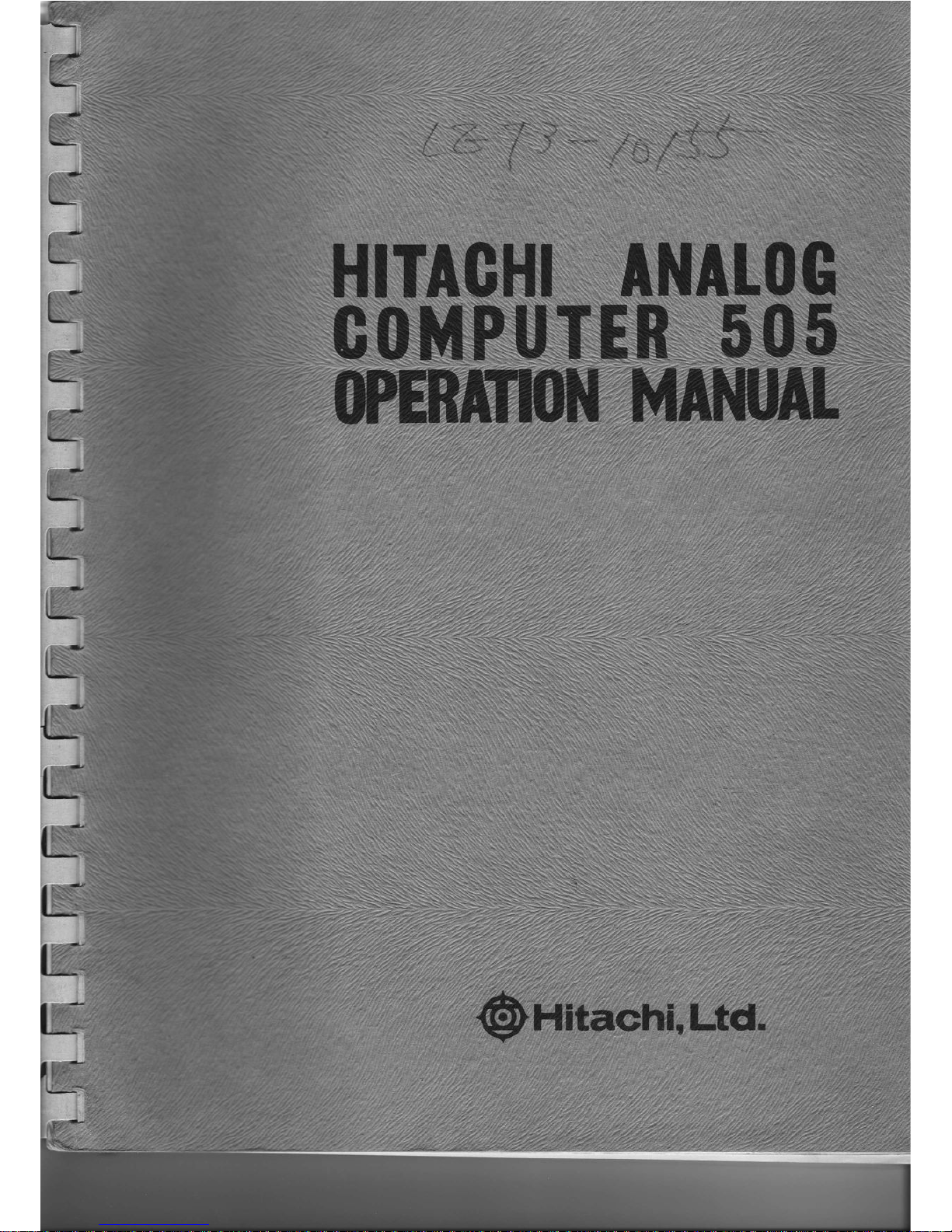
Hitachi 505 User manual

:
--
-
j-
-a:
--5
-l
-l
-l
-l
-1
-l
rJ
4't HITACHI ANALOG
COM?UTER
CO}ilIENIS
I - INTN,ODUCTION
II - THE
HITACHI 505 COMPIIIEH,
GENERAL
DESCRITTION
OF HIIACH]
?age
4
SECTION
SECTION
1.
2ö
t/
t/+
2T
21_
21,
u
/ö
217
)"7
3/+
lQ
l+2
l*7
OIER,AT
ING CONSIDERAT
IONS
a. ?relininary Operating Considerations
b. ?re-Patch Panel Insertion and Removal
c. Amplifier Balance
d. Changing Computational Components
MONII'ORTNG
AND
COIfIROL
a. Output Selector SL-25A """""'
b. Overload Indicator OL-25I
c. Digital Voltmeter DV-25L
d. Multi-Range Voltmeter (in the Contror Panel) "
e. Reference Potentiometer (in the Control
Panel)
f. Mode
Control (in ttre Control ?anel)
^ T nrnlrq
6.
h. Slave Switches
i. Readout Devices
(in the Control ?ane1) ........
j. Function
Switches '"""'''
k. ?ower
Switches (:n tne Qontrol Panel) """"
POTENTIOMETERS ""'' """.."""
o?EFATTONAI
AI4PT,TFTER'
........... "'"..""'
a. General
Considerations .."""..'
b. 505 Operational Araplifier DA-151 "" "
6. QUA.RfER.SQUAFB
MULTIPLIER
EM-151 56
a. MultiPlication 58
b. Division 62
7 . F'IJNCTION
CENERATORS
^ v2 pixed Function Generator FG-151r-A ........"
4. ^ r r^vq
ol+
ol
ol
67
na
öJ-
QC
AO
b. Log X Fixed Function
n Tni onnomctrie Fixed
r r rSvrrvrrrv er +v
d. Variable Function Ge
e. Variable F\rnction Ge
f: Varlable h:.nction Ge
Generator FG-155A
Functi-on Generator FG-153A
nerator FG-15I
nerat,or TG-j-52
nerator FG-L57 .aaaa.
8. OOMPAnATORS
cP-151, CP-I52
9. rlEE DToDES
FD-151 .. .
" '
10. TRANSIER
DELAY
ELE|'ENT
TD-151 " " " " '
11, AIJIOMATIC
OTERATOR
AO-151
T2. MODE
CONTROL
PANEL
MC-f51
LL. REFtrTIII\IE
OTERATION a02
...aaaat'""tttt"'
SECTTON
IlI - MA]NTENANCE' SB?ARATED
''HIIACHT ANA],OG
COMPUTER
TROGRAM
MANUA-L'I
Will EXPIA1N
thE PTOgTAMM1Ng
technique for HIIACHI 5A5
Computer.
The Manual is common
in programmi-ng
for all kinds of HIIACHI Analog
Conputer.
a.aaaa
11
€_
-
Fi.nr'm
Itrri,rber
all
afa
2 2-1
2.2-2
2.2-3
2.2-/+
2.2-5
1.1-O
aary
2.3-t
/ 1-/
2.3-3
2.3-/o
aJ'')
aJa
2.5-/+
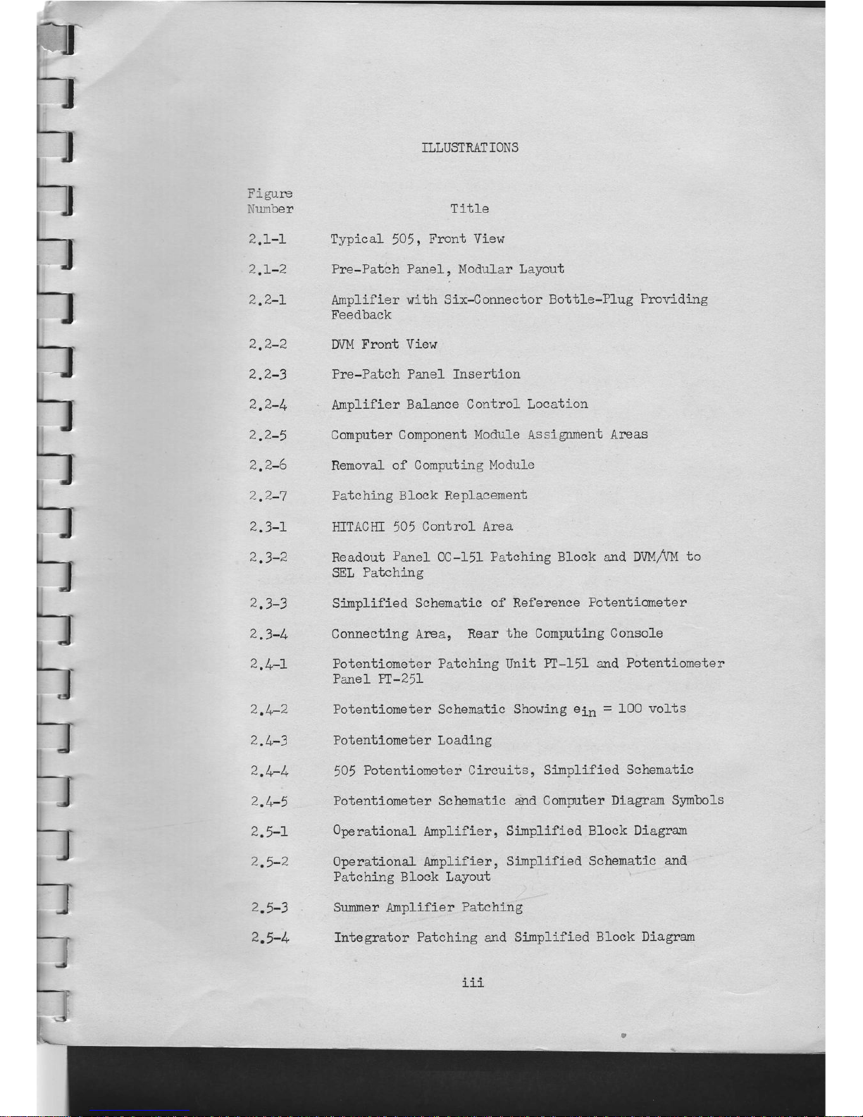
ILLUSTR.ATIONS
Title
Typical JOJ, Front Vlew
Pre-Patch Panel, Modular Layout
Amplifier with Six-Connector Bottle-?lug Providing
Feedback
DVMFront View
Pre-Patch Panel Insertion
Amplifier Balance Control Locatj-on
Computer Component
Module Assignment Areas
Removal of Conputing Module
Patching Block Replacement
HITACHI
505 Control Area
Readout Panel OC-151
Patching Block and DVMTA4
to
SEL
Patching
Qimnl ifiaä (nhamxtis Of Reference Potentiometer
Conneeting Ar€a, Rear the Comprting Console
Potentiometer Patching Unit PT-151 and ?otentiometer
Panel fr-Z5t
Potentiometer Schematic Showing
ein = 100 volts
Potentioneter Loading
6O4 Pntantinmotp- f'.i--rr.i*e crm-rified SchematiC
)vJ L v
Potenti-ometer Schematic ea'rd
Conputer Diagram Synbols
Operational tunplifier, Simplified Block Diagrarn
Operational Arnplifier, Simplified Schematic and
Patching Block Layout
SummerAmplifier Patching
Integrator Patching ard Simplified Block Diagrant
r_l_l_
/ n-l
z.o-)
z.o-2
4ry1
2.7-2
2.7-3
adl
2.7-5
z. /-o
<'. l-ö
2.7-9
1.l-LU
a.l-!4
2.7-U
2.7-1_5
2.8-L
2.10-1
T-+^-e-!^, n--- j l.i
er rha S,mnl i fi ed SchemrtiC
Irtu=SIauut ru.rlJ!rLfsf 4Lq ulrryrJJ!(
\rhht tl .te.] \ taer tlt.gram
r rut ulPrre
c^,,-*:- ^ ^i -^,,.1+ (innl i ni a^ snr.anatic
uYuarrrlS u, r!'rPrr
Mrr]tinlien Simnli].ia| R-lnnk llj2srnm r-i Dr*nhin''
1'1(! UIplfVt . Jlllplrr vLaA! a'l 411tr L , uu- tlIIE;
R-l nnlr T lrrnrrl.
M'rlt.inl icati on P^+^!.i-^ --Ä c'ih-] ified schenatic
lrurury*ru r auvrrrlr5 arrq ulrrPf-
ni--.r^j ^.^ D-+^r^j-., znd simn'l i -ied schemrtic
yf v!-furt r 4uurr!116
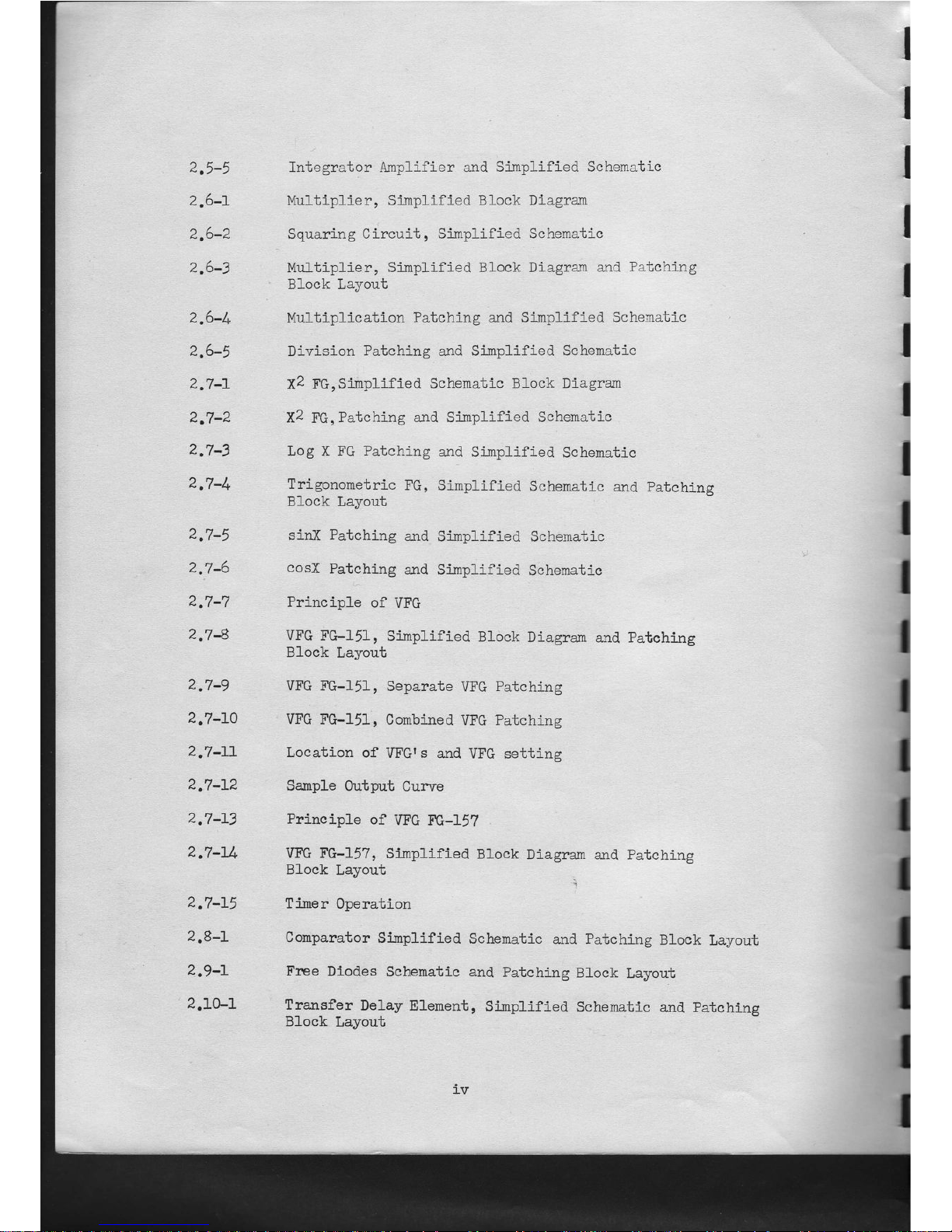
X2 FGrSimplified Schematic Block Diagran
X2 FG,
Patchlng arrd Simplified Schernatic
Log X FG Patching and Simplified Schematic
Trigonometric FG. Simplified Schematic and patching
IJVUÄ UAJVAU
sinX Patching and Simplified Schenatic
cosX Patching and Simplified Schematic
Pri nn i n'l o nf IIF|I
VFG
FG-151, Si-nplified Block Diagram and ?atching
H lnnr I a17^r1t
VFG FG-151, Separate VFG Patching
VFG FG-151, Combined VFG Patching
Location of VFGIs and VFG setting
Sample Output Curve
Principle of VFG TV-l-57
VFC FG-157, Sin,plified Bl-ock Diagram and Patching
H I ^nr | ä1r^11t
Timer Operation
Comparator Simplified Schematic and Patching Block Layout
Fr.ee
Diodes Schematic and ?atching Block T,ayout
Transfer Delay Elenent, Simplified Schematic and patching
Block Layout
I
I
I
I
I
I
I
I
I
I
I
I
I
I
I
I
I
I
I
l_v
L-,
I
q
!
l-t
It
h
hr
n
f-1,
f-{
f-r
f'-r
t'-t
n
f-l
fT
T
2.l-u-^z
2.f1-1
2.IL-2
2.I2-I
1.L)-L
1. LJ-1
!1an9fer Delay Element, Typical patching and
Simplified Schematic
Äutomatic Operator, Simplified Schematic and
Block Layout
Automatic Operator, Block Diagrarn
for Typical
Connection and patching nlocklayout
Mode
Control panel-
patching Block Layout
Timer Panel , TM-25I
Timer Operation
Patching
SECTION ]
IIüIRODUCTION
Many scientific problems studied today i-n various fields involve
the solution of parbial or ordinary differential equations. It is
the exception, rather than the ru1e, that the pr"oblerns adrnit' exact'
analybic solutions. The modern analog computero zuch as the Hltachi
505, provides a convenient nethod for obtaining numerical solutions
to zuch problems as well as enabling the scientist to study the effect
of changes ln the physical system.
The nethod of problem solution in an ,nalog computer is quite
sJmple. The conputer i-s used to ltbuildrr an electronic analogy which
obeys the same set of differential equations as the physical problem
to be studied. Once this nodel has been constructed, er;:eri-rnents may
1,.
\.^i'._1;.,...
! i
be performed on this nodel in lieu of experi.ments on the physical
system. Investigations which might be difficult to carry out on the
actual system becone quite feasible with this technique. For exa^np1e,
a ptrysician may wi-sh to study the effeet on blood presfllre in a cer-
tain portion of the brain in the event that a patient loses an ann.
It is irnlikely that this experiment would be perfonned by any mearls
other than simu].ationl
Since the analog computer rmodelsrr the problem' each problen
variable corresponds to, or is analogous,to, " computer voltage: A"
1..1.. f . ' ' '...,
these voltages are readily available for measurement, instrumenti-on
is enployed to measur€the problen variables as in an actual system.
Solutions may be continuously displayed on a readout oscilloscopet
perma^nently plotted on a strip chart or x-y plotter, or ni;merically
-1-
.|
evaluated by means
of a voftmeter or digital voltmeter'
The detailed steps necessary for problem solution will be dis-
cussed in detail in a later section' Briefly' one
must first con-
strrrctamathematicalmodelforthesystemtobestudied.oftensuch
a model is not avail-able. rn this case, there are anal0g computer
:.-
techniques available for generating a model fron äeta'taken from the
physicalsystem.Thenexbstepi-nvolvestheconstructionofacomputer
nblock diagram" (an array of summing
alnps, integrators' etc') r^rhich
obeys the same
differential equations as the systern
model' This dia-
gramisthenusedtoconnectcomputingelementsutilizingthepatchboard.
Sincethepatchboardmayberemovedfromthecomputerandanotherpatch.
board inserbed, it is not necessary to use computer time otherSthan for
actual comPutation.
Theproblemisnowreadyforcomputersolution..Aftermorrnting
the proper patchboard, the potentiorneters (u?otso) are set to corre-
spond to the physical problem constants ' The computer solution is now
obtained by pressing the rtcoMPUTElt
button. ?roblem variabfes may then
be observed and recorded as desired. Additional runs may
be rnade
with
differentphysicalconstants,problernvariables,initialconditions'
^+^
Thisnarrualdescribesthecomputeroperationandprograrrrmingin
detail.Itshouldbeemphasisedthataknor^lledgeofelectricalengi-
rieeringisnot'necessarytosuccessfullyoperateananalogcomputer'
Theblockdiagranapproachusedinthismanualiscommoni.nnanyfields..
Themanualdescrlbesthegeneralcomprrteroperatingcontrolsfirst.
Thisisfollowedbyamodulebyrnoduledescriptionofeacht'blackboxn,
-2-
I
I
r
r-l
t-.
I
i
l-
t
I
ll
including its input-output characteristics and photographs of actual
n.fnh]rnrrÄ annno^tinnq R:ein nroor:mmino i c ownl:ined in the nro-
y4vvttrt\JaLu uullltEu . uaJru *rrrlu
graJn
manual at an introductory level. The detailed example given in
bhis section may be used as a model for the userr s particul-ar problem
co*. rrn 'in *,ha mrnrrr'l +'i+'1 a^ tlAhn-l-inr*.innqll ovn] rinq tho enani:l
DVU 4P flMlE lll4llUaJt UaUJsq ö},PfrU4UrvllD , g^y!@frrp urlu pysvla!
features of the Hitachi 505 for more adva.ncedtechniques. It incfudes
function generation, transfer fr-mction simulation, md partial- dif-
ferential equation solution. Helpful suggestions for the use of the
automatic operation unit in optirnization problems and the Timer and
Logic Operations board in iterative methods is also included.
-3-
ri'110': ;T
j..j : '. : 5 -C:i T'.-rr"
1. GEIiEIilI DESCRITT]ÜIi
OT
HITAJ;{I !05
The Hitacb"i 5C5
1s a meclii-un
size rlesk-top generai purpose
analog computer having a wide variety of applications' This computer
maybeinstalledinanyofficeorlaboratorywithoutspecialconsidera-
tions as to power or temperature control' The power consumption is
quitelo.lu,easilyhandledbynorrnalofficewiring.Sincethiscomputer
supplies its or^m
internal operatlng en'rironment by means of an oven'
itdoesnotdependonanaccurat'eexternaltempera+'urecontrol'The
heatdeliveredtotheroombyther-rnititselfisaboutthes.ryneas
that delivered by a rnediutn
size laboratory oscilloscope '
The Hitac hL 5A5
is nodular in concept with solid stat'e components
used throughout)f. The modular arrangement of the computer permits
specialmachineconfigurationsdependingont.heuserlsrequirements.
The componen-[
arraJlgement
allows sirnplified wiring. color coding of
the modules aids in rapid identification of elements and simplifies
wiring checks.
The conpu-cer is housed in two cabinets ' the computer main frame
andthecontrolconsole.Theseunitsmaybeeasilyseparatedfor
transportation.Themaincomputerconsolecontainsthepatchboard
r^riththeassociatedcomputingcomponentsmountedinanovendirecti-y
behind the patchboard. Beneath the patch panel is a panel contai-ning
the anplifier overload inoicators, the readout addressing system' and
thecoefficientpotentiometerswiththeirassociatedindicatorlamps,
it ulith t,he excePtion
voltage rectifier
of the oscilloscoPe tube and a high
in if.
I
r
t
r
r
t
t
t
t
t
I
I
I
I
g
t
f-I
i
F
F
F
t
tr
lI
:I
-I
I
addressing buttons, and label plates. A control located immediately
to the teft of the patchboard operates the motor drive for removing
or replacing the patchboard. The lower panel of the main computing
consol-e is tilted toward the operator for ease of operation.
The power supply for the computing elements is located in thc
bottom rear of the cabinet. It is easily removed
for ser,rice or
transportation.
The control consol-e
contains the control panel, t'he oscillo-
scope, the iterative operation timer, the digital- logic rmit. and
the digital voltmeter. The control panel, located in the lower right
hand si,le of the control console, contains the manual rnode
control-
s"ritches, a --altmeter, the reference potentiometer, and Some
external
tnrü terminals. Immediately above this rmit is a three channel
oscilloscope with electronically generated scales. The digital volt-
meter mormted
above this oscilloscope may
be used for accurate
potenti-ometer setting and sofution readings. The iterative operation
timer, which may be used for sequential mode
control, is located in
the lower left corner of the control console. The digital logic unitt
mourrteddirectly above the timer module, contains various types of
I
patchable logic.
NOTES: 1. Ti{E DISPOSITION
CHANGED
SLIGHTLY
IN T}IE LATER
PRODUCTS.
2. ONEMOFE
COI,{PUTTNG
CONSOIE
}JIAY
M ADDED
TO TIm RIGHT OF
TI{E ABO]IE
COMPUTER.
FrGUm
2.L-L TYPTCAT
505, FRolflr
vEW
t
T
t
t
I
-A
;-E
l.tj
L:r
i
n
ft
H
fi
F
t
HA],F EQUTPPED
FIGUNS 2.L.2 PFE-PATCH
?ANELMODÜLARLAYOTIT
t-
FULLYEQUIPFED
2. OMRATING
CONSIDENATIONS
The HitachL 5O5
(F:-gure 2'1-1) is shipped complete with all
components in place except porrer supply and DVM' Each unit is com-
pletely cafibrated and adjusted at the time of manufacture ' After
perforrning the sirople installation and check procedure outfined in
the maintenance marulal
, md connecting the unit to a suitable polJer
sour€eo the computer is ready for operation'
The current hmiting circuits proi;ect the reference supplies
andallactiveoperationalelenentsfromdamageduetoshortingt.o
ground,ortoeachother.Thusanerrantpatchingcorr'nection(short-
ingtheplusreferencetogroundforexample)wi]-lnotadversely
effect the supplies (output current' drops to zero) nor will the re-
ference supply fuse blow. In addition, the surface of ?re-Patch Panel
is covered with coloured plastic plates (except' frarne and handles) re-
clucing shorting-out of ha-nging pat'eh cords.
a. ?reliminary Operating Considerations
The following sreps are recommended
prior to operating the Hitachi
505
to prevent possible false trouble indications.
(f) Ascertain that each operational amplifler has a six connector
bottle plug or a combination of bottl-e plugs equal to a six connector
bottlepluE:properlyplacedandseatedasshowninFigure2.2_I.
This provides the amplifiers r^rit,h
feedbaek artd prevent them from
overloading during the problem solution.
L*
t
r
r
(
c
c
4
=t
(b) srx-coIrr{EcTOR
BOTTLE-PLUG
FTGURE
2.2-L AMPLIFIER
I^IITHSIX CONNtrCTORBOTTLE-IT,UG
PROV]DT{G
FEqDBACK
r\
r,_r
h
rir
l-]
llr
Ilr DA-l51
-9-
DVMDV-251
(ttRAtto-votrtr swrrcH ADDEDrN LATER
ttoDEL)
DVM
ET 620
FTGURE2.2-N DVM
FROIfIVIEW
The procedure for inserti-ng and removing the pre-patch panel
is described in Paragraph
2.b.
(2) Patch the Digital vortmeter (nvru)
and multi-range voltmeter
(wt) to the selector readout system. (see Figure 2.J-2 and ?ara-
graph 2.c. of this section for a deseription of the selector system
nnonr*.i a- \
e) Apply power to the computer, then ?ot Set modewill appear.
rnitially the overload lamps of the operational arnplifiers r,rill_
light; after a few seconds all of the lamps should extinzuish.
(/r) check the vari-ous suppry voltages of the computer. All power
supply outputs are eonnected to the voltmeter switch in front of
the power supply through appropriate scaling resistors; the check
may be accomplished simply and rapidly.
(5) Check the plus and minus referenee
DVMby selecting 100 (red for plus) and
Paragraph 3.a.
(6) Allow about thirby minutes lrafln-up time; this assures that the
computing components, (including the DVI'{and oscilloscope) are up
to normal- operating temperature. Ground the DW input ter:nination
(designated on the oc-151 FEADOIIT
?AliET,), md confinn the reading is
within 000.00 plus or minus one bit. other adjustment for DVM
will
be necessary according to Model of DVM,
for DV-251, the zero check
is the only step necessary to assure thl correct operation.
(7) rn the Por SEf mode of the cornputer (pon sET button on the con-
trol pane1, model CT-25I depressed), closed relay contacts prov:ide a
feedback cj-rcuit for the operational amplifier. (see paragraph { of
this section for a more detailed description)
supplied for readout on the
1OO
(blue for rninus). See
-11 -
This feature perrnits the removal of the ?re-Patch ?anel
to balance the operational amplifier' However' when
the com-
puter is switched from POT
SET to any other mod'e
' the relay
contact's open and the circuits as patched on the Pre-Patch
Parre}providesthefeedbackloop.Mornentaryamplifieroverload.
nay rezult during the relay operating time; thus to eHminate
possibleerrorinthecomputersolutlon,theoperatorshouJd
always sr^ritch the conputer FESET
(depress the FESET
button) or
Al,l, FESET
(depress Al,t FESI butt'on for nulti-mod'e operation
only), before switching to the COMPIJIE
or REP
O?
nrode' This
pennit the pot set relays to open and the implifier suruning
junctions to settle before starting the problem solution'
There is no actural rraiting period required; that is' tb
operator may depress the FESET
or AJ'L
RESEa
button and then
inrnediately depress the button for the desired mode' This
sequence of operation will prevent the possible momentary over-
load from effecting the problem solution'
b. ?re-?atch Panel Insertion and Removal
Tojnsertthe?re-Patch?anel'sett'helipont'helor^reredgeofthe
panel in the quide groove (f:-gure 2'2-3)' Push the top of the panel in
so the panel is verbical until the panel is clarnped autoroatically'
DepresstheENG(foTENGAGE)trrttononthelowerleftedgeofthe
cornputingconso].e.Thisbuttonproperlys"'täandfirnlyholdst,hePre-
?atch ?anel in position. As the ENG
and Drs (for DrSENGAGE)
br:ttons can
memorizetheoperatoraetion,itisnotnecessarytokeepthebuttonde-
pressedrrntilthepanelisloaded.IntheENGstate,aftertheparrelis
loaded,theparrelcannotberemovedrrnlesstheDlsbuttonispushed.
\
I
I
I
I
I
I
t-,
l''-t
th
FIGURE
2,2-3 PFE-PATCH
PANEL
TNSERTTON
_L3
-
ln the ENG
state without the panel, the panel can not be loaded. This
feature elimj.nates the possibility of accidentally engaging or dis-
engaging the Pre-Patch Panel.
The removal of the Pre-?atch panel is essentially the opposite of
inserbing the panel. Depress the Drs button, and depress the levers
on both handle of the panel. Then pult the panel towards the operator
upper edge of the panel first.
rt is not necessary to keep the panel straight by hand after in-
serbing the panel or after pushing the DIS button.
c. Anplifier Balance
The d-c operational anplifiers are chopper stabilized to prevent
drift and resultant errors in the conputer results. Drift in an am-
plifi-er results in an output voltage (or offset) with a zero inp-rt.
To elininate offset, the arnplifiers of the 505 are balanced, i.e., with
a bias current is applied to the amplifier summing
j'nction equal and
opposite to any current due to drift thus placing the surnnring
junction
at virtual gror:nd. Once balanced, drift in the amplifiers is el-iminated
automatically by the stabilizer circuit.
The d-c emplifj-ers of the 505 are ertremely stable and nornally do
not require balancing for periods up to several months. To assure ac-
curacy and confidence in the computer results, it may be desirable to
check the amplifier balance daily; this check can be made rapidly and
simply since the selector system and voltmeter are used.
There are two types of an,plifier balance in the JoJ; the voltage
balance check and current balance check. usual1y, only voltage balance
cheek will be sufficient for each amplifier. The current balance check
j-s necessary to reduce integrator drift, but the operator need not check
t
I
t
t
t
t
t
(
I
:
,o
:
./
:
L
tI
tl
t
t
t
- 1/, -

Other Hitachi Desktop manuals

Hitachi HF-W6500 User manual

Hitachi

Hitachi HF-W6500 User manual

Hitachi CE50-10 User manual

Hitachi

Hitachi CE50-10 User manual

Hitachi MB-6890 User manual

Hitachi

Hitachi MB-6890 User manual

Hitachi H8S/2646 User manual

Hitachi

Hitachi H8S/2646 User manual

Hitachi HF-W2000 35 User manual

Hitachi

Hitachi HF-W2000 35 User manual

Hitachi 65 User manual

Hitachi

Hitachi 65 User manual

Hitachi HF-W2000 User manual

Hitachi

Hitachi HF-W2000 User manual

Hitachi HF-W2000 35 User manual

Hitachi

Hitachi HF-W2000 35 User manual

Hitachi MB-6890 User manual

Hitachi

Hitachi MB-6890 User manual

Hitachi HF-BX1000 User manual

Hitachi

Hitachi HF-BX1000 User manual

Popular Desktop manuals by other brands

Sony PCV-RX680G - Vaio Desktop Computer Specifications

Sony

Sony PCV-RX680G - Vaio Desktop Computer Specifications

IEI Technology ECK-1000 Series user manual

IEI Technology

IEI Technology ECK-1000 Series user manual

Dell Vostro 260 Setup and features information

Dell

Dell Vostro 260 Setup and features information

IBM NetVista A21 Quick reference guide

IBM

IBM NetVista A21 Quick reference guide

HP dx2100 - Microtower PC Service & reference guide

HP

HP dx2100 - Microtower PC Service & reference guide

HP Slim 290 Disassembly instructions

HP

HP Slim 290 Disassembly instructions

Spirit P8Q67-M-DO user guide

Spirit

Spirit P8Q67-M-DO user guide

Dell EMC PowerEdge XR11 Installation and service manual

Dell

Dell EMC PowerEdge XR11 Installation and service manual

Lenovo ThinkStation S20 Uživatelská příručka

Lenovo

Lenovo ThinkStation S20 Uživatelská příručka

Asus Vintage-S800 quick start guide

Asus

Asus Vintage-S800 quick start guide

Zotac ZBOX series quick start guide

Zotac

Zotac ZBOX series quick start guide

Lenovo ThinkStation D30 Hardware Maintenance Manual

Lenovo

Lenovo ThinkStation D30 Hardware Maintenance Manual

EMAC IBX-200-VX800 Quick installation guide

EMAC

EMAC IBX-200-VX800 Quick installation guide

Lenovo ThinkCentre M51 Benutzerhandbuch

Lenovo

Lenovo ThinkCentre M51 Benutzerhandbuch

Panasonic Toughbook CF-18 Series Reference manual

Panasonic

Panasonic Toughbook CF-18 Series Reference manual

Avigilon NVR4X user guide

Avigilon

Avigilon NVR4X user guide

Panasonic CF-37 Series Reference manual

Panasonic

Panasonic CF-37 Series Reference manual

HP Z4 G4 Maintenance and service guide

HP

HP Z4 G4 Maintenance and service guide

manuals.online logo
manuals.online logoBrands
  • About & Mission
  • Contact us
  • Privacy Policy
  • Terms and Conditions

Copyright 2025 Manuals.Online. All Rights Reserved.