Holtek HT82B60R User manual

HT82B60R
I/O MCU with USB Interface
Rev. 1.10 1 February 1, 2011
General Description
The HT82B60R is a high performance, RISC architec-
ture microcontroller device specifically designed for
multiple I/O control product applications.
The advantages of low power consumption, I/O flexibil-
ity, timer functions, integrated USB interface, serial in-
terfaces, LCD drive capability, power down and
wake-up functions, watchdog timer etc, make the de-
vice extremely suitable for use in computer peripheral
product applications as well as many other applications
such as industrial control, consumer products, subsys-
tem controllers, etc.
These wide range of functions, together with a fully inte-
grated 6MHz or 12MHz oscillator, ensure that products
can be implemented with a minimum of external compo-
nents and smaller circuit board areas, providing users
with the benefits of lower overall product costs.
Features
·Operating voltage:
fSYS=6M/12MHz: 3.3V~5.5V
·Low voltage reset function
·42 bidirectional I/O lines (max.)
·8-bit programmable timer/event counter with
overflow interrupt
·16-bit programmable timer/event counter and
overflow interrupts
·Watchdog Timer
·PS2 and USB modes supported
·USB 2.0 low speed function
·4 endpoints supported -- endpoint 0 included
·8192´16 program memory
·216´8 data memory RAM
·Integrated 1.5kWresistor between V33O and
USBPDN pins for USB applications
·Fully integrated 6MHz or 12MHz oscillator
·All I/O pins have wake-up functions
·Power-down function and wake-up feature reduce
power consumption
·Serial Interface Module -- I2C and SPI functions
·4 COM lines for LCD display driving
·External interrupt pin
·8-level subroutine nesting
·Up to 0.33ms instruction cycle with 12MHz system
clock at VDD=5V
·Bit manipulation instruction
·15-bit table read instruction
·63 powerful instructions
·All instructions in one or two machine cycles
·20/28/48-pin SSOP, 32-pin QFN and
48-pin LQFP packages

Block Diagram
Pin Assignment
HT82B60R
Rev. 1.10 2 February 1, 2011
D a t a
M e m o r y
I/O
P o r t s
8 - b i t
T i m e r
W a t c h d o g
T i m e r
O T P P r o g r a m
M e m o r y
8 - b i t
R I S C
M C U
C o r e
W a t c h d o g
T i m e r O s c i l l a t o r
R e s e t
C i r c i t
I n t e r r p t
C o n t r o l l e r
6 / 1 2 M H z
I n t e r n a l O s c i l l a t o r
Low
V o l t a g e
R e s e t
P r o g r a m m a b l e
F r e q e n c y
G e n e r a t o r
U S B
V 3 3 O
L C D
D r i v e r
1 6 - b i t
T i m e r
I C / S P I
I n t e r f a c e
2
2 0
1 9
1 8
1 7
1 6
1 5
1 4
1 3
1 2
1 1
1
2
3
4
5
6
7
8
9
1 0
H T 8 2 B 6 0 R
2 0 S S O P - A
P B 6
P B 7
V D D
V 3 3 O
U S B P D N / D A T A
U S B P D P / C L K
P E 0
P E 1
G N D
R E S
P B 1
P B 0
P A 7 / T M R 1
P A 6 / T M R 0
P A 5
P A 4
P A 3
P A 2
P A 1
P A 0
1
2
3
4
5
6
7
8
9 1 0 1 1 1 2 1 3 1 4 1 5 1 6
1 7
1 8
1 9
2 0
2 1
2 2
2 3
2 4
2 52 62 72 82 93 03 13 2
P B 0 / S D I / S D A
P B 1 / S D O
P B 2 / S C K / S C L
P B 3 / S C S
P B 4 / P C K
P B 5 / E X T
P B 6
P B 7
H T 8 2 B 6 0 R
3 2 Q F N - A
R E S
G N D
P E 1
P E 0
U S B P D P / C L K
U S B P D N / D A T A
V 3 3 O
V D D
P C 7
P C 6
P C 5
P C 4
P C 3
P C 2
P C 1
P C 0
P A 0
P A 1
P A 2
P A 3
P A 4
P A 5
P A 6 / T M R 0
P A 7 / T M R 1
2 8
2 7
2 6
2 5
2 4
2 3
2 2
2 1
2 0
1 9
1 8
1 7
1 6
1 5
1
2
3
4
5
6
7
8
9
1 0
1 1
1 2
1 3
1 4
P B 3 / S C S
P B 2 / S C K / S C L
P B 1 / S D O
P B 0 / S D I / S D A
P A 7 / T M R 1
P A 6 / T M R 0
P A 5
P A 4
P A 3
P A 2
P A 1
P A 0
P C 7
P C 6
P B 4 / P C K
P B 5 / E X T
P B 6
P B 7
V D D
V 3 3 O
U S B P D N / D A T A
U S B P D P / C L K
P E 0
P E 1
G N D
R E S
P C 0
P C 1
H T 8 2 B 6 0 R
2 8 S S O P - A
4 8
4 7
4 6
4 5
4 4
4 3
4 2
4 1
4 0
3 9
3 8
3 7
3 6
3 5
3 4
3 3
3 2
3 1
3 0
2 9
2 8
2 7
2 6
2 5
1
2
3
4
5
6
7
8
9
1 0
1 1
1 2
1 3
1 4
1 5
1 6
1 7
1 8
1 9
2 0
2 1
2 2
2 3
2 4
H T 8 2 B 6 0 R
4 8 S S O P - A
P E 2
P E 3
P E 4
P E 5
P E 6
P E 7
P F 0
P F 1
V D D
V 3 3 O
U S B P D N / D A T A
U S B P D P / C L K
P E 0
P E 1
G N D
R E S
P C 0 / C O M 0
P C 1 / C O M 1
P C 2 / C O M 2
P C 3 / C O M 3
P D 0
P D 1
P D 2
P D 3
P B 7
P B 6
P B 5
P B 4
P B 3 / S C S
P B 2 / S C K / S C L
P B 1 / S D O
P B 0 / S D I / S D A
P A 7 / T M R 1
P A 6 / T M R 0
P A 5
P A 4
P A 3
P A 2
P A 1
P A 0
P C 7
P C 6
P C 5
P C 4
P D 7
P D 6
P D 5
P D 4
13 14 15 16 17 18 19 20 21 22 23 24
48 47 46 45 44 43 42 41 40 39 38 37
1
2
3
4
5
6
7
8
9
1 0
1 1
1 2
3 6
3 5
3 4
3 3
3 2
3 1
3 0
2 9
2 8
2 7
2 6
2 5
H T 8 2 B 6 0 R / H T 8 2 B 6 0 A
4 8 L Q F P - A
P E 2
P E 3
P E 4
P E 5
P E 6
P E 7
P F 0
P F 1
V D D
V 3 3 O
U S B P D N / D A T A
U S B P D P / C L K
P A 3
P A 2
P A 1
P A 0
P C 7
P C 6
P C 5
P C 4
P D 7
P D 6
P D 5
P D 4
P A 4
P A 5
P A 6 / T M R 0
P A 7 / T M R 1
P B 0 / S D I / S D A
P B 1 / S D O
P B 2 / S C K / S C L
P B 3 / S C S
P B 4
P B 5
P B 6
P B 7
P D 3
P D 2
P D 1
P D 0
P C 3 / C O M 3
P C 2 / C O M 2
P C 1 / C O M 1
P C 0 / C O M 0
R E S
G N D
P E 1
P E 0

Pin Description
Pin Name I/O Options Description
PA0~PA5
PA6/TMR0
PA7/TMR1
I/O
Pull-high
Wake-up
NMOS/CMOS/PMOS
Bidirectional 8-bit input/output port. Each pin can be configured as
a wake-up input by a configuration option. Software instructions de-
termine if the pin is a CMOS output or NMOS, PMOS or Schmitt
Trigger input. Configuration options determine if the structures are
CMOS, NMOS or PMOS types. Configuration options determine if
the pins have pull-high resistors. TMR0 and TMR1 are pin-shared
with PA6 and PA7, respectively.
PB0/SDI/SDA
PB1/SDO
PB2/SCK/SCL
PB3/SCS
PB4/PCK
PB5/INT
PB6~PB7
I/O Pull-high
Wake-up
Bidirectional 8-bit input/output port. Each nibble can be configured
as a wake-up input by a configuration option. Software instructions
determine if the pin is a CMOS output or Schmitt Trigger input. Con-
figuration options determine if the pins have pull-high resistors. The
power supply for I/O pins PB0~PB7 can be selected to be VDD or
V33O using a configuration option. Pins PB0~PB3 are pin-shared
with the Serial Interface pins. Pin PB4 is pin-shared with the periph-
eral clock output and PB5 is shared with the external interrupt pin.
PC0/COM0
PC1/COM1
PC2/COM2
PC3/COM3
PC4~PC7
I/O Pull-high
Wake-up
Bidirectional 8-bit input/output port. Each nibble can be configured
as a wake-up input by a configuration option. Software instructions
determine if the pin is a CMOS output or Schmitt Trigger input. Con-
figuration options determine if the pins have pull-high resistors.
PC0~PC3 are pin-shared with COM0~COM3
PD0~PD7 I/O Pull-high
Wake-up
Bi-directional 8-bit input/output port. Each nibble can be configured
as a wake-up input by a configuration option. Software instructions
determine if the pin is a CMOS output or Schmitt Trigger input. Con-
figuration options determine if the pins have pull-high resistors.
PE0~PE7 I/O Pull-high
Wake-up
Bidirectional 8-bit input/output port. Each nibble can be configured
as a wake-up input by a configuration option. Software instructions
determine if the pin is a CMOS output or Schmitt Trigger input. Con-
figuration options determine if the pins have pull-high resistors.
PF0, PF1 I/O Pull-high
Wake-up
Bidirectional 2-bit input/output port. Each pin can be configured as
a wake-up input by a configuration option. Software instructions de-
termine if the pin is a CMOS output or Schmitt Trigger input. Config-
uration options determine if the pins have pull-high resistors.
USBPDP/CLK I/O ¾USBPDP line. USB function is controlled by software control regis-
ters.
USBPDN/DATA I/O ¾USBPDN line. USB function is controlled by software control regis-
ters.
RES I¾Schmitt trigger reset input. Active low
GND ¾¾
Digital negative power supply, ground
VDD ¾¾
Digital positive power supply
V33O O ¾3.3V regulator output
Note: As the Pin Description table applies to the largest package size not all pin may exist on smaller packages.
Absolute Maximum Ratings
Supply Voltage ...........................VSS-0.3V to VSS+6.0V Storage Temperature ............................-50°Cto125°C
Input Voltage..............................VSS-0.3V to VDD+0.3V Operating Temperature...........................-40°Cto85°C
IOL Total ..............................................................150mA IOH Total............................................................-100mA
Total Power Dissipation .....................................500mW
Note: These are stress ratings only. Stresses exceeding the range specified under ²Absolute Maximum Ratings²may
cause substantial damage to the device. Functional operation of this device at other conditions beyond those listed
in the specification is not implied and prolonged exposure to extreme conditions may affect device reliability.
HT82B60R
Rev. 1.10 3 February 1, 2011

D.C. Characteristics Ta=25°C
Symbol Parameter
Test Conditions
Min. Typ. Max. Unit
VDD Conditions
VDD
Operating Voltage
(Integrated Oscillator) ¾fSYS=6MHz or 12MHz 3.3 ¾5.5 V
IDD Operating Current 5V
No load, fSYS=6MHz ¾6.5 12 mA
No load, fSYS=12MHz ¾7.5 16 mA
ISTB1 Standby Current 5V
No load, system HALT,
USB mode,
USR.5=1 USR.4=0,
LVR disable, WDT disable,
Clr D_SR [SCC.2],
Clr USBCKEN [SCC.3],
Clr BGOFF [SCC.4],
Set CLK_adj [SCC.7]
¾¾
400 mA
ISTB2 Standby Current 5V
No load, system HALT,
PS2 mode,
USR.5=0 USR.4=1,
LVR disable, WDT disable,
Clr D_SR [SCC.2],
Clr USBCKEN [SCC.3],
Set BGOFF [SCC.4],
Set CLK_adj [SCC.7]
¾¾10 mA
VIL
Input Low Voltage for PA, PC, PD,
PE, PF0~PF1
5V where VDDIO=VDD
or V33O by option for PB
0¾0.8 V
Input Low Voltage for PB 0 ¾0.3VDDIO V
Input Low Voltage for RES pin 0 ¾0.4VDD V
VIH
Input High Voltage for PA, PC, PD,
PE, PF0~PF1
5V where VDDIO=VDD
or V33O by option for PB
2¾5V
Input High Voltage for PB 0.8VDDIO ¾VDDIO V
Input High Voltage for RES pin 0.9VDD ¾VDD V
VLVR Low Voltage Reset 5V ¾2.0 2.6 3.2 V
VV33O
3.3V Regulator Output for
USB SIE 5V IV33O=70mA 3.0 3.3 3.6 V
IOL Output Sink Current for I/O Port 5V VOL=0.4V 24¾mA
IOH Output Source Current for I/O Port 5V VOH=3.4V -2-4¾mA
ILCD_BIAS VDD/2 Bias current for LCD 5V
LCDC. RSEL[1:0]=00 17.5 25 32.5 mA
LCDC. RSEL[1:0]=01 35 50 65 mA
LCDC. RSEL[1:0]=10 70 100 130 mA
LCDC. RSEL[1:0]=11 140 200 260 mA
VCOM VDD/2 voltage for LCD COM port 5V No load 0.475 0.500 0.525 VDD
RPH
Pull-high Resistance for CLK,
DATA
5V ¾
¾4.7 ¾kW
Pull-high Resistance for PA, PB,
PC, PD, PE and PF0~PF1 20 50 70 kW
HT82B60R
Rev. 1.10 4 February 1, 2011

A.C. Characteristics Ta=25°C
Symbol Parameter
Test Conditions
Min. Typ. Max. Unit
VDD Conditions
fRCSYS RC Clock with 8-bit Prescaler Register 5V ¾14 32 48 kHz
tWDT
Watchdog Time-out Period
(System Clock) ¾¾
1024 ¾¾
1/fRCSYS
tUSB USBPDP, USBPDN Rising & Falling Time ¾¾ 75 ¾300 ns
tOST Oscillation Start-up Timer Period ¾¾ ¾
1024 ¾tSYS
tOSCsetup Crystal Setup ¾¾ ¾
5¾ms
fINO125V Internal Oscillator Frequency for 12MHz 4.0V~
5.5V ¾10.80 12.00 13.20 MHz
fINO123V Internal Oscillator Frequency for 12MHz 3.0~
4.0V ¾10.56 12.00 13.44 MHz
fINOUSB
Internal Oscillator Frequency with USB
Mode
4.2~
5.5V ¾11.82 12.00 12.18 MHz
Note: tSYS=1/fSYS
Power_on period = tWDT +t
OST +t
OSCsetup
WDT Time_out in Normal Mode = 1/ fRCSYS ´256 ´WDTS + tWDT
WDT Time_out in Power Down Mode = 1/ fRCSYS ´256 ´WDTS + tOST +t
OSCsetup
Trimmed for 5V operation using factory trim values. Frequency Trim to 12MHz ±3%
HT82B60R
Rev. 1.10 5 February 1, 2011

HT82B60R
Rev. 1.10 6 February 1, 2011
System Architecture
A key factor in the high-performance features of the
Holtek range of microcontrollers is attributed to the inter-
nal system architecture. The range of devices take ad-
vantage of the usual features found within RISC
microcontrollers providing increased speed of operation
and enhanced performance. The pipelining scheme is
implemented in such a way that instruction fetching and
instruction execution are overlapped, hence instructions
are effectively executed in one cycle, with the exception
of branch or call instructions. An 8-bit wide ALU is used
in practically all operations of the instruction set. It car-
ries out arithmetic operations, logic operations, rotation,
increment, decrement, branch decisions, etc. The inter-
nal data path is simplified by moving data through the
Accumulator and the ALU. Certain internal registers are
implemented in the Data Memory and can be directly or
indirectly addressed. The simple addressing methods of
these registers along with additional architectural fea-
tures ensure that a minimum of external components is
required to provide a functional I/O and A/D control sys-
tem with maximum reliability and flexibility.
Clocking and Pipelining
The system clock is derived from an internal oscillator
and is subdivided into four internally generated
non-overlapping clocks, T1~T4. The Program Counter
is incremented at the beginning of the T1 clock during
which time a new instruction is fetched. The remaining
T2~T4 clocks carry out the decoding and execution
functions. In this way, one T1~T4 clock cycle forms one
instruction cycle. Although the fetching and execution of
instructions takes place in consecutive instruction cy-
cles, the pipelining structure of the microcontroller en-
sures that instructions are effectively executed in one
instruction cycle. The exception to this are instructions
where the contents of the Program Counter are
changed, such as subroutine calls or jumps, in which
case the instruction will take one more instruction cycle
to execute.
For instructions involving branches, such as jump or call
instructions, two machine cycles are required to com-
plete instruction execution. An extra cycle is required as
the program takes one cycle to first obtain the actual
jump or call address and then another cycle to actually
execute the branch. The requirement for this extra cycle
should be taken into account by programmers in timing
sensitive applications.
Program Counter
During program execution, the Program Counter is used
to keep track of the address of the next instruction to be
executed. It is automatically incremented by one each
time an instruction is executed except for instructions,
such as ²JMP²or ²CALL²that demand a jump to a
non-consecutive Program Memory address. It must be
noted that only the lower 8 bits, known as the Program
Counter Low Register, are directly addressable by user.
F e t c h I n s t . ( P C )
E x e c t e I n s t . ( P C - 1 ) F e t c h I n s t . ( P C + 1 )
E x e c t e I n s t . ( P C ) F e t c h I n s t . ( P C + 2 )
E x e c t e I n s t . ( P C + 1 )
P C P C + 1 P C + 2
O s c i l l a t o r C l o c k
( S y s t e m C l o c k )
P h a s e C l o c k T 1
P r o g r a m C o n t e r
P h a s e C l o c k T 2
P h a s e C l o c k T 3
P h a s e C l o c k T 4
P i p e l i n i n g
System Clocking and Pipelining
F e t c h I n s t . 1 E x e c t e I n s t . 1
F e t c h I n s t . 2
F l s h P i p e l i n e
1
2
3
4
5
6D E L A Y :
M O V A , [ 1 2 H ]
C A L L D E L A Y
C P L [ 1 2 H ]
:
:
N O P
E x e c t e I n s t . 2
F e t c h I n s t . 3
F e t c h I n s t . 6 E x e c t e I n s t . 6
F e t c h I n s t . 7
Instruction Fetching

HT82B60R
Rev. 1.10 7 February 1, 2011
When executing instructions requiring jumps to
non-consecutive addresses such as a jump instruction,
a subroutine call, interrupt or reset, etc., the
microcontroller manages program control by loading the
required address into the Program Counter. For condi-
tional skip instructions, once the condition has been
met, the next instruction, which has already been
fetched during the present instruction execution, is dis-
carded and a dummy cycle takes its place while the cor-
rect instruction is obtained.
The lower byte of the Program Counter, known as the
Program Counter Low register or PCL, is available for
program control and is a readable and writeable register.
By transferring data directly into this register, a short pro-
gram jump can be executed directly, however, as only
this low byte is available for manipulation, the jumps are
limited to the present page of memory, that is 256 loca-
tions. When such program jumps are executed it should
also be noted that a dummy cycle will be inserted.
The lower byte of the Program Counter is fully accessi-
ble under program control. Manipulating the PCL might
cause program branching, so an extra cycle is needed
to pre-fetch. Further information on the PCL register can
be found in the Special Function Register section.
Stack
This is a special part of the memory which is used to
save the contents of the Program Counter only. The
stack has 8 levels and is neither part of the data nor part
of the program space, and is neither readable nor
writeable. The activated level is indexed by the Stack
Pointer, SP, and is neither readable nor writeable. At a
subroutine call or interrupt acknowledge signal, the con-
tents of the Program Counter are pushed onto the stack.
At the end of a subroutine or an interrupt routine, sig-
naled by a return instruction, RET or RETI, the Program
Counter is restored to its previous value from the stack.
After a device reset, the Stack Pointer will point to the
top of the stack.
If the stack is full and an enabled interrupt takes place,
the interrupt request flag will be recorded but the ac-
knowledge signal will be inhibited. When the Stack
Pointer is decremented, by RET or RETI, the interrupt
will be serviced. This feature prevents stack overflow al-
lowing the programmer to use the structure more easily.
However, when the stack is full, a CALL subroutine in-
struction can still be executed which will result in a stack
overflow. Precautions should be taken to avoid such
cases which might cause unpredictable program
branching.
Arithmetic and Logic Unit -ALU
The arithmetic-logic unit or ALU is a critical area of the
microcontroller that carries out arithmetic and logic op-
erations of the instruction set. Connected to the main
microcontroller data bus, the ALU receives related in-
struction codes and performs the required arithmetic or
logical operations after which the result will be placed in
the specified register. As these ALU calculation or oper-
ations may result in carry, borrow or other status
changes, the status register will be correspondingly up-
dated to reflect these changes. The ALU supports the
following functions:
·Arithmetic operations: ADD, ADDM, ADC, ADCM,
SUB, SUBM, SBC, SBCM, DAA
Mode Program Counter Bits
*12 *11 *10 *9 *8 *7 *6 *5 *4 *3 *2 *1 *0
Initial Reset 0000000000000
USB Interrupt 0000000000100
Timer/Event Counter 0 Overflow 0000000001000
Timer/Event Counter 1 Overflow 0000000001100
SPI/I2C Interrupt 0000000010000
External Interrupt 0000000010100
Skip Program Counter + 2
Loading PCL *12 *11 *10 *9 *8 @7 @6 @5 @4 @3 @2 @1 @0
Jump, Call Branch #12 #11 #10 #9 #8 #7 #6 #5 #4 #3 #2 #1 #0
Return from Subroutine S12 S11 S10 S9 S8 S7 S6 S5 S4 S3 S2 S1 S0
Program Counter
Note: *12~*0: Program Counter bits @7~@0: PCL bits
#12~#0: Instruction code bits S12~S0: Stack register bits
P r o g r a m C o n t e r
S t a c k L e v e l 1
S t a c k L e v e l 2
S t a c k L e v e l 3
S t a c k L e v e l 8
P r o g r a m
M e m o r y
T o p o f S t a c k
S t a c k
P o i n t e r
B o t t o m o f S t a c k

HT82B60R
Rev. 1.10 8 February 1, 2011
·Logic operations: AND, OR, XOR, ANDM, ORM,
XORM, CPL, CPLA
·Rotation RRA, RR, RRCA, RRC, RLA, RL, RLCA,
RLC
·Increment and Decrement INCA, INC, DECA, DEC
·Branch decision, JMP, SZ, SZA, SNZ, SIZ, SDZ,
SIZA, SDZA, CALL, RET, RETI
Program Memory
The Program Memory is the location where the user code
or program is stored. This is a One-Time Programmable,
OTP, memory type device where users can program their
application code into the device. By using the appropriate
programming tools, OTP devices offer users the flexibility
to freely develop their applications which may be useful
during debug or for products requiring frequent upgrades
or program changes. OTP devices are also applicable for
use in applications that require low or medium volume
production runs.
Structure
The Program Memory has a capacity of 8K by 16 bits.
The Program Memory is addressed by the Program
Counter and also contains data, table information and
interrupt entries. Table data, which can be setup in any
location within the Program Memory, is addressed by
separate table pointer registers.
Special Vectors
Within the Program Memory, certain locations are re-
served for special usage such as reset and interrupts.
·Location 000H
This area is reserved for program initialization. After
chip reset, the program always begins execution at lo-
cation 000H.
·Location 004H
This area is reserved for the USB interrupt service
program. If the USB interrupt is activated, the interrupt
is enabled and the stack is not full, the program jumps
to this location and begins execution.
·Location 008H
This area is reserved for the Timer/Event Counter 0 in-
terrupt service program. If a timer interrupt results
from a Timer/Event Counter 0 overflow, and if the in-
terrupt is enabled and the stack is not full, the program
jumps to this location and begins execution.
·Location 00CH
This area is reserved for the Timer/Event Counter 1 in-
terrupt service program. If a timer interrupt results
from a Timer/Event Counter 1 overflow, and the inter-
rupt is enabled and the stack is not full, the program
jumps to this location and begins execution.
·Location 010H
This internal vector is used by the SPI/I2C interrupt.
When either an SPI or I2C bus, dependent upon which
one is selected, requires data transfer, the program
will jump to this location and begin execution if the
SPI/I2C interrupt is enabled and the stack is not full.
·Location 014H
This vector is used by the external interrupt. If the ex-
ternal interrupt pin receives an active edge, the pro-
gram will jump to this location and begin execution if
the external interrupt is enabled and the stack is not
full.
1 F F F H
1 6 b i t s
U S B
I n t e r r p t V e c t o r
S P I / I C
I n t e r r p t V e c t o r
004H
010H
014H
I n i t i a l i s a t i o n
V e c t o r
000H
E x t e r n a l
I n t e r r p t V e c t o r
T i m e r / E v e n t 0 C o n t e r
I n t e r r p t V e c t o r
008H
0 0 C H
T i m e r / E v e n t 1 C o n t e r
I n t e r r p t V e c t o r
2
Program Memory Structure
Instruction
Table Location Bits
b12 b11 b10 b9 b8 b7 b6 b5 b4 b3 b2 b1 b0
TABRDC [m] PC12 PC11 PC10 PC9 PC8 @7 @6 @5 @4 @3 @2 @1 @0
TABRDL [m]11111@7@6@5@4@3@2@1@0
Table Location
Note: PC12~PC8: Current Program Counter bits @7~@0: Table Pointer TBLP bits
TBHP register Bit 4~Bit 0 when TBHP is enabled.

HT82B60R
Rev. 1.10 9 February 1, 2011
·Table location
Any location in the program memory can be used as
look-up tables. There are three methods to read the
Program Memory data using two table read instruc-
tions: ²TABRDC²and ²TABRDL², transfer the con-
tents of the lower-order byte to the specified data
memory, and the higher-order byte to TBLH.
The three methods are shown as follows:
¨Using the instruction ²TABRDC [m]²for the current
Program Memory page, where one page=
256words, where the table location is defined by
TBLP in the current page. This is where the config-
uration option has disabled the TBHP register.
¨Using the instruction ²TABRDC [m]², where the ta-
ble location is defined by registers TBLP and TBHP.
Here the configuration option has enabled the
TBHP register.
¨Using the instruction ²TABRDL [m]², where the ta-
ble location is defined by registers TBLP in the last
page which has the address range 1F00H~
1FFFFH.
Only the destination of the lower-order byte in the ta-
ble is well-defined, the other bits of the table word are
transferred to the lower portion of TBLH, and the re-
maining 1-bit words are read as ²0². The Table
Higher-order byte register (TBLH) is read only. The ta-
ble pointers, TBLP and TBHP, are read/write regis-
ters, which indicate the table location. Before
accessing the the table, the locations must be placed
in the TBLP and TBHP registers (if the configuration
option has disabled TBHP then the value in TBHP has
no effect). TBLH is read only and cannot be restored.
If the main routine and the ISR (Interrupt Service Rou-
tine) both employ the table read instruction, the con-
tents of the TBLH in the main routine are likely to be
changed by the table read instruction used in the ISR
and errors can occur. Using the table read instruction
in the main routine and the ISR simultaneously should
be avoided. However, if the table read instruction has
to be applied in both the main routine and the ISR, the
interrupt should be disabled prior to the table read in-
struction. It will not be enabled until the TBLH has
been backed up. All table related instructions require
two cycles to complete the operation. These areas
may function as normal program memory depending
on the requirements.
Once TBHP is enabled, the instruction ²TABRDC [m]²
reads the Program Memory data as defined by the
TBLP and TBHP values. If the Program Memory code
option has disabled TBHP, the instruction ²TABRDC
[m]²reads the Program Memory data as defined by
TBLP only in the current Program Memory page.
Look-up Table
Any location within the Program Memory can be defined
as a look-up table where programmers can store fixed
data. To use the look-up table, the table pointer must
first be setup by placing the lower order address of the
look up data to be retrieved in the TBLP register and the
higher order address in the TBHP register. These two
registers define the full address of the look-up table.
Using the TBHP must be selected by configuration op-
tion, if not used table data can still be accessed but only
the lower byte address in the current page or last page
can be defined.
After setting up the table pointers, the table data can be
retrieved from the current Program Memory page or last
Program Memory page using the ²TABRDC[m]²or
²TABRDL [m]²instructions, respectively. When these in-
structions are executed, the lower order table byte from
the Program Memory will be transferred to the user de-
fined Data Memory register [m] as specified in the in-
struction. The higher order table data byte from the
Program Memory will be transferred to the TBLH special
register. Any unused bits in this transferred higher order
byte will be read as ²0².
Table Program Example
The following example shows how the table pointer and
table data is defined and retrieved from the
microcontroller. This example uses raw table data lo-
cated in the last page which is stored there using the
ORG statement. The value at this ORG statement is
²1F00H²which refers to the start address of the last
page within the 8K Program Memory of device. The ta-
ble pointer is setup here to have an initial value of ²06H².
This will ensure that the first data read from the data ta-
ble will be at the Program Memory address ²1F06H²or 6
locations after the start of the last page. Note that the
value for the table pointer is referenced to the first ad-
dress of the present page if the ²TABRDC [m]²instruc-
tion is being used. The high byte of the table data which
in this case is equal to zero will be transferred to the
TBLH register automatically when the ²TABRDL [m]²in-
struction is executed.
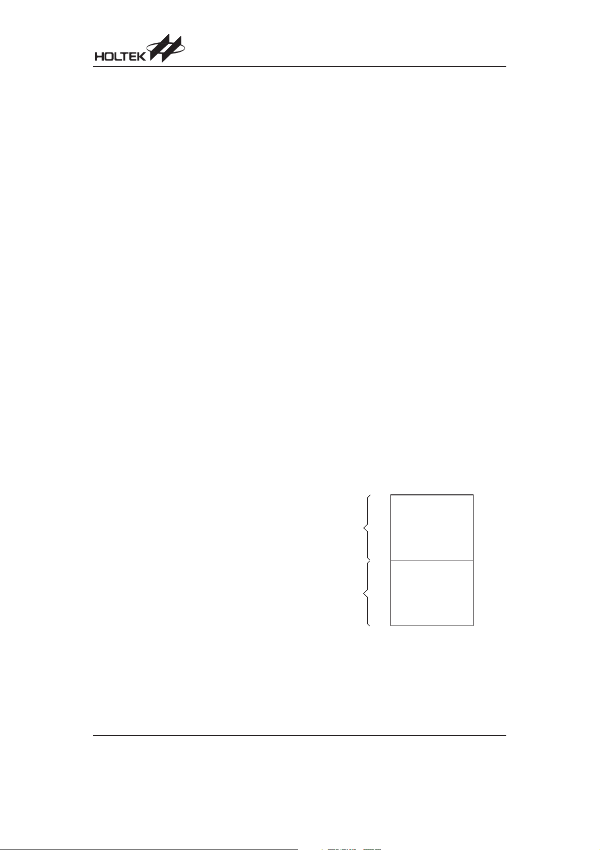
P r o g r a m
M e m o r y
P r o g r a m C o n t e r
H i g h B y t e
T B L P
T B L H S p e c i f i e d b y [ m ]
T a b l e C o n t e n t s H i g h B y t e T a b l e C o n t e n t s L o w B y t e
Table Read -TBLP only
P r o g r a m
M e m o r y
T B L H S p e c i f i e d b y [ m ]
H i g h B y t e o f T a b l e C o n t e n t s L o w B y t e o f T a b l e C o n t e n t s
T B L P
T B H P
Table Read -TBLP/TBHP

HT82B60R
Rev. 1.10 10 February 1, 2011
tempreg1 db ? ; temporary register #1
tempreg2 db ? ; temporary register #2
:
:
mov a,06h ; initialise table pointer - note that this address is referenced
mov tblp,a ; to the last page or present page
:
:
tabrdl tempreg1 ; transfers value in table referenced by table pointer to tempregl
; data at prog. memory address ²1F06H²transferred to tempreg1 and TBLH
dec tblp ; reduce value of table pointer by one
tabrdl tempreg2 ; transfers value in table referenced by table pointer to tempreg2
; data at prog.memory address ²1F05H²transferred to tempreg2 and TBLH
; in this example the data ²1AH²is transferred to
; tempreg1 and data ²0FH²to register tempreg2
; the value ²00H²will be transferred to the high byte register TBLH
:
:
org 1F00h ; sets initial address of last page
dc 00Ah, 00Bh, 00Ch, 00Dh, 00Eh, 00Fh, 01Ah, 01Bh
:
:
Because the TBLH register is a read-only register and
cannot be restored, care should be taken to ensure its
protection if both the main routine and Interrupt Service
Routine use the table read instructions. If using the table
read instructions, the Interrupt Service Routines may
change the value of TBLH and subsequently cause er-
rors if used again by the main routine. As a rule it is rec-
ommended that simultaneous use of the table read
instructions should be avoided. However, in situations
where simultaneous use cannot be avoided, the inter-
rupts should be disabled prior to the execution of any
main routine table-read instructions. Note that all table
related instructions require two instruction cycles to
complete their operation.
Data Memory
The Data Memory is a volatile area of 8-bit wide RAM
internal memory and is the location where temporary in-
formation is stored. Divided into two sections, the first of
these is an area of RAM where special function registers
are located. These registers have fixed locations and
are necessary for correct operation of the device. Many
of these registers can be read from and written to di-
rectly under program control, however, some remain
protected from user manipulation. The second area of
Data Memory is reserved for general purpose use. All
locations within this area are read and write accessible
under program control.
Structure
The two sections of Data Memory, the Special Purpose
and General Purpose Data Memory are located at con-
secutive locations. All are implemented in RAM and are
8 bits wide. The start address of the Data Memory for all
devices is the address ²00H². Registers which are com-
mon to all microcontrollers, such as ACC, PCL, etc.,
have the same Data Memory address.
General Purpose Data Memory
All microcontroller programs require an area of
read/write memory where temporary data can be stored
and retrieved for use later. It is this area of RAM memory
that is known as General Purpose Data Memory. This
area of Data Memory is fully accessible by the user pro-
gram for both read and write operations. By using the
²SET [m].i²and ²CLR [m].i²instructions, individual bits
can be set or reset under program control giving the
user a large range of flexibility for bit manipulation in the
Data Memory.
00H
28H
F F H
27H
S p e c i a l
P r p o s e
D a t a
M e m o r y
G e n e r a l
P r p o s e
D a t a
M e m o r y
Data Memory Structure
Note: Most of the Data Memory bits can be directly
manipulated using the ²SET [m].i²and ²CLR
[m].i²with the exception of a few dedicated bits.
The Data Memory can also be accessed
through the memory pointer register MP.

HT82B60R
Rev. 1.10 11 February 1, 2011
Special Purpose Data Memory
This area of Data Memory is where registers, necessary
for the correct operation of the microcontroller, are
stored. It is divided into two banks, Bank 0 and Bank1.
Most of the registers are both readable and writeable
but some are protected and are readable only, the de-
tails of which are located under the relevant Special
Function Register section. Note that for locations that
are unused, any read instruction to these addresses will
return the value ²00H².
The Special Purpose Registers for the USB interface
are stored in Bank 1 which can only be accessed by first
setting the Bank Pointer to a value of 01H and then us-
ing Indirect Addressing Register IAR1 and Memory
Pointer MP1. Bank 1 can only be accessed indirectly us-
ing the MP1 Memory Pointer, direct addressing is not
possible.
Special Function Registers
To ensure successful operation of the microcontroller,
certain internal registers are implemented in the Data
Memory area. These registers ensure correct operation
of internal functions such as timers, interrupts, etc., as
well as external functions such as I/O data control. The
location of these registers within the Data Memory be-
gins at the address 00H. Any unused Data Memory lo-
cations between these special function registers and the
point where the General Purpose Memory begins is re-
served and attempting to read data from these locations
will return a value of 00H.
Indirect Addressing Register -IAR0, IAR1
The Indirect Addressing Registers, IAR0 and IAR1, al-
though having their locations in normal RAM register
space, do not actually physically exist as normal regis-
ters. The method of indirect addressing for RAM data
manipulation uses these Indirect Addressing Registers
and Memory Pointers, in contrast to direct memory ad-
dressing, where the actual memory address is speci-
fied. Actions on the IAR0 and IAR1 registers will result in
no actual read or write operation to these registers but
rather to the memory location specified by their corre-
sponding Memory Pointer, MP0 or MP1. Acting as a
pair, IAR0 and MP0 can together only access data from
Bank 0, while the IAR1 and MP1 register pair can ac-
cess data from both Bank 0 and Bank 1. As the Indirect
Addressing Registers are not physically implemented,
reading the Indirect Addressing Registers indirectly will
return a result of ²00H²and writing to the registers indi-
rectly will result in no operation.
Memory Pointer -MP0, MP1
For all devices, two Memory Pointers, known as MP0
and MP1 are provided. These Memory Pointers are
physically implemented in the Data Memory and can be
manipulated in the same way as normal registers pro-
viding a convenient way with which to address and track
data. When any operation to the relevant Indirect Ad-
dressing Registers is carried out, the actual address that
the microcontroller is directed to, is the address speci-
fied by the related Memory Pointer. MP0 can only ac-
cess data in Bank 0 while MP1 can access both banks.
00H
01H
02H
03H
04H
05H
06H
07H
08H
09H
0 A H
0 B H
0 C H
0 D H
0 E H
0 F H
10H
11H
12H
13H
14H
15H
16H
17H
18H
19H
1 A H
1 B H
1 C H
1 D H
1 E H
1 F H
20H
21H
22H
23H
24H
25H
26H
27H
: U n s e d r e a d a s " 0 "
I A R 0
M P 0
I A R 1
M P 1
B P
A C C
P C L
T B L P
T B L H
W D T S
S T A T U S
I N T C 0
T M R 0
T M R 0 C
T M R 1 H
T M R 1 L
T M R 1 C
P A
PAC
P B
PBC
P C
P C C
P D
P D C
P E
PEC
P F
P F C
I N T C 1
T B H P
U S C
U S R
S C C
L C D C
S I M C T L 0
S I M C T L 1
S I M D I R
S I M A R / S I M C T L 2
40H
41H
42H
43H
44H
45H
46H
47H
48H
49H
4 A H
4 B H
U S B _ S T A T
P I P E _ C T R L
A W R
S T A L L
P I P E
S I E S
M I S C
E N D P T _ E N
F I F O 0
F I F O 1
F I F O 2
F I F O 3
B a n k 0 B a n k 1
Special Purpose Data Memory

HT82B60R
Rev. 1.10 12 February 1, 2011
data .section ¢data¢
adres1 db ?
adres2 db ?
adres3 db ?
adres4 db ?
block db ?
code .section at 0 ¢code¢
org 00h
start:
mov a,04h ; setup size of block
mov block,a
mov a,offset adres1 ; Accumulator loaded with first RAM address
mov mp0,a ; setup memory pointer with first RAM address
loop:
clr IAR0 ; clear the data at address defined by MP0
inc mp0 ; increment memory pointer
sdz block ; check if last memory location has been cleared
jmp loop
continue:
The important point to note here is that in the example shown above, no reference is made to specific Data Memory ad-
dresses.
Accumulator -ACC
The Accumulator is central to the operation of any
microcontroller and is closely related with operations
carried out by the ALU. The Accumulator is the place
where all intermediate results from the ALU are stored.
Without the Accumulator it would be necessary to write
the result of each calculation or logical operation such
as addition, subtraction, shift, etc., to the Data Memory
resulting in higher programming and timing overheads.
Data transfer operations usually involve the temporary
storage function of the Accumulator; for example, when
transferring data between one user defined register and
another, it is necessary to do this by passing the data
through the Accumulator as no direct transfer between
two registers is permitted.
Program Counter Low Register -PCL
To provide additional program control functions, the low
byte of the Program Counter is made accessible to pro-
grammers by locating it within the Special Purpose area
of the Data Memory. By manipulating this register, direct
jumps to other program locations are easily imple-
mented. Loading a value directly into this PCL register
will cause a jump to the specified Program Memory lo-
cation, however, as the register is only 8-bit wide, only
jumps within the current Program Memory page are per-
mitted. When such operations are used, note that a
dummy cycle will be inserted.
Look-up Table Registers -TBLP, TBLH, TBHP
These two special function registers are used to control
operation of the look-up table which is stored in the Pro-
gram Memory. TBLP and TBHP are the table pointers and
indicate the location where the table data is located. Their
value must be setup before any table read commands are
executed. Their values can be changed, for example using
the ²INC²or ²DEC²instructions, allowing for easy table
data pointing and reading. TBLH is the location where the
high order byte of the table data is stored after a table read
data instruction has been executed.
Watchdog Timer Register -WDTS
The Watchdog feature of the microcontroller provides
an automatic reset function giving the microcontroller a
means of protection against spurious jumps to incorrect
Program Memory addresses. To implement this, a timer
is provided within the microcontroller which will issue a
reset command when its value overflows. To provide
variable Watchdog Timer reset times, the Watchdog
Timer clock source can be divided by various division ra-
tios, the value of which is set using the WDTS register.
By writing directly to this register, the appropriate divi-
sion ratio for the Watchdog Timer clock source can be
setup. Note that only the lower 3 bits are used to set divi-
sion ratios between 1 and 128.
Status Register -STATUS
This 8-bit register contains the zero flag (Z), carry flag
(C), auxiliary carry flag (AC), overflow flag (OV), power
down flag (PDF), and watchdog time-out flag (TO).
These arithmetic/logical operation and system manage-
ment flags are used to record the status and operation of
the microcontroller.
With the exception of the TO and PDF flags, bits in the
status register can be altered by instructions like most
other registers. Any data written into the status register
will not change the TO or PDF flag. In addition, opera-
tions related to the status register may give different re-
sults due to the different instruction operations. The TO
flag can be affected only by a system power-up, a WDT
time-out or by executing the ²CLR WDT²or ²HALT²in-
struction. The PDF flag is affected only by executing the
²HALT²or ²CLR WDT²instruction or during a system
power-up.

HT82B60R
Rev. 1.10 13 February 1, 2011
The Z, OV, AC and C flags generally reflect the status of
the latest operations.
·Cis set if an operation results in a carry during an ad-
dition operation or if a borrow does not take place dur-
ing a subtraction operation; otherwise C is cleared. C
is also affected by a rotate through carry instruction.
·AC is set if an operation results in a carry out of the
low nibbles in addition, or no borrow from the high nib-
ble into the low nibble in subtraction; otherwise AC is
cleared.
·Zis set if the result of an arithmetic or logical operation
is zero; otherwise Z is cleared.
·OV is set if an operation results in a carry into the high-
est-order bit but not a carry out of the highest-order bit,
or vice versa; otherwise OV is cleared.
·PDF is cleared by a system power-up or executing the
²CLR WDT²instruction. PDF is set by executing the
²HALT²instruction.
·TO is cleared by a system power-up or executing the
²CLR WDT²or ²HALT²instruction. TO is set by a
WDT time-out.
In addition, on entering an interrupt sequence or execut-
ing a subroutine call, the status register will not be
pushed onto the stack automatically. If the contents of
the status registers are important and if the interrupt rou-
tine can change the status register, precautions must be
taken to correctly save it.
Interrupt Control Registers -INTC0, INTC1
The microcontrollers provide two internal timer/event
counter overflow interrupts, one USB interrupt, a com-
bined SPI/I2C interrupt and an external pin interrupt. By
setting various bits within these registers using standard
bit manipulation instructions, the enable/disable func-
tion of each interrupt can be independently controlled. A
master interrupt bit within this register, the EMI bit, acts
like a global enable/disable and is used to set all of the
interrupt enable bits on or off. This bit is cleared when an
interrupt routine is entered to disable further interrupt
and is set by executing the ²RETI²instruction.
Timer/Event Counter Registers -
TMR0, TMR0C, TMR1H, TMR1L, TMR1C
Both devices possess a single internal 8-bit count-up
timer. An associated register known as TMR0 is the lo-
cation where the timers 8-bit value is located. This regis-
ter can also be preloaded with fixed data to allow
different time intervals to be setup. An associated con-
trol register, known as TMR0C, contains the setup infor-
mation for this timer, which determines in what mode the
timer is to be used as well as containing the timer on/off
control function.
All devices possess one internal 16-bit count-up timer.
An associated register pair known as TMR1L/TMR1H is
the location where the timer 16-bit value is located. This
register can also be preloaded with fixed data to allow
different time intervals to be setup. An associated con-
trol register, known as TMR1C, contains the setup infor-
mation for this timer, which determines in what mode the
timer is to be used as well as containing the timer on/off
control function.
Input/Output Ports and Control Registers
Within the area of Special Function Registers, the I/O
registers and and their associated control registers play
a prominent role. All I/O ports have a designated regis-
ter correspondingly labeled as PA, PB, PC, PD, PE and
PF0~PF1. These labeled I/O registers are mapped to
specific addresses within the Data Memory as shown in
the Data Memory table, which are used to transfer the
appropriate output or input data on that port. With each
I/O port there is an associated control register labeled
PAC, PBC, PCC, PDC, PEC and PFC, also mapped to
specific addresses with the Data Memory.
The control register specifies which pins of that port are
set as inputs and which are set as outputs. To setup a
pin as an input, the corresponding bit of the control reg-
ister must be set high, for an output it must be set low.
During program initialisation, it is important to first setup
the control registers to specify which pins are outputs
and which are inputs before reading data from or writing
data to the I/O ports. One flexible feature of these regis-
ters is the ability to directly program single bits using the
T O P D F O V Z A C C
S T A T U S R e g i s e r
A r i h m e i c / L o g i c O p e r a i o n F l a g s
C a r r y f l a g
A x i l i a r y c a r r y f l a g
Z e r o f l a g
O v e r f l o w f l a g
S y s e m M a n a g e m e n F l a g s
P o w e r d o w n f l a g
W a t c h d o g t i m e - o t f l a g
N o t i m p l e m e n t e d , r e a d a s " 0 "
b 7 b 0
Status Register

HT82B60R
Rev. 1.10 14 February 1, 2011
²SET [m].i²and ²CLR [m].i²instructions. The ability to
change I/O pins from output to input and vice versa by
manipulating specific bits of the I/O control registers dur-
ing normal program operation is a useful feature of
these devices.
Bank Pointer -BP
The Special Purpose Data Memory is divided into two
Banks, Bank 0 and Bank 1. The USB control registers
are located in Bank 1, while all other registers are lo-
cated in Bank 1. The Bank Pointer selects which bank
data is to be accessed from. If Bank 0 is to be accessed
then BP must be set to a value of 00H, while if Bank 1 is
to be accessed then BP must be set to a value of 01H.
Serial Interface Registers
The device contains two serial interfaces, an SPI and an
I2C interface. The SIMCTL0, SIMCTL1, SIMCTL2 and
SIMAR are the control registers for the Serial Interface
function while the SIMDR is the data register for the Se-
rial Interface Data.
Software COM Register -SCOMC
The pins PC0~PC3 on Port C can be used as COM lines
to drive an external LCD panel. To implement this func-
tion, the LCDC register is used to setup the correct bias
voltages on these pins.
Input/Output Ports
Holtek microcontrollers offer considerable flexibility on
their I/O ports. With the input or output designation of ev-
ery pin fully under user program control, pull-high op-
tions for all ports and wake-up options on certain pins,
the user is provided with an I/O structure to meet the
needs of a wide range of application possibilities.
Depending upon which package is chosen, the
microcontroller provides up to 42 bidirectional input/out-
put lines labeled with port names PA, PB, PC, PD, PE
and PF0~PF1.
These I/O ports are mapped to the Data Memory with
addresses as shown in the Special Purpose Data Mem-
ory table. For input operation, these ports are non-latch-
ing, which means the inputs must be ready at the T2
rising edge of instruction ²MOV A,[m]², where m de-
notes the port address. For output operation, all the data
is latched and remains unchanged until the output latch
is rewritten.
Pull-high Resistors
Many product applications require pull-high resistors for
their switch inputs usually requiring the use of an exter-
nal resistor. To eliminate the need for these external re-
sistors, I/O pins, when configured as an input have the
capability of being connected to an internal pull-high re-
sistor. The pull-high resistors are selectable via configu-
ration options and are implemented using weak PMOS
transistors. A pin or nibble option on the I/O ports can be
selected to select pull-high Resistors.
Port A CMOS/NMOS/PMOS Structure
The pins on Port A can be setup via configuration option
to be either CMOS, NMOS or PMOS types.
Port B VDD/V33O Option Structure
The power supply for the Port B pins can be setup via
configuration option to be either VDD or V33O.
Port Pin Wake-up
If the HALT instruction is executed, the device will enter
the Power Down Mode, where the system clock will stop
resulting in power being conserved, a feature that is im-
portant for battery and other low-power applications.
Various methods exist to wake-up the microcontroller,
one of which is to change the logic condition on one of
the port pins from high to low. After a HALT instruction
forces the microcontroller into entering the Power Down
Mode, the processor will remain in a low-power state un-
til the logic condition of the selected wake-up pin on the
port pin changes from high to low. This function is espe-
cially suitable for applications that can be woken up via
external switches. Each pin on PA, PB, PC, PD, PE and
PF0~PF1 has the capability to wake-up the device on an
external falling edge. Note that some pins can only be
setup nibble wide whereas other can be bit selected to
have a wake-up function.
I/O Port Control Registers
Each I/O port has its own control register PAC, PBC,
PCC, PDC, PEC and PFC, to control the input/output
configuration. With this control register, each CMOS out-
put or input with or without pull-high resistor structures
can be reconfigured dynamically under software control.
Each of the I/O ports is directly mapped to a bit in its asso-
ciated port control register. Note that several pins can be
setup to have NMOS outputs using configuration options.
For the I/O pin to function as an input, the corresponding
bit of the control register must be written as a ²1². This
will then allow the logic state of the input pin to be di-
rectly read by instructions. When the corresponding bit
of the control register is written as a ²0², the I/O pin will
be setup as an output. If the pin is currently setup as an
output, instructions can still be used to read the output
register. However, it should be noted that the program
B a n k P o i n e r
b 7 b 0
BP0
B P 0 D a t a M e m o r y
0 B a n k 0
1 B a n k 1
N o t s e d , m s t b e r e s e t t o " 0 "
Bank Pointer

HT82B60R
Rev. 1.10 15 February 1, 2011
will in fact only read the status of the output data latch
and not the actual logic status of the output pin.
Pin-shared Functions
The flexibility of the microcontroller range is greatly en-
hanced by the use of pins that have more than one func-
tion. Limited numbers of pins can force serious design
constraints on designers but by supplying pins with
multi-functions, many of these difficulties can be over-
come. For some pins, the chosen function of the
multi-function I/O pins is set by configuration options
while for others the function is set by application pro-
gram control.
·External Interrupt Input
The external interrupt pin, INT is pin-shared with the
I/O pin PB5. For applications not requiring an external
interrupt input, the pin-shared external interrupt pin
can be used as a normal I/O pin, however to do this,
the external interrupt enable bit in the INTC1 register
must be disabled.
·External Timer0 Clock Input
The external timer pin TMR0 is pin-shared with the I/O
pin PA6. To configure this pin to operate as timer input,
the corresponding control bits in the timer control reg-
ister must be correctly set. For applications that do not
require an external timer input, this pin can be used as
a normal I/O pin. Note that if used as a normal I/O pin
the timer mode control bits in the timer control register
must select the timer mode, which has an internal
clock source, to prevent the input pin from interfering
with the timer operation.
·External Timer1 Clock Input
The external timer pin TMR1 is pin-shared with the I/O
pin PA7. To configure this pin to operate as timer input,
the corresponding control bits in the timer control reg-
ister must be correctly set. For applications that do not
require an external timer input, this pin can be used as
a normal I/O pin. Note that if used as a normal I/O pin
the timer mode control bits in the timer control register
must select the timer mode, which has an internal
clock source, to prevent the input pin from interfering
with the timer operation.
External Interrupt Input
The external interrupt pin INT is pin-shared with the I/O
pin PB5. For applications not requiring an external inter-
rupt input, the pin-shared external interrupt pin can be
used as a normal I/O pin, however to do this, the exter-
nal interrupt enable bits in the INTC1 register must be
disabled.
COM Driver Pins
Pins PC0~PC3 on Port C can be used as LCD COM
driver pins. This function is controlled using the LCDC
register which will generate the necessary 1/2 bias sig-
nals on these four pins.
Serial Interface Module
The device pins, PB0~PB3, are pin-shared with pins
SDA, SCL, SCS, SCK, SDI, SDO. The choice of which
function is used is selected using the SIMCTL0 register.
I/O Pin Structures
The diagram illustrates a generic I/O pin internal struc-
tures. As the exact logical construction of the I/O pin will
differ and as the pin-shared structures are not illustrated
this diagram is supplied as a guide only to assist with the
functional understanding of the I/O pins.
Programming Considerations
Within the user program, one of the first things to con-
sider is port initialisation. After a reset, all of the data and
port control register will be set high. This means that all
I/O pins will default to an input state, the level of which
depends on the other connected circuitry and whether
pull-high options have been selected. If the PAC, PBC,
VD D / V 3 3 O ( P B )
M
U
X
W a k e - p O p t i o n
S y s t e m W a k e - p
R e a d D a t a R e g i s t e r
DQ
C K
S
DQ
C K
S
C o n t r o l B i t
D a t a B s
W r i t e C o n t r o l R e g i s t e r
C h i p R e s e t
R e a d C o n t r o l R e g i s t e r
W r i t e D a t a R e g i s t e r
D a t a B i t
I / O p i n
Q
Q
W e a k
P l l - p
P l l - H i g h
O p t i o n
Input/Output Ports

HT82B60R
Rev. 1.10 16 February 1, 2011
PCC, PDC, PEC and PFC port control register, are then
programmed to setup some pins as outputs, these out-
put pins will have an initial high output value unless the
associated PA, PB, PC, PD, PE and PF port data regis-
ters are first programmed. Selecting which pins are in-
puts and which are outputs can be achieved byte-wide
by loading the correct value into the port control register
or by programming individual bits in the port control reg-
ister using the ²SET [m].i²and ²CLR [m].i²instructions.
Note that when using these bit control instructions, a
read-modify-write operation takes place. The
microcontroller must first read in the data on the entire
port, modify it to the required new bit values and then re-
write this data back to the output ports.
All pins have the additional capability of providing
wake-up functions. When the device is in the Power
Down Mode, various methods are available to wake the
device up. One of these is a high to low transition of any
of the Port pins. Single or multiple pins can be setup to
have this function.
Timer/Event Counters
The provision of timers form an important part of any
microcontroller, giving the designer a means of carrying
out time related functions. This device contains two
count-up timers of 8-bit and 16-bit capacities respec-
tively. As each timer has three different operating
modes, they can be configured to operate as a general
timer, an external event counter or as a pulse width
measurement device.
There are two types of registers related to the
Timer/Event Counters. The first is the register that con-
tains the actual value of the Timer/Event Counter and
into which an initial value can be preloaded, and is
known as TMR0, TMR1H or TMR1L. Reading from this
register retrieves the contents of the Timer/Event Coun-
ter. The second type of associated register is the Timer
Control Register, which defines the timer options and
determines how the Timer/Event Counter is to be used,
and has the name TMR0C or TMR1C. This device can
have the timer clocks configured to come from the inter-
nal clock sources. In addition, the timer clock source can
also be configured to come from the external timer pins.
The external clock source is used when the Timer/Event
Counter is in the event counting mode, the clock source
being provided on the external timer pin. The pin has the
name TMR0 or TMR1 and is pin-shared with an I/O pin.
Depending upon the condition of the T0E or T1E bit in
the Timer Control Register, each high to low, or low to
high transition on the external timer input pin will incre-
ment the Timer/Event Counter by one.
Configuring the Timer/Event Counter Input Clock
Source
The Timer/Event Counter¢s clock can originate from var-
ious sources. The system clock source is used when the
Timer/Event Counter 0 is in the timer mode or in the
pulse width measurement mode. The instruction clock
source (system clock source divided by 4) is used when
the Timer/Event Counter 1 is in the timer mode or in the
pulse width measurement mode. The external clock
source is used when the Timer/Event Counter is in the
event counting mode, the clock source being provided
on the external timer pin, TMR0 or TMR1. Depending
upon the condition of the T0E or T1E bit, each high to
low, or low to high transition on the external timer pin will
increment the counter by one.
Timer Register -TMR0, TMR1L/TMR1H
The timer registers are special function registers located
in the Special Purpose RAM Data Memory and are the
places where the actual timer values are stored. For
8-bit Timer/Event Counter 0, this register is known as
TMR0. For 16-bit Timer/Event Counter 1, the timer reg-
isters are known as TMR1L and TMR1H. The value in
the timer registers increases by one each time an inter-
nal clock pulse is received or an external transition oc-
curs on the external timer pin. The timer will count from
the initial value loaded by the preload register to the full
count of FFH for the 8-bit timer or FFFFH for the 16-bit
timer at which point the timer overflows and an internal
interrupt signal is generated. The timer value will then
be reset with the initial preload register value and con-
tinue counting.
To achieve a maximum full range count of FFH for the
8-bit timer or FFFFH for the 16-bit timer, the preload reg-
isters must first be cleared to all zeros. It should be
noted that after power-on, the preload register will be in
an unknown condition. Note that if the Timer/Event
Counter is switched off and data is written to its preload
registers, this data will be immediately written into the
actual timer registers. However, if the Timer/Event
Counter is enabled and counting, any new data written
into the preload data registers during this period will re-
main in the preload registers and will only be written into
the timer registers the next time an overflow occurs.
For the 16-bit Timer/Event Counter which has both low
byte and high byte timer registers, accessing these reg-
isters is carried out in a specific way. It must be note
when using instructions to preload data into the low byte
timer register, namely TMR1L, the data will only be
placed in a low byte buffer and not directly into the low
byte timer register. The actual transfer of the data into
T 1 T 2 T 3 T 4 T 1 T 2 T 3 T 4
W r i t e t o P o r t R e a d f r o m P o r t
S y s t e m C l o c k
P o r t D a t a
Read/Write Timing

HT82B60R
Rev. 1.10 17 February 1, 2011
b 7
T 0 O NT 0 M 0T 0 M 1
b 0
T M R 0 C R e g i s e r
T 0 M 1
0
0
1
1
T 0 M 0
0
1
0
1
T 0 E
N o t i m p l e m e n t e d , r e a d a s " 0 "
T i m e r / E v e n t C o n t e r 0 a c t i v e e d g e s e l e c t
1 : c o n t o n f a l l i n g e d g e
0 : c o n t o n r i s i n g e d g e
T i m e r / E v e n t C o n t e r 0 C o n t i n g E n a b l e
1: enable
0 : d i s a b l e
N o t i m p l e m e n t e d , r e a d a s " 0 "
O p e r a t i n g M o d e S e l e c t
no m ode available
e v e n t c o n t e r m o d e
t i m e r m o d e
p l s e w i d t h m e a s r e m e n t m o d e
Timer/Event Counter 0 Control Register
T M R 0
T 0 E
T i m e r / E v e n t C o n t e r
M o d e C o n t r o l
T 0 O N
P r e l o a d R e g i s t e r
T i m e r / E v e n t
C o n t e r
D a t a B s
R e l o a d
O v e r f l o w
t o I n t e r r p t
8 - B i t T i m e r / E v e n t C o n t e r
T 0 M 1 T 0 M 0
fSYS/ 4
8-bit Timer/Event Counter 0 Structure
T M R 1
T 1 E
T i m e r / E v e n t C o n t e r
M o d e C o n t r o l
1 6 - B i t
P r e l o a d R e g i s t e r
D a t a B s
R e l o a d
O v e r f l o w
t o I n t e r r p t
L o w B y t e
B f f e r
T 1 M 1 T 1 M 0
T 1 O N
H i g h B y t e L o w B y t e
1 6 - B i t T i m e r / E v e n t C o n t e r
f
SYS
/ 4
16-bit Timer/Event Counter 1 Structure
b 7
T 1 O NT 1 M 0T 1 M 1
b 0
T M R 1 C R e g i s e r
T 1 M 1
0
0
1
1
T 1 M 0
0
1
0
1
T 1 E
N o t i m p l e m e n t e d , r e a d a s " 0 "
T i m e r / E v e n t C o n t e r 1 a c t i v e e d g e s e l e c t
1 : c o n t o n f a l l i n g e d g e
0 : c o n t o n r i s i n g e d g e
T i m e r / E v e n t C o n t e r 1 c o n t i n g e n a b l e
1: enable
0 : d i s a b l e
N o t i m p l e m e n t e d , r e a d a s " 0 "
O p e r a t i n g m o d e s e l e c t
no m ode available
e v e n t c o n t e r m o d e
t i m e r m o d e
p l s e w i d t h m e a s r e m e n t m o d e
Timer/Event Counter 1 Control Register

HT82B60R
Rev. 1.10 18 February 1, 2011
the low byte timer register is only carried out when a
write to its associated high byte timer register, namely
TMR1H, is executed. On the other hand, using instruc-
tions to preload data into the high byte timer register will
result in the data being directly written to the high byte
timer register. At the same time the data in the low byte
buffer will be transferred into its associated low byte
timer register. For this reason, the low byte timer regis-
ter should be written first when preloading data into the
16-bit timer registers. It must also be noted that to read
the contents of the low byte timer register, a read to the
high byte timer register must be executed first to latch
the contents of the low byte timer register into its associ-
ated low byte buffer. After this has been done, the low
byte timer register can be read in the normal way. Note
that reading the low byte timer register will result in read-
ing the previously latched contents of the low byte buffer
and not the actual contents of the low byte timer register.
Timer Control Register -TMR0C/TMR1C
The flexible features of the Holtek microcontroller
Timer/Event Counters enable them to operate in three
different modes, the options of which are determined by
the contents of their respective control register. For de-
vices are two timer control registers known as TMR0C,
TMR1C . It is the timer control register together with its
corresponding timer registers that control the full opera-
tion of the Timer/Event Counters. Before the timers can
be used, it is essential that the appropriate timer control
register is fully programmed with the right data to ensure
its correct operation, a process that is normally carried
out during program initialization.
To choose which of the three modes the timer is to oper-
ate in, either in the timer mode, the event counting mode
or the pulse width measurement mode, bits 7 and 6 of
the Timer Control Register, which are known as the bit
pair T0M1/T0M0 or T1M1/T1M0 respectively, depend-
ing upon which timer is used, must be set to the required
logic levels. The timer-on bit, which is bit 4 of the Timer
Control Register and known as T0ON or T1ON, depend-
ing upon which timer is used, provides the basic on/off
control of the respective timer. Setting the bit high allows
the counter to run, clearing the bit stops the counter. If
the timer is in the event count or pulse width measure-
ment mode, the active transition edge level type is se-
lected by the logic level of bit 3 of the Timer Control
Register which is known as T0E or T1E, depending
upon which timer is used.
Configuring the Timer Mode
In this mode, the Timer/Event Counter can be utilised to
measure fixed time intervals, providing an internal inter-
rupt signal each time the Timer/Event Counter over-
flows. To operate in this mode, the Operating Mode
Select bit pair, T0M1/T0M0 or T1M1/T1M0, in the Timer
Control Register must be set to the correct value as
shown.
Control Register Operating Mode
Select Bits for the Timer Mode
Bit7 Bit6
10
In this mode the internal clock, fSYS/4 is used as the inter-
nal clock for the Timer/Event Counters. After the other
bits in the Timer Control Register have been setup, the
enable bit T0ON or T1ON, which is bit 4 of the Timer
Control Register, can be set high to enable the
Timer/Event Counter to run.Each time an internal clock
cycle occurs, the Timer/Event Counter increments by
one. When it is full and overflows, an interrupt signal is
generated and the Timer/Event Counter will reload the
value already loaded into the preload register and con-
tinue counting. The interrupt can be disabled by ensur-
ing that the Timer/Event Counter Interrupt Enable bit in
the Interrupt Control Register, INTC0, is reset to zero.
Configuring the Event Counter Mode
In this mode, a number of externally changing logic
events, occurring on the external timer pin, can be re-
corded by the Timer/Event Counter. To operate in this
mode, the Operating Mode Select bit pair, T0M1/T0M0
or T1M1/T1M0, in the Timer Control Register must be
set to the correct value as shown.
Control Register Operating Mode
Select Bits for the Event Counter Mode
Bit7 Bit6
01
I n c r e m e n t
T i m e r C o n t r o l l e r
P r e s c a l e r O t p t
T i m e r + 1 T i m e r + 2 T i m e r + N T i m e r + N + 1
Timer Mode Timing Chart
T i m e r + 2
E x t e r n a l E v e n t
I n c r e m e n t
T i m e r C o n t e r T i m e r + 3T i m e r + 1
Event Counter Mode Timing Chart

HT82B60R
Rev. 1.10 19 February 1, 2011
In this mode, the external timer pin, TMR0 or TMR1, is
used as the Timer/Event Counter clock source, however
it is not divided by the internal prescaler. After the other
bits in the Timer Control Register have been setup, the
enable bit T0ON or T1ON, which is bit 4 of the Timer
Control Register, can be set high to enable the
Timer/Event Counter to run. If the Active Edge Select bit
T0E or T1E, which is bit 3 of the Timer Control Register,
is low, the Timer/Event Counter will increment each time
the external timer pin receives a low to high transition. If
the Active Edge Select bit is high, the counter will incre-
ment each time the external timer pin receives a high to
low transition. When it is full and overflows, an interrupt
signal is generated and the Timer/Event Counter will re-
load the value already loaded into the preload register
and continue counting. The interrupt can be disabled by
ensuring that the Timer/Event Counter Interrupt Enable
bit in the Interrupt Control Register, INTC0, is reset to
zero.
As the external timer pin is shared with an I/O pin, to en-
sure that the pin is configured to operate as an event
counter input pin, two things have to happen. The first is
to ensure that the Operating Mode Select bits in the
Timer Control Register place the Timer/Event Counter in
the Event Counting Mode, the second is to ensure that
the port control register configures the pin as an input. It
should be noted that in the event counting mode, even if
the microcontroller is in the Power Down Mode, the
Timer/Event Counter will continue to record externally
changing logic events on the timer input pin. As a result
when the timer overflows it will generate a timer interrupt
and corresponding wake-up source.
Configuring the Pulse Width Measurement Mode
In this mode, the Timer/Event Counter can be utilised to
measure the width of external pulses applied to the ex-
ternal timer pin. To operate in this mode, the Operating
Mode Select bit pair, T0M1/T0M0 or T1M1/T1M0, in the
Timer Control Register must be set to the correct
valueas shown.
Control Register Operating Mode Select
Bits for the Pulse Width Measurement Mode
Bit7 Bit6
11
In this mode the internal clock, fSYS/4 is used as the inter-
nal clock for the Timer/Event Counters. After the other
bits in the Timer Control Register have been setup, the
enable bit T0ON or T1ON, which is bit 4 of the Timer
Control Register, can be set high to enable the
Timer/Event Counter, however it will not actually start
counting until an active edge is received on the external
timer pin.
If the Active Edge Select bit T0E or T1E, which is bit 3 of
the Timer Control Register, is low, once a high to low
transition has been received on the external timer pin,
TMR0 or TMR1, the Timer/Event Counter will start
counting until the external timer pin returns to its original
high level. At this point the enable bit will be automati-
cally reset to zero and the Timer/Event Counter will stop
counting. If the Active Edge Select bit is high, the
Timer/Event Counter will begin counting once a low to
high transition has been received on the external timer
pin and stop counting when the external timer pin re-
turns to its original low level. As before, the enable bit
will be automatically reset to zero and the Timer/Event
Counter will stop counting. It is important to note that in
the Pulse Width Measurement Mode, the enable bit is
automatically reset to zero when the external control
signal on the external timer pin returns to its original
level, whereas in the other two modes the enable bit can
only be reset to zero under program control.
The residual value in the Timer/Event Counter, which
can now be read by the program, therefore represents
the length of the pulse received on the external timer
pin. As the enable bit has now been reset, any further
transitions on the external timer pin will be ignored. Not
until the enable bit is again set high by the program can
the timer begin further pulse width measurements. In
this way, single shot pulse measurements can be easily
made.
It should be noted that in this mode the Timer/Event
Counter is controlled by logical transitions on the exter-
nal timer pin and not by the logic level. When the
Timer/Event Counter is full and overflows, an interrupt
signal is generated and the Timer/Event Counter will re-
load the value already loaded into the preload register
and continue counting. The interrupt can be disabled by
+ 1 + 2 + 3 + 4
T i m e r
E x t e r n a l T i m e r
P i n I n p t
T 0 O N o r T 1 O N
( w i t h T 0 E o r T 1 E = 0 )
P r e s c a l e r O t p t
I n c r e m e n t
T i m e r C o n t e r
P r e s c a l e r O t p t i s s a m p l e d a t e v e r y f a l l i n g e d g e o f T 1 .
Pulse Width Measure Mode Timing Chart

HT82B60R
Rev. 1.10 20 February 1, 2011
ensuring that the Timer/Event Counter Interrupt Enable
bit in the Interrupt Control Register, INTC0, is reset to
zero.
As the external timer pin is shared with an I/O pin, to en-
sure that the pin is configured to operate as a pulse
width measurement pin, two things have to happen. The
first is to ensure that the Operating Mode Select bits in
the Timer Control Register place the Timer/Event Coun-
ter in the Pulse Width Measurement Mode, the second
is to ensure that the port control register configures the
pin as an input.ot by the logic level.
I/O Interfacing
The Timer/Event Counter, when configured to run in the
event counter or pulse width measurement mode, re-
quire the use of the external TMR0 and TMR1 pins for
correct operation. As these pins are shared pins they
must be configured correctly to ensure they are setup
for use as Timer/Event Counter inputs and not as a nor-
mal I/O pins. This is implemented by ensuring that the
mode select bits in the Timer/Event Counter control reg-
ister, select either the event counter or pulse width mea-
surement mode. Additionally the Port Control Register
bits for these pins must be set high to ensure that the pin
is setup as an input. Any pull-high resistor configuration
option on these pins will remain valid even if the pin is
used as a Timer/Event Counter input.
Programming Considerations
When configured to run in the timer mode, the internal
system clock is used as the timer clock source and is
therefore synchronised with the overall operation of the
microcontroller. In this mode when the appropriate timer
register is full, the microcontroller will generate an internal
interrupt signal directing the program flow to the respec-
tive internal interrupt vector. For the pulse width mea-
surement mode, the internal system clock is also used as
the timer clock source but the timer will only run when the
correct logic condition appears on the external timer input
pin. As this is an external event and not synchronised
with the internal timer clock, the microcontroller will only
see this external event when the next timer clock pulse
arrives. As a result, there may be small differences in
measured values requiring programmers to take this into
account during programming. The same applies if the
timer is configured to be in the event counting mode,
which again is an external event and not synchronised
with the internal system or timer clock.
When the Timer/Event Counter is read, or if data is writ-
ten to the preload register, the clock is inhibited to avoid
errors, however as this may result in a counting error,
this should be taken into account by the programmer.
Care must be taken to ensure that the timers are prop-
erly initialised before using them for the first time. The
associated timer enable bits in the interrupt control reg-
ister must be properly set otherwise the internal interrupt
associated with the timer will remain inactive. The edge
select, timer mode and clock source control bits in timer
control register must also be correctly set to ensure the
timer is properly configured for the required application.
It is also important to ensure that an initial value is first
loaded into the timer registers before the timer is
switched on; this is because after power-on the initial
values of the timer registers are unknown. After the
timer has been initialised the timer can be turned on and
off by controlling the enable bit in the timer control regis-
ter. Note that setting the timer enable bit high to turn the
timer on, should only be executed after the timer mode
bits have been properly setup. Setting the timer enable
bit high together with a mode bit modification, may lead
to improper timer operation if executed as a single timer
control register byte write instruction.
When the Timer/Event counter overflows, its corre-
sponding interrupt request flag in the interrupt control
register will be set. If the timer interrupt is enabled this
will in turn generate an interrupt signal. However irre-
spective of whether the interrupts are enabled or not, a
Timer/Event counter overflow will also generate a
wake-up signal if the device is in a Power-down condi-
tion. This situation may occur if the Timer/Event Counter
is in the Event Counting Mode and if the external signal
continues to change state. In such a case, the
Timer/Event Counter will continue to count these exter-
nal events and if an overflow occurs the device will be
woken up from its Power-down condition. To prevent
such a wake-up from occurring, the timer interrupt re-
quest flag should first be set high before issuing the
²HALT²instruction to enter the Power Down Mode.
Timer Program Example
This program example shows how the Timer/Event
Counter registers are setup, along with how the inter-
rupts are enabled and managed. Note how the
Timer/Event Counter is turned on, by setting bit 4 of the
Timer Control Register. The Timer/Event Counter can
be turned off in a similar way by clearing the same bit.
This example program sets the Timer/Event Counter to
be in the timer mode, which uses the internal system
clock as the clock source.
Table of contents
Other Holtek Recording Equipment manuals