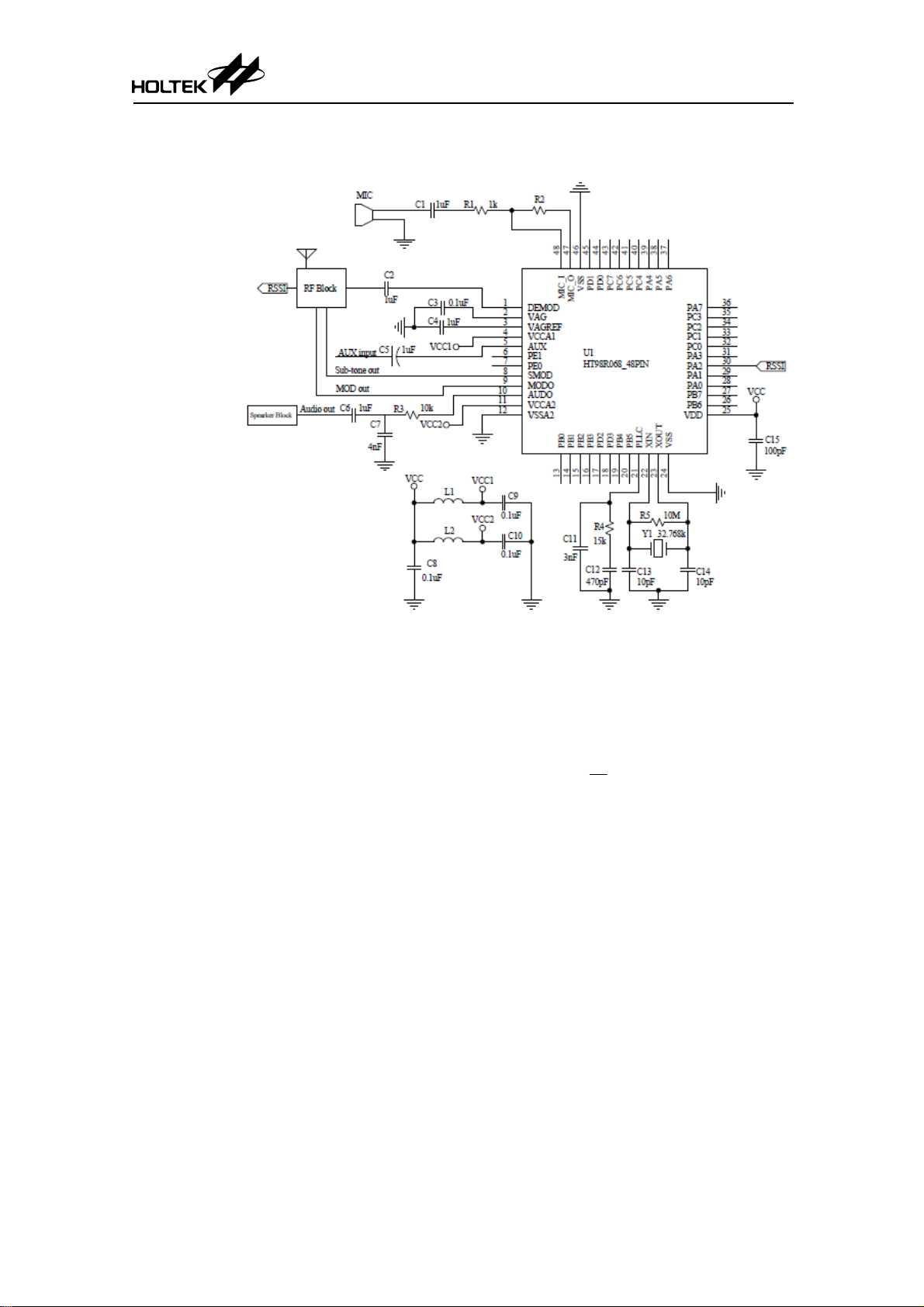
HT98R068 Two-way Radio MCU
System Clock Switches
Controlled by two registers: CTRL2[7-5,3-0] and CTRL0[0]. The description is as follows:
System Control register 2 (CTRL2)
Bit # 7 6 5 4 3 2 1 0
CTRL2 M1 M0 PLLD2 AUPRST PLLEN PLLD1 PLLD0 LXTEN
POR 0 0 1 0 0 1 1 0
CTRL2[3]:This bit controls the PLL on/off function. The CTRL2[7-6] bits select the PLL
output frequency which has four system frequencies to meet different application
requirements. The CTRL2[5] bit selects the PLL divider magnification of the audio
processor with one and two times provided. The CTRL2[2-1] bit is the PLL divider/multiply
select bits of the MCU with 1, 2, 4 ratio selections. The CTRL2[0] bit is the LXT oscillator
on/off control, which when used together with the HALT instruction, can request the
system to enter the IDLE MODE.
System Control register 0 (CTRL0)
Bit No. 7 6 5 4 3 2 1 0
CTRL0 PCFG PFDCS - - - PFDC LXTLP CLKMOD
POR 0 0 0 0 0 0 0 1
The CTRL0[0] bit selects the MCU speed mode. If CTRL0[0]=1, the MCU operates in the
low speed mode (32.768kHz.) If CTRL0[0]=0, the MCU operates in the PLL mode. When
using the PLL mode, it is important to note that when the PLL is enabled the PLL output
and audio processor divider ratio must be first selected, after which a delay of 10ms (PLL
stabilising time) must be implemented before allowing it to be a device clock source.
When the Audio processor is turned on CTRL2[4].) in the PLL mode, it is recommended
not to change the PLL divider setting.
MCU Audio processor
PLLD1 , PLLD0 PLLD2
PLLEN M1 , M0 PLL
Speed 0,1 (÷1) 1,0 (÷2) 1,1 (0,0) 0 (÷1) 1 (÷2)
0 X 32.768K 32.768K 32.768K
1 0,0 8.192M 8.192M 4.096M 2.048M 8.192M 4.096M
1 0,1 10.24M 10.24M 5.12M 2.56M 10.24M 5.12M
1 1,0 12.288M 12.288M 6.144M 3.072M 12.288M 6.144M
1 1,1 16.384M 16.384M 8.192M 4.096M 16.384M 8.192M
X: Don’t care.
MCU & Audio Processor PLL Divider Table
4