Holux M-9329 - User manual

No.1-1, Innovation Rd.1, HsinChu City 300, Science-based Industrial Park, aiwan
(300) 新竹市科學園區創新一路 1-1 號
EL: 03-6687000 FAX: 03-6687111
Website: www.holux.com
All Right Reserved
M-9329
SPECIFICA ION
GPS Engine Board

GPS Engine Board M-9329
- i -
Version Update History
Version
Date Revised Reason
0.1 2010/07/09
Draft release

- ii -
Tab e of Content
1. Introduction.............................................................................................1
1.1 Genera introductions .......................................................................1
1.2 Key Features......................................................................................1
1.3 App ications.......................................................................................1
2 Technica Description.............................................................................2
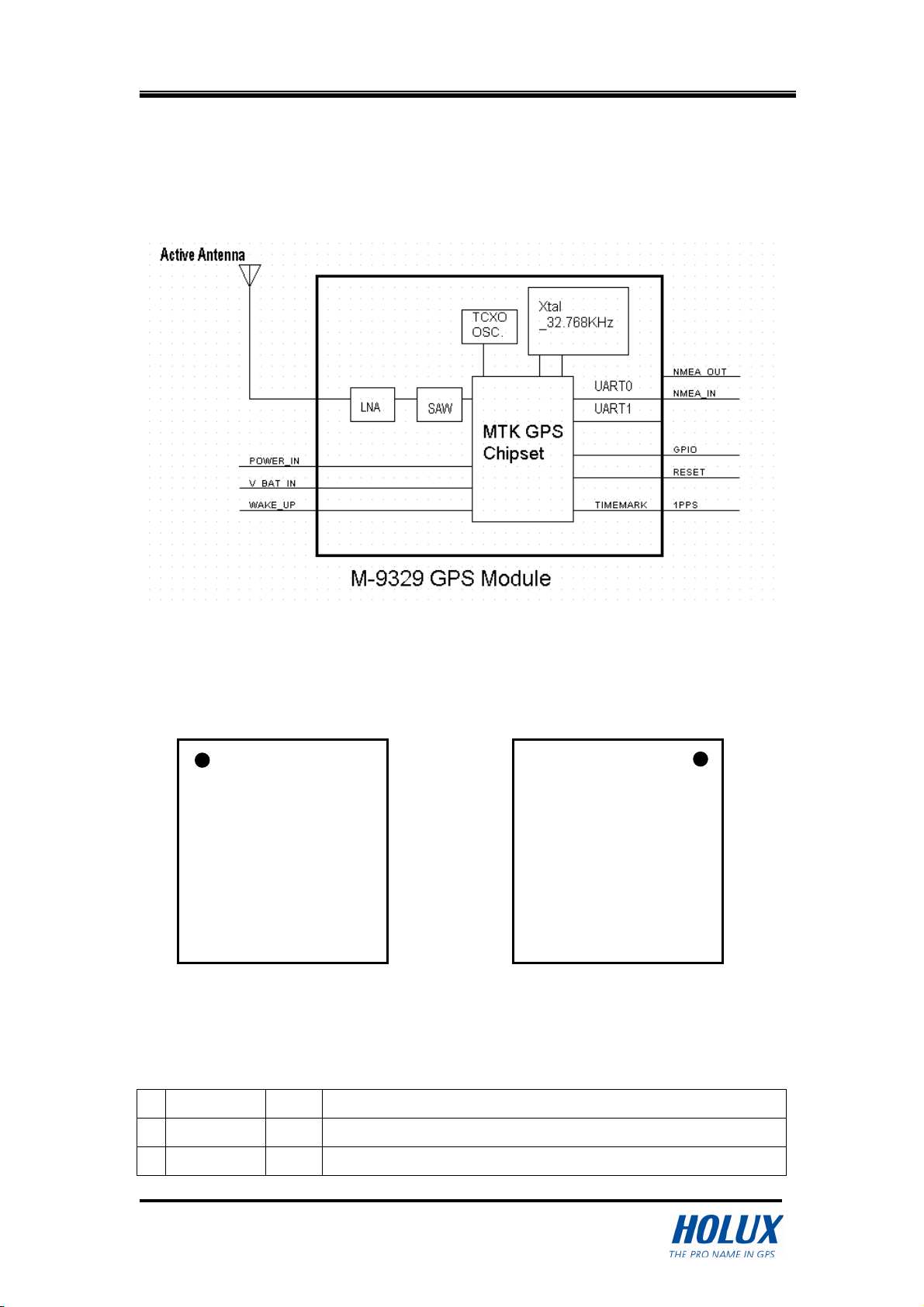
2.1 B ock Diagram ...................................................................................2
2.2 Pin Definition .....................................................................................2
2.3 Specification ......................................................................................4
3 Mechanica Dimension ...........................................................................6
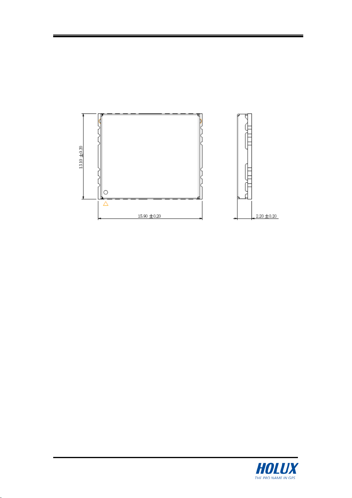
3.1 Mechanica Dimension......................................................................6
4 Package ...................................................................................................7
4.1 Packing ..............................................................................................7
4.2 Reference Product Photo.................................................................8
5. User Interface..........................................................................................9
5.1 NMEA Protoco ..................................................................................9
5.2 NMEA Protoco format......................................................................9
5.3 MTK NMEA Packet Format .............................................................10
6. Reference Design ................................................................................. 11
6.1 Reference circuit............................................................................. 11
6.2 Reference PCB pattern...................................................................12
6.3 Recommendation ref ow profi e.....................................................13

GPS Engine Board M-9329
- 1 -
1. Introduction
1.1 Genera introductions
M-9329 is an ultra miniature 13.1 * 15.9 * 2.2 mm GPS engine board
designed by low power consumption M K GPS solution. It provides
superior sensitivity up to -165dBm and fast ime- o-First-Fix in navigation
application. he stable performance of M-9329 is your best choice to be
embedded in your portable device design, like PDA、PND、mobile phone、
Digital Camera for GPS service.
1.2 Key Features
‧ small form factor:13.1* 15.9 * 2.2 mm
‧ RoHS/WEEE compliant
‧ High sensitivity -165dBm( racking , Accroding to M K chip spec)
‧ Up to 66 parallel searching,22 tracking channels
‧ Fast Position Fix
‧ Low power consumption
‧ R CM-in ready.
‧ Built-in WAAS/EGNOS/MSAS Demodulator.
‧ Support NMEA0183 V 3.01 data protocol.
‧ Real time navigation for location based services.
‧ For Car Navigation, Marine Navigation, Fleet Management, AVL and
Location-Based Services, Auto Pilot, Personal Navigation or touring
devices, racking devices/systems and Mapping devices application
1.3 App ications
‧ Automotive and Marine Navigation
‧ Automotive Navigator racking
‧ Emergency Locator
‧ Geographic Surveying
‧ Personal Positioning
‧ Sporting and Recreation
‧ Embedded applications: Smart phone, UMPC, PND, MP4

GPS Engine Board M-9329
- 2 -
2 Technica Description
2.1 B ock Diagram
2.2 Pin Definition
op view Button view
Pin
Pin Name Type
Function description
1
GPS_RF_IN
I GPS signal input(DC:2.8V output)
2
GND G Ground
30
19
11
P1
P2
P3
P4
P5
P6
P7
P8
P9
P10
P11
P29
P28
P27
P26
P25
P24
P23
P22
P21
P20
P19
P1
P2
P3
P4
P5
P6
P7
P8
P9
P10
P11
P29
P28
P27
P26
P25
P24
P23
P22
P21
P20
P19
M-93_VA1_100813
P12 P13 P14 P15 P16 P17 P18
P
36
P
35
P
3
4 P
33
P
32
P
31
P
30
P1
8
P1
7
P1
6
P15
P1
4
P1
3
P1
2
P
30
P
31
P
32
P
33
P
34
P
35
P
36

GPS Engine Board M-9329
- 3 -
3
GND G Ground
4
GND G Ground
5
V_BAT_3V3
I R C and backup SRAM , DC Input:2.8~4.2V.
NC: provide the power by module internal VCC.
6
GND G Ground
7
NC NC NC
8
GND G Ground
9
GND G Ground
10
GND G Ground
11
VCC_IN_3V3
I 3.3 ~ 4.2 VDC Power Input
12
GND G Ground
13
RESET I System Reset ,Active Low
14
GND G Ground
15
GND G Ground
16
GPIO3 I General purpose I/O
17
GND G Ground
18
GPIO1 I/O General purpose I/O
19
GND G Ground
20
1PPS O
1 PPS output pulse width 100 ms, edge tolerance is +/- 50ns.
21
GND G Ground
22
GND G Ground
23
GND G Ground
24
GND G Ground
25
GPIO2 I/O
General purpose I/O
26
GND G Ground
27
WAKE_UP
I NC,Option,the module will go to standby mode
when this pin is low
28
GND G Ground
29
GND G Ground
30
TX0 O Serial Data Output
31
RX0 I Serial Data Input
32
RX1 I Serial Data Input
33
GND G Ground
34
TX1 O Serial Data Output
35
GND G Ground
36
GND G Ground

GPS Engine Board M-9329
- 4 -
2.3 Specification
Genera (Follow M K chip specification)
GPS techno ogy M K GPS chipset M 3329
Frequency L1,1575.42MHZ
C/A Code 1.023MHZ chip rate
Channe s 66 parallel searching,22 tracking channels
Sensitivity - 165 dBm ( racking)
Receiver Accuracy (Follow M K chip specification)
Position Without aid:3.0 M 2D-RMS
DGPS(WAAS, EGNOS, MSAS, R CM):2.5 M
Ve ocity Without aid:0.1 M/sec
Time 0.1µs. Sync GPS time
Datum
Datum WGS84(Default) total 219 datum’s
Time to First Fix (Follow M K chip specification)
Hot start < 1 sec.
Warm start < 33 sec.
Co d start < 35 sec.
Reacquisition <1sec.
Protoco
GPS Output Data
NMEA0183(V3.01)-
GGA,GLL,GSA,GSV,RMC,V G
Support Baud rate 4800/9600/…./115200 bps
(default 4800), Data bit:8 , Stop bit:1, No parity.
Update Rata 1Hz(default)
Protoco Support NMEA-0183
1PPS Enable(1Hz pulse 10% duty cycle)
Limitations (Follow M K chip specification)
Acce eration Limit <4G
A titude Limit <18000 meters
Ve ocity Limit <515 M/sec
Jerk Limit 20 M/sec
3
Power
Operation Current Acquisition:≒42 [email protected]
Operation Current racking:≒<36 [email protected]

GPS Engine Board M-9329
- 5 -
DC Input Range
VCC_IN_3V3: 3.3~4.2V
V_BA _3V3:
2.0~4.2V
Processing Core
Processor Type ARM7EJ-S
Processor Speeds 48 MHz
Interface CMOS 2.8 V Level
Temperature
Operating Temperature
-30 to +80 .
Storage Temperature -40 to +85 .
Operating Humidity 5% to 95%, Non condensing
Physica
Dimension 13.1 * 15.9 * 2.2 mm.
Weight <1g.

GPS Engine Board M-9329
- 6 -
3 Mechanica Dimension
3.1 Mechanica Dimension
OP VIEW

GPS Engine Board M-9329
- 7 -
4 Package
4.1 Packing
ray dimension: 325*220*9 mm, Standard Content Qty: 100 pcs.
Carton dimension: 340*235*120 mm, Standard Content Qty: 2,000 pcs.

GPS Engine Board M-9329
- 8 -
4.2 Reference Product Photo
he photo is for reference, the real content will depend on the real
configuration.
op side:
Bottom side: ( he PCB version depend)

GPS Engine Board M-9329
- 9 -
5. User Interface
M-9329 provides 2-wire digital UAR port for communication of GPS position
data using NMEA protocol or M K extension protocol. UAR port is capable of
4800 to 115200 baud rate.
5.1 NMEA Protoco
M-9329 is default to support standard NMEA-0183 protocol. In addition, a
series of M K extensions (PM K messages) have been developed that can
be used to provide extended capabilities common to many applications.
5.2 NMEA Protoco format
M-9329 is capable of supporting following NMEA formats:
NMEA RECORD Description
GGA GPS fix data
GLL Geographic
GSA GNSS DOP and active sate ite
GSV GNSS Sate ites in view
RMC Recommended minimum specific GNSS data
VTG Course Over Ground and Ground Speed
ZDA Time & Data

GPS Engine Board M-9329
- 10 -
5.3 MTK NMEA Packet Format
Preamb e
Ta kerID
PktType
Datafie d
*
CHK1 CHK2 CR LF
Maximum packet length is restricted to 255 bytes
Fie d Length Type D
Preamble 1 byte Character “$”
alkerID 4 byte Character string “PM K”
Pkt ype 3 byte Character string
“000”to “999”, an
identifier used to tell
the decoder how to
decode the packet
DataField Variable
“, ”must be inserted
ahead each data
filed to help the
decoder process
the Data Field
* 1 byte Character
he star symbol is
used to mark the
end of Data Field
CHK1
CHK2 2 byte Character string
checksum of the
data between
Preamble “, ”and “*”
CR, LF 2 byte Binary data used to identify the
end of a packet

GPS Engine Board M-9329
- 11 -
6.
Reference Design
6.1 Reference circuit
Fig 1 is M-9329 uses patch Antenna connects to RS-232 transceiver solutions
intended for portable or hand-held applications.
Fig.A-1

GPS Engine Board M-9329
- 12 -
6.2 Reference PCB pattern

GPS Engine Board M-9329
- 13 -
6.3 Recommendation ref ow profi e
1. We strongly recommend that this module should be designed to mount on
top side of motherboard with main chip together which process the final
reflow.
2. he maximum frequency of this module to pass reflow process should be
no more than twice, including repair operation, otherwise it may cause
side effect to the performance.
3. Below is the recommend reflow profile referred to Main M K chipSet.
Other Holux GPS manuals

Holux
Holux UB-93 SPECIFICATION V0.4 User manual

Holux
Holux GR-500 User manual

Holux
Holux GR-213 User manual

Holux
Holux M-90 SPECIFICATION V1.2 User manual

Holux
Holux GR-213 User manual

Holux
Holux M-1200 User manual

Holux
Holux GM-305 Explorer User manual

Holux
Holux GPSlim23 User manual

Holux
Holux Tracker-007 User manual

Holux
Holux GR-213 User manual

Holux
Holux M-91 - User manual

Holux
Holux M 1200E User manual

Holux
Holux M-1000B User manual

Holux
Holux M-89 - User manual

Holux
Holux GR-213 User manual

Holux
Holux M-241 User manual

Holux
Holux M 1200E User manual

Holux
Holux 240 User manual

Holux
Holux GPS LOGGER M-241C User manual

Holux
Holux GPSport 260 User manual