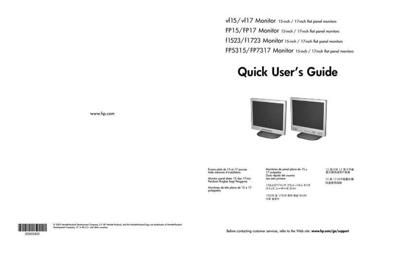
HP vf15 User manual

ServiceManual
15-inch LCD Monitor
vf15 / FP15 / f1523/ FP5315

Service Manual Versions and Revision
Copyright
Copyright 2003LiteOn Technology Corp.
All Rights Reserved
This manual maynot,in wholeorin part,be
copied, photocopied,reproduced, translated, or
convertedto any electronic ormachine readable
form without priorwrittenpermissionof LiteOn
TechnologyCorp.
vf15/FP15 /f1523 /FP5315 Service Manual.
Trademarks
LiteOn is a registered trademarkof LiteOn
Technology Corp.
All other trademarks are the property of their
respectiveowners.
No.VersionReleaseDateRevision
1.1.0Mar 17, 2003Originalrelease

Page1
vf15 /FP15/f1523/FP5315
1) Circuit
1.Power board operation therory----------------------------------------------------------------------------------------------3
2.Inverter--------------------------------------------------------------------------------------------------------------------------4
3.Power supply-------------------------------------------------------------------------------------------------------------------5
4.On-screen circuit---------------------------------------------------------------------------------------------------------------5
5.Video inputcircuit-------------------------------------------------------------------------------------------------------------5
6.Definition converter LSIperipheral circuit---------------------------------------------------------------------------------5
7.Systemreset,LED control circuit--------------------------------------------------------------------------------------------5
8.E
2
PROMforPNP---------------------------------------------------------------------------------------------------------------6
9.E
2
PROM-------------------------------------------------------------------------------------------------------------------------6
10.CPUcircuit----------------------------------------------------------------------------------------------------------------------6
10.1Dection of POWER switchstatus-------------------------------------------------------------------------------------6
10.2Displaymodeidentification--------------------------------------------------------------------------------------------6
10.3 Usercontrol---------------------------------------------------------------------------------------------------------------7
10.4 ControlofidentificationconverterLSI(IC306)----------------------------------------------------------------------8
10.5 PowerONsequence-----------------------------------------------------------------------------------------------------9
10.6 PowerOFFsequence--------------------------------------------------------------------------------------------------10
11.AudioCircuit-----------------------------------------------------------------------------------------------------------------11
2)Troubleshooting
1.Nodisplay of screen(Screenisblack,color of LED isamber)--------------------------------------------------------12
2.Nothing displayson screen(Screen is black, color ofLED is green)------------------------------------------------13
3.Checking the back lightunit-----------------------------------------------------------------------------------------------16
4.Abnormalscreen-------------------------------------------------------------------------------------------------------------17
5.NoOSD display--------------------------------------------------------------------------------------------------------------18
6.Abnormal plug and playoperation---------------------------------------------------------------------------------------19
7.Checking the interface circuit ofsync signal----------------------------------------------------------------------------20
7.1 Checkingthe control circuit ofhorizontal sync pulse-------------------------------------------------------------20
7.2 Checking the control circuitof vertical sync pulse----------------------------------------------------------------20

Page2
vf15 /FP15/f1523/FP5315
8.Checking the resolution change IC movement--------------------------------------------------------------------------21
9.Checking theDC/DC converter circuit-----------------------------------------------------------------------------------22
10.No power on------------------------------------------------------------------------------------------------------------------23
11.Checking thepanel circuit--------------------------------------------------------------------------------------------------24
12.Checking inverter board circuit--------------------------------------------------------------------------------------------25
3)RecommendedParts List
Recommended PartsList---------------------------------------------------------------------------------------------------26

Page3
vf15 /FP15/f1523/FP5315
1. Power Board Operation Therory
1.1LinefilterconsistsofC801,T801, C802, C803, C804,C837, C838. Iteliminates high frequencyinterference to meet
EMI srequirement.
1.2Rec &Filter
Bridgediode D801 convertsAC sourceintopulsed DC.Thispulsed DCissmoothedandfilteredby C805. R802
is anNTC ( negative thermal coefficient) resistor, used to reduceinrush current to be within safe range.
1.3Powertransformer:
T802 convertsenergyfor square wave frompower sourceC805 to secondaryside to generate+12Vand+15V.
1.4Output :
The squarewave fromT802 is rectifiedbyD809, D810, then filteredbyC817, C822 togenerate +15Vand+12V
respectively.
1.5Driver:
Q803 drive T802 fromPWM controlofI801 for power converted.
1.6FB:
Negativefeedback CKTconsists of photo coupler I802 and adjustable regulator I803. It can maintain output
voltages+15V and+12Vatastablelevel.
1.7PWM :
1.7.1Start: Whenpower is turned on.C807 is charged a 15 volt and a starting current above 40uA to pin7 of I801.
I801 starts to oscillate and outputs a pulse train through pin 6 to drive Q803.
1.7.2OPP: When Q803 turns on, C805 supplies a linearly increasing triangle currentthrough the primary inductance
of T802 to thedriver Q803, oncethepeakvalue of thiscurrent multiplied byR811 exceeds1volt, pulsetrain will
be turnoffimmediately to protectQ803, T802 frombeing burned out.
1.7.3Regulation: If outputvoltage+15V goes up, the Rterminal ofI803 gets more bias, accordingly photo transistor
and photo diode flows more current. The voltage of pin 2 goes up too, making the pulsewidth of pin 6 to
become narrower. So the output voltage +15Vwill be pulled down to a stable value.
1.7.4OVP:If+15Vgoes up too much, the induced voltageon pin 4 of T802 becomeslargealso. Supposethat it is
over 18 volts, ZD801 conducts, pin3 of I801 is pulled up over 1 volt.Thepulsetrainatpin 6 goesdownto zero,
shutting Q803 off immediately.
1.7.5SCP: If output terminal isshort to ground, photo transistor does not conduct, hence Q806 does not conduct
either. Thenoscillation of I801 is stop, shuttingQ803 off immediately.
Line
Filter Rec. &
Filter Power
Transformer Outpur Rec. & Filter
PWM Driver
FB
HPD-K15AA Power Board Block Diagram

Page4
vf15 /FP15/f1523/FP5315
2.Inverter
This unit operates on an output voltage of 15Vfrompower source.
2.1Regulator:Q101 get a+5VDC for I101 powersupply.
2.2UVP: Q106 turnsoffwhen theVinisunder 10V.Then pin3of I101 is pulledlow andinverteroff immediately.
That is the undervoltage protection.
2.3ControlIC:I101(OZ960S)
2.3.1Enable :When pin 3ofI101 is over1.5V,I101 works.Ifitis under1.5V,I101 turns off.
2.3.2OSC:WhenI101 enabled, R108/C115 (pin17/pin18 ofI101) determinethe operating frequency.
2.3.3SST: C104 (pin 4of I102) provides soft start function.
2.3.4Ignition: R109 (pin 8 of I101) provides higher operating frequencyfor more striking voltage until regulation of
feedback of lampcurrent. C103 (pin 1ofI101) determine the striking time.
2.3.5Dimming control:The divided voltage of R106/R105/R104 control the dutypulse of burst-mode to drive Q105
andperform awidedimming control for theCCFL. Theburst-mode frequency is determinedby C116.
2.3.6Regulation: Pin 9/pin 10 ofI101 provideregulationoftheCCFL current fromfeedback.The non-inverting reference
(pin10of I101)isat1.25V nominal.
2.3.7Protection:Open-lamp protection in the ignition period isprovided through bothpin1 and pin2 of I101.
Removalof the CCFLduringnormaloperation willtriggerQ107 toturnson andshutsofftheinverter.Thisislatch
function.
2.3.8Outputdrivers: Theconfiguration prevents anyshoot-through issue associated with bridge-type power
conversionapplications.Adjusting the overlapconduction between I102 P-MOSFET and I103N-MOSFET,
I102N-MOSFET andI103 P-MOSFET,the CCFLcurrentregulationis achieved.
2.4Full-bridgeswitching/Transformer:I102/I103/C123/I104/I105/C137/C125/T101/T102composefull-bridgeswitching
toconvertDCintoAC for drivertheCCFL.
2.5Detection: C124/C125/C126detect the output voltage and ensure a ratedvoltage bypin2 of I101.Q108/Q109
ensurenot a open-lamp.
2.6Feedback:D119/R123/D120 sense the lampcurrentfor negative feedbackand regulation.
Inverter Circuit
VCC
Regulator
U.V.P. Enable
OSC
SST
Dimming
control
Output driver
Protection
Ignition
Regulation
Control IC : OZ960
ON / OFF
Full-bridge switching Transformer Lamp
Feed back
Detection
Brightness
control
VDD

Page5
vf15 /FP15/f1523/FP5315
3.Powersupply(CircuitdiagramsMainPWB)
3.1Line filter consists ofFB326, FB327, FB328. It eliminateshighfrequency interferenceto meet EMI srequirement.
3.2I3093.3Vand2.5VDC-DCrequlator
A3.3Vand2.5VDC powersupplyfor LCDmodule andASIC.
3.3A9.2VDCpowersupply for LCDmodulesource ICisgenerated from I311.
3.4A6VDCpowersupply for LCDmoduleto controlgate IC OFF is generatedfromI311.
3.5A18VDC power supply for LCDmoduletocontrol gate ICON isgeneratedfromI311.
3.6A3.6VDC powersupply for LCDmodule to control panelGamut ofV-Com.
4.On-screen circuit(CircuitdiagramsMain PWB)
I303(gm2115)Embededfunction.
On-screen menuscreen is established and the resultant data are output fromI303 (Circuit diagramMAINPWB ,
gm2115).
5.Videoinputcircuit(CircuitdiagramMAINPWB)
The AC-coupled videosignalis used to clamp the black level at 0V).
6.DefinitionconverterLSIperipheralcircuit(CircuitdiagramMAINPWB)
I303 gm2115 is thedefinitionconverter LSI.
The analog R, G,Bsignal input enteredfromthe video input circuitis convertedinto the digital dataof video
signal through theincorporated A/D converter. Based onthisconversion,thisdevice performs interpolation
during pixelextension. The sourcevoltage for thisdeviceis 3.3V and 2.5Vthe system clockfrequencyis14.
318MHz.
Thewithstand voltage levelfor the input signal voltage is 3.3Vand 5V.
7.Systemreset,LEDcontrolcircuit(Circuit diagramMAIN PWB)
7.1System reset
Systemreset isperformed bydetecting the rising of the5V source voltageat I305.
7.2LEDcontrolcircuit
Green /amberis litwiththe controlsignal ofthe LEDGREENandLEDAMBERsignal pin49, 48fromI303(Circuit
diagramMAINPWB).

Page6
vf15 /FP15/f1523/FP5315
8. E2PROM for PnP (CircuitdiagramMAIN PWB 3/7)
Data transfer between I308 and host.
Therearetwo forms ofcommunications protocal.Inboth, displaycapabilities are retrievedbythesystemsoftware
during theboot-up and configuration time.
For the PCplatform,thissoftware layer isdefined in theVESABIOS Extension /DisplayData Channel,DDC2,
standard.
9. E2PROM (Circuit diagramMAIN PWB 4/7)
Datatransfer between I306(24LC16B) andI303(Circuit diagramMAINPWBpage 4/7 (I306)iseffectedthrough the
IIC busSCL(pin52) and SDA(pin 51) of I303. Thedatatobe transferred toeach devicearestored inI306.
l I303 control data.
l OSD related setting data.
l Other control data forservice menu.
10.CPU circuit(CircuitdiagramMAIN PWB4/7)
I303(gm2115) embeded microcontrollerwith parallelROM interface(I302).
Thesource voltagefor thedeviceis3.3V and2.5Vthesystem clockfrequency is14.318MHz.
10.1Detection of POWER switch status
TheI303 identifiesthe ONstatusof the twopower supplies. The identificationis made whenthe power supplyis
turned off. For example, if the power supplyis turned off with the POWER switch, the POWER switch must be
turned onwhenactivating the powersupplyagain.Ifthe powersupplyisturnedoff bypulling outthepower
cord, thenthis power supplycanbe turned onbyconnectingthepower cord, withoutpressingthe POWER
switch.
10.2Display modeidentification
10.2.1Functions
(1)Display modeidentification
l The displaymode of input signal is identified based on Table 1, and according tothe frequencyand polarity
(HPOL, VPOL) of horizontal or vertical sync signal, presence of theresolutionor vertical syncsignal, and the
discrimination signal (HSYNC_DETECT, VSYNC_DETECT).
l When the mode has been identified through the measurement of horizontal and vertical frequencies, thetotal
number of lines is determined with a formula of “Horizontalfrequency/ Vertical frequency= Totalnumber
of lines. “Finalidentificationcanbe madebyexaminingthecoincidenceoftheobtained figure withthe
numberof lines for the mode identifiedfromthe frequency.
l When the detected frequencyif the sync signal has changed, the total number of linesshould be counted even
through it isregistor identified frequencyinthesamemode. Then,it isnecessaryto examinewhether the
preset value for the vertical displayposition has exceeded the total number of lines. If exceeded, a maximum
value should be set up, which does not exceed the vertical display position.
(2) Out-of-range
This out-of-range mode isassumed when the frequencyof the vertical signalis as specifiedbelow.
l Vertical frequencyequal to 85Hz into fail save mode.
l Vertical frequencyover 85Hz into out of range.
(3) Power save mode
Thepower save mode isassumed when the horizontal / vertical signals are as specified below.
l If there is no horizontalsync signal input.
l If there is no vertical sync signal input.

Page7
vf15 /FP15/f1523/FP5315
10.3User Control
1.Select MENU: To enter OSD menu.
2. (Down): To decrease the value of the parameter in the OSD, which has been selected for adjustment.
(Down): Choose the next OSD ICON.
3. ▲(Up): To increase the value of the parameter in the OSD, which has been selected for adjustment.
▲(Up): Choose the previous OSD ICON.
l If the horizontal sync signal is outside the measuring range of gm2115.
l If the vertical sync signal is outside the measuring range of gm2115.
Table 1
PolarityMode
No Resolution H-freq
(KHz)
Band Width
(MHz) HV
1. 102 VGA720 x 400 70Hz 31.47
28.322 -+
2. 103 VGA640 x 480 60Hz 31.47
25.175 --
3. 173 VESA640 X 480 72Hz37.86
31.5 --
4. 109 VESA640 X 480 75Hz37.5 31.5 --
5. 116 VESA800 x 600 60Hz37.88
40 ++
6. 110 VESA800 x 600 75Hz46.88
49.5 ++
7. 117 VESA800 x 600 72Hz48.08
50 ++
8. 108 MAC 832 x 624 75Hz 49.72
57.283 --
9. 118 VESA1024 x 768 60Hz48.36
65 --
10. 157 VESA1024 x 768 70Hz 56.48
75 --
11. 141 VESA1024 x 768 75Hz60.02
78.75 ++

Page8
vf15 /FP15/f1523/FP5315
10.3.1Relatedportsof I303
10.3.2Functions
Control is effected for thepush-switchesto be used when the user changes the parameters, in order to modifythe
respective setting values.Whether the switchhasbeenpressedisidentifiedwith theswitch inputlevel that is
turned “L”.
Each switch input port is pulled up at outside of I303.
Each parameter is stored in the EEPROM,the contents of which areupdatedas required.
10.4Controlofdefinitionconvertergm2115 (I303).
10.4.1Ports related to control
10.4.2Functions
Major function of I303 are as follows:
(1)Expansion of the displayscreen.
(2)Timing control for various signal types.
(3)Power-supplysequence (LCD panel).
Port
Pin No.
I/O
Signal name
FunctionRemarks
GPIO2147IPower
Power Switch Key
GPIO343IMANUALMenu Switch inputMENU key
GPIO747IDown-switch input
Down / AUTO key
GPIO646IUp+switch inputUp / BRI key
Pin No.
I/O
Signal name
Function
51I/OSDAGm2115 serial data
52OSCLGm2115 serial clock
207I/OHDATA2Gm2115 Address input
208I/OHDATA1Gm2115 Address input

Page9
vf15 /FP15/f1523/FP5315
10.5Power ONsequence

Page 10
vf15 /FP15/f1523/FP5315
10.6Power OFF sequence

Page 11
vf15 /FP15/f1523/FP5315
11.Audiocircuit(CircuitdiagramsMainPWB)
11.1Audioinput
The audio signal input received from the audio input terminal (P302) is applied tothe amplifier I301 of 1 and 9
through thelow-passfilter consisting of R305, R306, C314 andC315.
In thisamplifier,controlsofVolumeareavailavle. The audiosignal controlled at theVR601 determines the attenu-
ation of output of the amplifiers. Since then, the signal is output to the jack P303.
11.2Audio output
Theaudio signalis output fromthe jack output terminal (P303) of the jack board to the internalspeaker system.

Page 12
vf15 /FP15/f1523/FP5315
1.Nodisplay of screen (Screen isblack,colorofLEDis amber)
Does OSD display when
you push key button.
Yes
Check if the sync signal from Computer
is output and if the video cable is
connected normally.
No Proceed "No OSD display"section.
OK
Proceed "Checking the resolution change
IC movement" section.
NG Input the sync signal of computer, or
change the cable.
When a signal isn't
being inputted, it is
indicated with "NO
SIGNAL INPUT" or it is
indicated with "OUT OF
RANGE" at the time of
the frequency that it
can't be distinguished.

Page 13
vf15 /FP15/f1523/FP5315
2.Nothing displays on screen (Screen is black,colorof LEDis green)
Is backlight lit?
OK
Does computer output RGB video signals?
NG Refer "Checking the backlight unit" section
OK
Check OSD menu is displayed on screen
when you push the "MENU" key.
NG
1) Change pattern of video signal output on the
host.
2) Reconnect the video cable.
3) Change the video cable.
Check the video cable for failure. Check the host for
output signal with all black only.
OK NG
Proceed "Abnormal screen" section.
Next Page

Page 14
vf15 /FP15/f1523/FP5315
Continue
Check if the voltageon I309pin1 that
is highlevel DC at 5V.
Check the 3.3 V power are suppliedon I309 pin 4
and 2.5V onpin 5.
OK
NG
OK NG
Failure point
I309 Failure
Is a dot clock beingoutputted under the
condition that a LCD module is connected to
P308pin 3?
OK NG
Failure point
1) I303failure
2) Printed wirebroke betweenI303 andP308pin3.
Check the pulse of POL / HMS2/ HMS1 / LP /
STH are output on P308 pin 44, 45, 46, 47,
48 at TTL level.
OK NG
Failure point
1) I303failure
2) Printed wirebroke betweenI303 andP308pin44,
45, 46, 47, 48.
Check the CLKV/STV1pulse are output on
P307 pin 7, 8.
OK NG
Next Page
Failure point
1) I302failure
2) Printed wirebroke betweenI303 andP307pin7, 8.
Failurepoint
1) Printed wirebroke between P309 and I309.
2) FB327, FB328 or FB331 open.
1) Check +18V / +3.6V / -6V on P307 and +3.3V.
2) Check +9.2 V onP308.
OK
NG Refer "Checking the panel power circuit"

Page 15
vf15 /FP15/f1523/FP5315
Continue
Check the data signal output on P307 and
P308 R, G, B data pin.
OK NG
Failure point
1) I303 failure.
2) Printed wire broke between I303 and P307 , P308
data line.
Failure point
1) The cable broke between P307 , P308
and LCD module.
2) LCD module failure.

Page 16
vf15 /FP15/f1523/FP5315
3. Checkingtheback lightunit
Is+12Vsupplied to CN101
pin 1, 2 to inverter PWB?
OK NG Failure point
Inverter cable disconnection.
Checkthe INV_EN signal input to Inverter Board Q104 at TTL high level.
OK
NG Isa "H"level being output in the TTL level from I303 pin 114
Or, isINV_EN signal being output?
NG
Failure point
Printed wire broke between I303 pin 114
and Inverter Board Q104.
Check the PWM signal of the input from I303 pin 40 is a BRI signal
OK NG Failure point
1)Printed wire broke between
I303 pin 40 and Q313, Q312.
2)I303 failure
Failure point
1) Inverter of LCD module failure.

Page 17
vf15 /FP15/f1523/FP5315
OK NG
Failure point
1)No R, G andB video signal output from host computer. Check
computer
2)Videosignal cabledisconnection.
OK NG
Check the R, G, B videosignal from computer input on
D-Sub R, G, B connector.
Check the R, G, B input signals onI303
pin 171, 167, 163respectively that theirlevel is 0.7Vp-p
maximum.
Is the pulse of the TTLlevel being output to P307, P308
from the data line of I303?
Failure point
In case of theRedsignal. (A Green and Bluesignal is the same
path, too.)
1)Printedwirebroke between D-Sub(R)and I302pin 171.
2)R334short.
3)C339open.
4)R332open.
OK NG Failure point
1)Printedwirebroke between I303 dataline and P307, P308
2)I303failure.
Check pulse of POL/HMS2/HMS1/LP/STH are output to
P308 pin 44, 45, 46, 47, 48 at TTL level.
OK NG
Failure point
1)Printedwirebroke between I303 and P308 of control line.
2)LZ301~LZ312 open orRP303~RP314 open.
3)CN301~CN312 short
Check the pulse of CLKV/STV1are output toP307
pin7, 8.
OK NG
Check the CLKH OUTPUT to P308 pin3 from I303 pin
115 at TTL level.
OK NG
Process "Checking the resolutionchange ICmovement"
section.
Failure point
1)Printedwirebroke between I303 pin115andP308 pin3.
2)FB324 open
3)FB325 open
4)C401short
Failure point
1)Printedwirebroke between I303 and P307 of control line.
2)R357, R355 open
3)C394, C393 short
4.Abnormalscreen

Page 18
vf15 /FP15/f1523/FP5315
5.NOOSDdisplay
OK
NG
Confirm the MENU key is pressed at that moment.
Proceed "Checking the resolution change IC movement" section.
Failure point
1) Function key is destroyed.
2) FB305 open.
3) RP302 open.
4) I303 failure.
Other manuals for vf15
2
This manual suits for next models
3
Table of contents
Other HP Monitor manuals

HP
HP OMEN 32c Manual

HP
HP L2401x User manual

HP
HP MX703 - Pavilion - 17" CRT Display User manual

HP
HP VH240a User manual

HP
HP V24 Manual

HP
HP L1940T Installation guide

HP
HP L2035 User instructions

HP
HP 1332A Service manual

HP
HP Engage 14 Assembly instructions

HP
HP TS 23W8H - 23" De-Branded Widescreen LCD Full HD 1080p... How to use