Icom IC-A200 User manual

VHF AIR BAND TRANSCEIVER
iC-a200
S-14227MZ-C1
Apr. 2006

This service manual describes the latest service information
for the following transceivers at the time of publication.
Be sure to include the following four points when ordering
replacement parts:
1. 10-digit order numbers
2. Component part number and name
3. Equipment model name and unit name
4. Quantity required
<SAMPLE ORDER>
1120002170 IC M5223FP IC-A200 MAIN UNIT 5 pieces
8810006840 Screw FH M2.6×4 IC-A200 Top cover 10 pieces
Addresses are provided on the inside back cover for your
convenience.
NEVER connect the transceiver to an AC outlet or to a DC
power supply that uses more than 16 V. This will ruin the
transceiver.
DO NOT expose the transceiver to rain, snow or any liquids.
DO NOT reverse the polarities of the power supply when
connecting the transceiver.
DO NOT apply an RF signal of more than 20 dBm (100 mW)
to the antenna connector. This could damage the trans-
ceiver's front end.
Icom, Icom Inc. and logo are registered trademarks of Icom Incorporated (Japan) in the United States, the United
Kingdom, Germany, France, Spain, Russia and/or other countries.
INTRODUCTION CAUTION
ORDERING PARTS
MODEL VERSION NO. VERSION SYMBOL
IC-A200 #01 U.S.A. USA
IC-A200F #02 France FRA
IC-A200
#03 United Kingdom UK
#04 Germany FRG
#05 Australia AUS
1. Make sure a problem is internal before disassembling
the transceiver.
2. DO NOT open the transceiver until the transceiver is
disconnected from its power source.
3. DO NOT force any of the variable components. Turn
them slowly and smoothly.
4. DO NOT short any circuits or electronic parts. An
insulated turning tool MUST be used for all adjustments.
5. DO NOT keep power ON for a long time when the
transceiver is defective.
6. DO NOT transmit power into a signal generator or a
sweep generator.
7. ALWAYS connect a 40 dB or50 dB attenuator between
the transceiver and a deviation meter or spectrum
analyzer when using such test equipment.
8. READ the instructions of test equipment thoroughly
before connecting equipment to the transceiver.
REPAIR NOTES

TABLE OF CONTENTS
SECTION 1 SPECIFICATIONS
SECTION 2 INSIDE VIEWS
SECTION 3 CIRCUIT DESCRIPTION
3 - 1 RECEIVER CIRCUITS .................................................................................................... 3 - 1
3 - 2 TRANSMITTER CIRCUITS ............................................................................................. 3 - 3
3 - 3 PLL CIRCUITS ................................................................................................................ 3 - 4
3 - 4 VOLTAGE LINES ............................................................................................................. 3 - 5
3 - 5 CPU PORT ALLOCATIONS ............................................................................................ 3 - 5
SECTION 4 MEMORY PROTECTION
4 - 1 MEMORY PROTECTION PROGRAMMING ................................................................... 4 - 1
4 - 2 MEMORY PROTECTION CANCELLING ........................................................................ 4 - 1
SECTION 5 CONNECTIONS
5 - 1 WIRING CONNECTION .................................................................................................. 5 - 1
5 - 2 MOLEX CONNECTOR .................................................................................................... 5 - 2
5 - 3 RACK MOUNT ASSEMBLY ............................................................................................. 5 - 3
SECTION 6 ADJUSTMENT PROCEDURES
6 - 1 PREPARATION BEFORE SERVICING ........................................................................... 6 - 1
6 - 2 PLL ADJUSTMENT ......................................................................................................... 6 - 2
6 - 3 RECEIVER ADJUSTMENT ............................................................................................. 6 - 2
6 - 4 TRANSMITTER ADJUSTMENT ...................................................................................... 6 - 4
SECTION 7 MECHANICAL PARTS AND DISASSEMBLY
SECTION 8 PARTS LIST
SECTION 9 BOARD LAYOUTS
9 - 1 MAIN UNIT ...................................................................................................................... 9 - 1
9 - 2 FRONT UNIT ................................................................................................................... 9 - 3
9 - 3 PA UNIT ........................................................................................................................... 9 - 3
9 - 4 PLL UNIT ......................................................................................................................... 9 - 5
9 - 5 VCO UNIT ........................................................................................................................ 9 - 5
9 - 6 DIAL UNIT ....................................................................................................................... 9 - 5
SECTION 10 BLOCK DIAGRAM
SECTION 11 VOLTAGE DIAGRAM

1 - 1
SECTION 1 SPECIFICATIONS
GENERAL
• Frequency range : 118.000–136.975 MHz
• Mode : AM (6K00A3E)
• Tuning steps : 25 kHz, 50 kHz or 1 MHz
• Number of memory channels : 9
• Frequency stability : ±0.0015% (–20°C to +55°C)
• Antenna impedance : 50 Ω
• Power supply requirement : 13.75 V DC ±15% (negative ground)
• Current drain (at 13.8 V DC) :
• Usable temperature range : –20°C to +55°C; –4°F to +131°F
• Dimensions : 160 (W)×34 (H)×271 (D) mm; 6.3 (W)×1.3 (H)×10.7 (D) in
(Projections not included)
• Weight (approx.) : 1.1 kg; 2.4 lb
TRANSMITTER
• Output power (at 13.8 V DC) : 7 W (Carrier power)
• Modulation : 70% (Max 98%)
• Microphone impedance : 600 Ω
• Modulation system : Low level modulation
• Spurious emissions : Less than –60 dB
RECEIVER
• Receive system : Double-conversion superheterodyne
• Sensitivity : 2 µV for 6 dB S/N (with 1 kHz, 30% modulation)
• Spurious rejection : 70 dB
• Selectivity : ±8 kHz/6 dB (min.)
±17 kHz/40 dB
±22 kHz/60 dB
• Intermediate frequencies : 1st 32.455 MHz
2nd 455 kHz
• Audio output power : 5 W with a 4 Ω load
60 mW with a 500 Ω load
Transmit 2.6 A
Receive Max. audio output 600 mA
Squelched 320 mA

SECTION 2 INSIDE VIEWS
2 - 1

3 - 1
SECTION 3 CIRCUIT DESCRIPTION
3-1 RECEIVER CIRCUITS
3-1-1 ANTENNA SWITCHING CIRCUIT (PA UNIT)
The antenna switching circuit functions as a low-pass filter
while transmitting and as a resonator circuit while receiving.
Received signals enter the PA unit from the antenna
connector and pass through the low-pass filter (C54–C57,
C66, L14–L16), the antenna switching circuit (D7–D9) and
the bandpass filter (C71–C75, L21–L23). The signals are
then applied to the MAIN unit.
3-1-2 RF CIRCUIT (MAIN UNIT)
The RF circuit amplifies signal within the range of frequency
coverage and filters out-of-band signal.
The signals from the PA unit pass through the attenuator
circuit (D6, D7). The attenuation level is controlled by AGC
voltages. The signals are passed through a bandpass
filter and are then amplified at the RF amplifier (Q1). The
amplified signals are passed through a bandpass filter again
and are then applied to the 1st mixer circuit (Q4).
The bandpass filters employ tuned-type filters using varactor
diodes (D1–D4) with PLL lock voltages to suppress the out-
of-band signals (especially FM broad band signals) and to
obtain high image response rejection.
AGC voltage is applied to Q1 as the bias voltage to obtain
wide range characteristics of signal strength.
3-1-3 1st MIXER AND 1st IF CIRCUITS (MAIN UNIT)
The 1st mixer circuit converts the received signals to a fixed
frequency of the 1st IF signal using a PLL output frequency.
By changing the PLL frequency, only the desired frequency
will be passed through a crystal filter located at the next
stage of the 1st mixer.
The signals from the bandpass filter are mixed with a 1st
LO signals from D25 at the 1st mixer (Q4) to produce a
32.455 MHz 1st IF signal. The 1st IF signal passes through
the crystal filter (FI1) and is then applied to the IF amplifier
(Q6).
3-1-4 2nd MIXER AND 2nd IF CIRCUITS
(MAIN UNIT)
The 2nd mixer circuit converts the 1st IF signal to a 455 kHz
2nd IF signal. A double superheterodyne system (which
converts the received signal twice) improves the image
rejection ratio and obtains stable receiver gain.
The 1st IF signal from the 1st IF amplifier (Q6), is applied
to the 2nd mixer (IC14) and mixed with a 32.000 MHz
2nd LO signal from Q20 to be converted to a 455 kHz of
signals. The 2nd LO signal is commonly used with the PLL
reference oscillator.
The 2nd IF signal is applied to an IF filter (F12) to suppress
out-of-band signals. The 2nd IF signal is amplified at the IF
amplifiers (Q7–Q10) and is then applied to the AM detector
circuit (Q49).
The thermistor (R33) is used for Q9 bias voltage to obtain
stable amplifier gain during temperature fluctuations.
RECEIVER CIRCUIT BLOCK DIAGRAM

3 - 2
3-1-5 AM DETECTOR CIRCUIT (MAIN UNIT)
The AM detector circuit demodulates the 2nd IF signal to
AF signals.
The 2nd IF signal from Q10 is detected at the AM
detector (Q49) for conversion to AF signals. A PN junction
construction inside Q49 is used for AM detection to obtain
low output impedance. High frequency components are
removed by capacitors (C239, C241, C242) and passed AF
signals are applied to the AF circuits.
3-1-6 AF CIRCUIT (MAIN UNIT)
The AF signals are passed through the active low-pass
filter (Q13) and are amplified at the limiter amplifier (IC16,
pin 2). The amplified signals from IC16 (pin 3) pass through
the volume control (R89) on the front panel and are then
applied to the AF preamplifier (IC17, pin 3).
The limiter amplifier (IC16) has an ALC limiter circuit that
maintains the audio level even when receiving shallow or
deeply modulated signals. The AF signal level is detected at
D40 and is fed back to IC16 (pin 4) to control the amplifier
gain.
The amplified signals from the AF preamplifier (IC17) are
passed though the active low-pass filter (Q39) and the
speaker switch (Q38) and are then applied to the AF power
amplifier (IC5). IC5 amplifies the signals to a level needed
to drive a 4 Ω external speaker.
3-1-7 SQUELCH CIRCUIT (MAIN UNIT)
The squelch circuit cuts out AF signals when receiving no
modulated signal. When no voice modulation is included
in the signal, the squelch circuit cuts out the AF signal by
comparing voice audio and noise audio components in the
AF detected signals.
The AF detected signals from Q49 are separately applied
to the active low-pass filter (IC3b) and active high-pass filter
(IC3a) to amplify voice components (lower than approx.
3 kHz) and noise components (higher than approx. 4 kHz)
respectively. Both outputs are applied to the comparator
(IC4a). When noise components are larger than audio
components, the comparator outputs "HIGH" to turn Q14
ON. Hence Q14 grounds the audio detected line and the AF
signal is cut out.
3-1-8 AGC CIRCUIT (MAIN UNIT)
The AGC (Automatic Gain Control) circuit reduces RF and
IF amplifier gain and activates the RF attenuator (D6, D7)
by decreasing the bias voltage to prevent distortion from
strong signals.
The signal from the 2nd IF amplifier (Q10) is detected at D8,
and applied to the base of Q50. When receiving a strong
signal, Q50 is turned ON to decrease the bias voltage.
Minus voltages are applied to the emitter of Q50 to operate
the AGC at low signal levels. The PLL reference oscillation
frequency (32.00 MHz) is rectified by the detector (D20,
D21, C116, C117) to obtain minus voltages (–4.5 V approx.).
The AGC release time is determined by C49 and R310. Q51
activates for strong signals.
SQUELCH CIRCUIT

3-2 TRANSMITTER CIRCUITS
3-2-1 MIC AMPLIFIER CIRCUIT (MAIN UNIT)
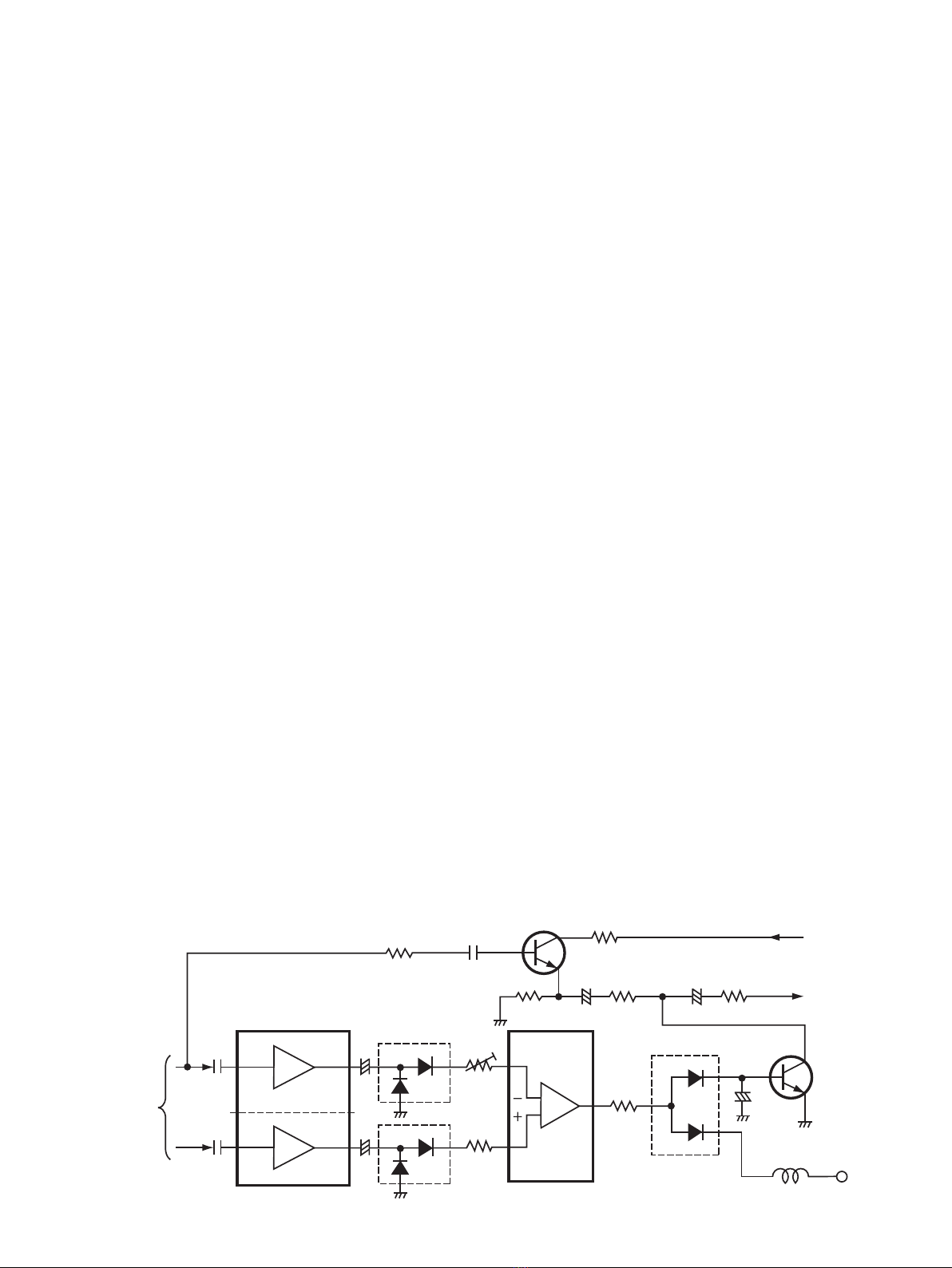
The mic amplifier circuit amplifies the mic audio with the
limiter circuit to a level needed for the AM modulator.
Mic audio signals pass through the mic switch (Q4) and are
then applied to the limiter amplifier (IC13, pin 2). The mic
switch cuts out the mic audio signal while receiving.
IC13 has an ALC limiter circuit that controls the amplifier
gain to prevent signal distortion. A portion of the output
signals from IC13 (pin 3) is detected by D18 and its
detected voltages feed back to IC13 (pin 4) to control the
gain.
The output signals from IC13 (pin 3) pass through the active
low-pass filter (Q47) to cut out components higher than 2.5 kHz
and are then amplified at the mic amplifier (Q40). The signals
are then applied to the AM modulator (Q36, Q31).
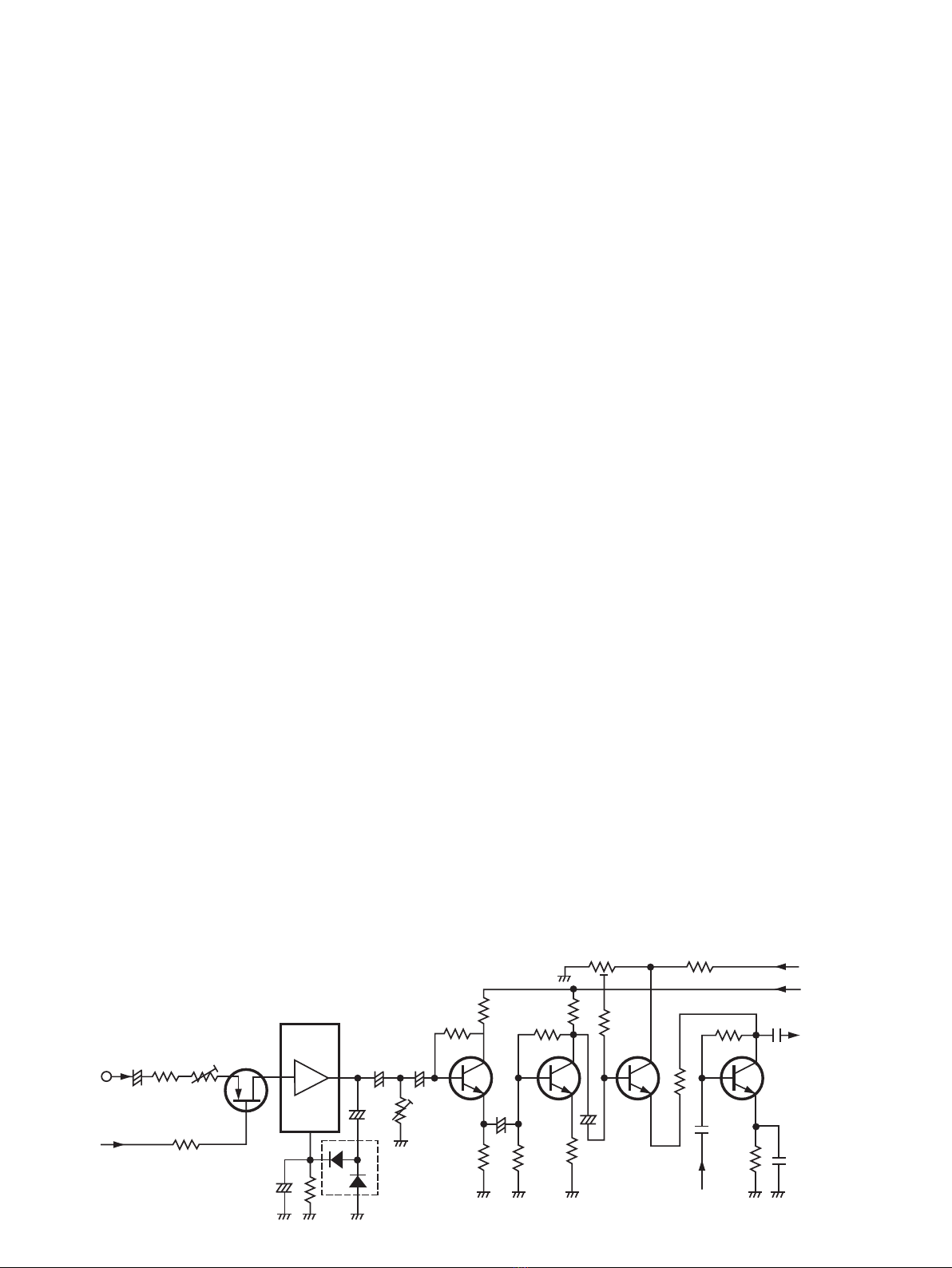
3-2-2 MODULATOR CIRCUIT (MAIN UNIT)
The modulator circuit controls the collector voltage of the
transmitter linear amplifier to obtain amplitude modulation.
The modulator circuit consists of a current amplifier and a
linear amplifier. Amplified audio signals are applied to the
current amplifier (Q36) which controls the collector voltage
of the linear amplifier (Q31). The LO signal is amplified at
Q31 with variable voltage related to the mic input level so
that the LO signal level is varied as an AM modulation.
3-2-3 LOCAL SIGNAL AMPLIFIER CIRCUIT
(MAIN UNIT)
The LO signal (118.00–136.975 MHz) is obtained by mixing
the PLL output frequency (150.00–168.975 MHz) and
reference oscillator signal (32.00 MHz).
The PLL output and the reference oscillator signals are
amplified at Q29 and Q20 respectively and are then applied
to the transmitter mixer circuit (IC15). The mixed signal
is passed through the transmitter bandpass filter to re
move the out-of-band signals. Q30 is a buffer amplifier to
compensate for bandpass filter attenuation.
The passed signal is modulated at Q31 and amplified at
Q44. The attenuator-type ALC control circuit (D33, D34,
R356) reduces the signal level when a mismatched load
occurs.
3-2-4 DRIVE AND POWER AMPLIFIERS (PA UNIT)
The signal from the MAIN unit is amplified at 3 amplifiers,
the pre-driver (Q5001), the driver (Q5003) and the final
amplifier (Q5005) in the PA unit to obtain the stable 7 W
output power.
The amplified signal passes thorough the matching circuit
(C34, C35, C59–C61), the ALC detector circuit (L13, D3–
D6), the antenna switching circuit (D7), and the low-pass
filter (L14–L16, C54–C57, C66). The signal is then applied
to the antenna connector.
3-2-5 ALC CIRCUIT (MAIN AND PA UNITS)
The RF ALC circuit protects the final amplifier (Q5005) from
a mismatched output load.
A portion of the output power from the final amplifier
(Q5005) is detected at the ALC detector (D5003–D5005)
on the PA unit. This detected voltage is set at a minimum
value when the output load is correct. However, when
mismatching occurs the detected voltage is increased.
The detected voltage is applied to the MAIN unit as an ALC
signal. The comparator (IC18) in the MAIN unit compares
the difference between the detected voltage (pin 5) and
reference voltage (pin 6). The comparator outputs "HIGH"
when mismatching occurs. The output current flows through
the attenuator-type ALC circuit (D33, D34, R356) to change
the attenuation ratio and to decrease the RF signal level.
MIC AMP AND MODULATOR CIRCUITS
3 - 3

3-3 PLL CIRCUITS
3-3-1 GENERAL (PLL UNIT)
The PLL circuit steadily oscillates the transmit and receive
local frequencies while comparing the phase of the divided
VCO frequency and reference frequency. Therefore, the PLL
output frequency is controlled by the divided ratio (N-data)
of the programmable divider.
The oscillated signal in the VCO circuit is divided by N-data
at a programmable, divider and is phase detected with the
reference frequency at a phase comparator. The detected
signal (pulse-type signal) is rectified by a loop filter and
converted to DC voltage (PLL lock voltage). This voltage is
applied to varactor diodes in .the VCO unit to control the
oscillating frequency. Hence, this loop provides a variable
and stable oscillating frequency.
IC2001 includes the prescaler, programmable divider, phase
comparator, etc. in one chip.
3-3-2 REFERENCE OSCILLATOR CIRCUIT
(MAIN UNIT)
The reference frequency oscillator oscillates at a stable
32.000 MHz which is used for the PLL reference frequency,
receive and transmit LO frequency. AGC minus voltages are
used to detect this frequency.
The reference frequency (32.000 MHz) is generated by the
oscillator circuit of IC19 and X1. The reference frequency
is divided by 4 at IC1 and is then applied to the PLL board.
The frequency is divided again in PLL IC (IC2001) by 1/320
to obtain the PLL reference frequency of 25 kHz.
3-3-3 VCO CIRCUIT (VCO UNIT)
The VCO circuits oscillate the PLL output frequency by
controlling varactor diodes (D2001–D2003).
The VCO circuits (Q2004) employs a clap oscillator circuit.
The signal generated at the VCO is buffer-amplified at
Q2001 or Q2002. The amplified signals are used for a
receive/transmit LO signal as PLL output (OUT2) or used
for a feedback signal (OUT1) to the PLL circuit.
3-3-4 PHASE DETECTOR CIRCUITS (PLL UNIT)
The phase-detector circuit detects the out-of-phase
components of the VCO frequency using a stable reference
frequency.
The PLL IC (IC1001) contains a prescaler, programmable
divider, high-speed phase detector and shift register. The
oscillated signal comes from the VCO board and enters
IC1001 (pin 11). Then, it is divided at the prescaler and
divided again at the programmable divider. The divided
signal is applied to a phase detector to compare it with a
reference frequency (25 kHz). The detected signal exits
IC1001 (pin 7).
3-3-5 LOOP FILTER CIRCUIT
An active loop filter circuit is adopted for this PLL circuit to
convert the phase-detected signal to DC voltage (PLL lock
voltage) and to obtain needed levels to control the VCO
circuit.
The active loop filter (Q1002–Q1004) converts the phase-
detected signal (pulse-type signal) to DC voltage (PLL lock
voltage) to control the VCO oscillating signal. The PLL lock
voltage changes the reactance of varactor diodes in the
VCO circuit.
PLL VCO CIRCUIT
3 - 4

3-4VOLTAGE LINES 3-5 CPU PORT ALLOCATIONS
LINE DESCRIPTION
Vcc A voltage line from the external DC power
connector.
T8V
Used for the transmitter circuit.
Produced by the T8V regulator (Q34, Q35, D32)
and controlled by the T/R switching circuit
(IC10a–IC10c).
R8V Used for the receiver circuit.
Produced by the R8V regulator (Q32, Q33, D30).
8V A common 8 V line from the 8V regulator (IC11).
5V A common 5 V line from the 5V regulator (IC12).
–4.5V
Used for the AGC circuit.
Produced at D20, D21 by detecting the reference
oscillation signal.
Pin No. Port No. Description
1 P72 Input port for the frequency exchange
switch.
2 P71 Input port for the channel switch.
3 P70 Input port for tuning step selection
LOW: 25 kHz HIGH: 50 kHz
4, 5 P63, P62 Input ports for the large tuning control.
P63: MHz down P62: MHz up
6, 7 P61, P60 Input ports for the small tuning control.
P61: kHz down P60: kHz up
15 P41 Outputs the protect register enable
signal.
16 P40 Outputs the program enable signal.
20 RESET When receiving the reset signal "HIGH"
to "LOW", the CPU starts its operation.
21 X1 Oscillator input port for the CPU clock
frequency.
22 X2 Oscillator output port connected in
parallel with the X1 port.
23 P33 Outputs the chip select signal to IC8.
24 P32 Outputs the serial clock to IC8.
25 P31 Serial data output to IC8.
26 P30 Serial data input from IC8.
27 P81 Input port for a remote exchange switch.
28 P80 Input port for a remote channel switch.
30 SO Outputs PLL serial data.
31 SCK Outputs serial clock to the PLL.
40 P23 Outputs beep tones.
41 P22 Outputs a PLL strobe signal.
42 P21 Outputs the chip enable signal to an
LCD driver.
43 P20 Outputs an inhibit signal to an LCD
driver.
44 P73 Input port for PTT control.
3 - 5

SECTION 4 MEMORY PROTECTION
To prevent accidental changes, required memory channels
can be specified as protect channels. The contents of
protect channels CANNOT be changed by a user.
4-1 MEMORY PROTECTION PROGRAMMING
NOTE: DO NOT push and hold [ ] in steps 4), 7) and
9), or other functions are activated.
1) Before setting or cancelling, extract the transceiver from
the mounting rack and open the top cover. Then connect
appropriate connector to the transceiver for operation.
2) Push and hold [CH] until the memory channel number
blinks.
3) Rotate the large or small tuning knob to select a memory
channel to be programmed as a protect channel.
4) Push [ ].
• Frequency content or “ − − − − ” blinks.
5) Rotate the large and small tuning knobs to select a
desired frequency.
6) Ground the memory protection pin (J7 on the MAIN
UNIT).
7) Push [ ].
8) Unground the memory protection pin.
• The memory channel is now programmed as a protect
channel.
9) Confirm that the frequency content DOES NOT blink
even when [ ] is pushed.
4-2 MEMORY PROTECTION CANCELLING
NOTE: DO NOT push and hold [ ] in steps 4), 6) and
7), or other functions are activated.
1) Push and hold [CH] until the memory channel number
blinks.
2) Rotate the large or small tuning knob to select a protect
channel to be cancelled.
3) Ground the memory protection pin as shown in the
diagram at left below.
4) Push [ ].
• Frequency content blinks.
5) Unground the memory protection pin.
6) Push [ ].
• The memory protection is now cancelled.
7) Confirm that the frequency content blinks when [ ]
is pushed.
4 - 1

SECTION 5 CONNECTIONS
5-1 WIRING CONNECTION
�
�
5 - 1

AUDIO WIRING
Use #24 AWG wires for connectors.
MEMORY CHANNEL AND FREQUENCY
EXCHANGE SWITCHES
For the memory channel switch and frequency exchange
switch, use a 2-position rocker switch or 2 separate
momentary push switches.
POWER CABLE WIRING
Use 2 pairs of #18 AWG wires for power and power
grounding wiring.
• Circuit breaker
To prevent physical damage, a 10 A circuit breaker MUST
be installed in the aircraft. Mount the circuit breaker in the
aircraft breaker panel or instrument panel to ensure easy
access during flight.
• Ground
The transceiver power ground is the airframe ground.
• jumpers
Pins 11, M, P, 13 MUST be jumped together with AWG
#20 wires or thicker.
TRANSMIT/RECEIVE INTERLOCK WIRING
When 2 transceivers are installed and both communication
antennas are top mounted, pin N MUST be connected to
pin 9 of each another transceiver.
INTERNAL FUSE
The IC-A200 has a 5 A internal fuse. If the power does not
turn ON, open the top cover and check the fuse.
DIMMER SELECTION
Connect pin B to the Instrument panel lighting line.
When the instrument panel lighting switch is placed to
dimmer position, the transceiver backlighting is reduced to
half brightness.
5-2 MOLEX CONNECTOR
ANo connection 1Ground for pin B
B+14 V lighting (input) 2Detected audio (output)
CAuxiliary audio 2 (input) 3Auxiliary audio 3 (input)
DAuxiliary audio 1 (input) 4Ground for pins D, C, 3
E4 Ω audio (output) 5Ground for pin E
FPower ground 6Power ground
H500 Ω audio (output) 7Ground for pin H
JComm microphone (input) 8Ground for pins J, K, 9
KIntercom microphone (input) 9PTT*
LMemory channel switch* 10 Squelch cancel*
M+ 13.8 V power (input) 11 +13.8 V power (input)
NTransmit/receive interlock 12 Frequency exchange switch*
PSwitched aircraft power (output) 13 Switched aircraft power (output)
RAircraft (input) 14 Aircraft power (input)
SPower ground 15 Power ground
*Ground to activate.
5 - 2

5-3 RACK MOUNT ASSEMBLY
5 - 3

SECTION 6 ADJUSTMENT PROCEDURES
6-1 PREPARATION BEFORE SERVICING
REQUIRED TEST EQUIPMENTS
EQUIPMENT GRADE AND RANGE
DC power supply Output voltage : 13.2 V DC
Current capacity : 2 A or more
RF power meter
Measuring range : 1–10W
Frequency range : 100–180 MHz
Impedance : 500
SWR : Less than 1.2:1
Frequency
counter
Frequency range : 0.1–180 MHz
Frequency accuracy : ±1 ppm or better
Sensitivity : 100 mV or better
Standard signal
generator (SSG)
Frequency range : 0.1–180 MHz
Output Level : 0.1 µV–32 mV
(−127 to −17 dBm)
Distortion meter Frequency range : 1 kHz ±10 Hz
Measuring range : 1–20%
EQUIPMENT GRADE AND RANGE
Oscilloscope Frequency range : DC–20 MHz
DC voltmeter Input impedance : 50 kΩ/DC or better
AC millivoltmeter Measuring range : 10 mV to 10 V
External speaker Impedance : 8 Ω
Ammeter Measuring range : 200 mA
Audio generator
(AG)
Frequency range : 200–2000 Hz
Output level : 1–200 mV
Attenuator Power attenuation : 40 or 50 dB
Capacity : 10 W or more
Modulation
analyzer
Frequency minimum : 180 MHz
Measuring range : 0–100%
CW: clockwise CCW: counterclockwise CP: check point
CONNECTION
6 - 1

6-2 PLL ADJUSTMENT
6-3 RECEIVER ADJUSTMENT
ADJUSTMENT ADJUSTMENT CONDITIONS
MEASUREMENT
VALUE
ADJUSTMENT
POINT
UNIT LOCATION UNIT ADJUST
REFERENCE
OSCILLATOR
1 • Frequency display: 118.000 MHz
• Receiving
MAIN Connect the frequency
counter to J31.
32.000000 MHz MAIN C199
LOCK
VOLTAGE
1 • Frequency display: 118.000 MHz
• Receiving
MAIN Connect the DC voltmeter
to J30.
2 V ±0.1 V VCO C2015
2 • Frequency display: 136.975 MHz More than 5 V Verify
ADJUSTMENT ADJUSTMENT CONDITIONS
MEASUREMENT
VALUE
ADJUSTMENT
POINT
UNIT LOCATION UNIT ADJUST
2nd LO LEVEL 1 • Frequency display: 118.000 MHz
• Receiving
MAIN Connect the RF voltmeter
to J31.
Maximum level
(more than –3 dBm)
MAIN L26, L27
BANDPASS
FILTER
1 • Frequency display: 118.000 MHz
• J13: disconnected
• Connect the RF sweep generator to J1
and set as:
Center frequency : 118.025 MHz
Sweep band width: ±10 MHz
• Receiving
MAIN Connect the spectrum
analyzer to J27.
Set the band width as
follows.
MAIN L1, L2,
L3, L5
NOTE: After adjustment, connect the J13.
PEAK 1 • Frequency display: 118.000 MHz
• Connect the SSG to the antenna
connector and set as:
Modulation : 1 kHz 30%
Level : 1.0 µV *(–107 dBm)
• R35: Max. Counterclockwise
• R73: Max. Clockwise
• Squelch: Open (Pull OUT the volume
control.)
• Receiving
Rear
panel
Connect the AC
millivoltmeter to the AF
output terminal with a 4 Ω
load.
Maximum level MAIN L16, L15,
L14, L10,
L8
TOTAL GAIN 1 • Frequency display: 118.000 MHz
• Connect the SSG to the antenna
connector and set as:
Modulation : 1 kHz 30%
Level : 1 mV *(–47 dBm)
• Receiving
Rear
panel
Connect the AC
millivoltmeter to the AF
output terminal with a 4 Ω
load.
0 dB on the meter Front
Panel
Volume
control
2 • Apply no signal to the antenna
connector.
Adjust R35 to a point
where the noise level
is 8 dB down.
MAIN R35
SQUELCH 1 • Frequency display: 118.000 MHz
• R67: Max. Counterclockwise
• Receiving
MAIN Connect the DC voltmeter
to J32.
2.5 V ±0.1 V MAIN R73
2 • Connect the SSG to the antenna
connector and set as:
Modulation : 1 kHz 30%
Level : 1.0 µV *(–107 dBm)
• Squelch: Close (Push IN the volume
control.)
Rear
Panel
Connect a speaker to the
AF output termianl.
Squelch just opens. R67
BEEP 1 • Push the frequency exchange switch. Rear
panel
Connect a speaker to the
AF output termianl.
Desired level MAIN R83
6 - 2
*This output level of standard signal generator (SSG) is indicated as SSG’s open circuit.

6 - 3

6 - 4
6-4 TRANSMITTER ADJUSTMENT
ADJUSTMENT ADJUSTMENT CONDITIONS MEASUREMENT VALUE
ADJUSTMENT
POINT
UNIT LOCATION UNIT ADJUST
IDLING
CURRENT
1 • Disconnect P3
• Unsolder C.P. + and C.P. –.
• Frequency display : 127.000 MHz
• Transmitting
PA Connect the DC ammeter
(1 A) to point between
C.P.+ and C.P.–.
150 mA PA R5005
NOTE: After adjustment, re-solder between C.P. + and C.P. –.
2 • Unsolder C.P. – and W4. PA Connect the DC ammeter
(1 A) to point between
C.P.– and W4.
200 mA PA R5007
NOTE: After adjustment, re-solder between C.P. – and W4 and connect the P3.
BANDPASS
FILTER
1 • Frequency display : 118.000 MHz
• Connect the RF sweep generator to
J28 and set as :
Center frequency : 118.025 MHz
Sweep band width : ±10 MHz
• Transmitting
MAIN Connect the spectrum
analyzer to J2.
Set the band width as
follows.
MAIN L45, L46,
L47, L48
OUTPUT
POWER
1 • Frequency display: 118.025 MHz
• Transmitting
MAIN Connect the DC voltmeter
to J33.
3.2 V ±0.1 V MAIN R355
2 • Frequency display: 136.975 MHz Pear
panel
Connect the RF power
meter to the antenna
conector.
7.5 W R337
NOTE: If the output power is less than 7.5 W in step 2, adjust R337 again so that the output power is 7.5 W on both
118.025 MHz and 1136.975 MHz.
MODULATION 1 • Frequency display: 127.500 MHz
• R131, R138: Center
• Connect the audio generator to the mic
input terminal and set as:
Level : 300 mV
Frequency : 1 kHz
• Transmitting
Rear
panel
Connect the modulation
analizer to the antenna
connector.
80% ( P-P
2)MAIN R138
2 • Set the audio generator as:
Level: 30 mV
35% ( P-P
2)R131
3 • Frequency display : 136.975 MHz
• Set the audio generator as:
Level: 300 mV
Minimum distortion
Ievel
PA C5059
4 • Frequency display : 118.025 MHz More than
75% ( P-P
2)
on each frequency
MAIN Verify
5 • Frequency display : 127.500 MHz
6 • Frequency display : 136.975 MHz
POWER
DOWN
1 • Frequency display : 136.975 MHz
• Unsolder low power line
• Apply no signal to the mic input
termianl.
• Transmitting
Rear
penal
Connect the RF power
meter to the antenna
conector.
3.5 W MAIN R338
2 • Frequency display : 118.025 MHz More than 3 W Verify
3 • Frequency display : 127.500 MHz
NOTE: After adjustment, re-solder low power line.

6 - 5

7 - 1
SECTION 7 MECHANICAL PARTS AND DISASSEMBLY
7-1 MECHANICAL PARTS
LABEL
NUMBER
ORDER NO. DESCRIPTION
QTY.
q8210006550 867 Front panel 1
w8610007601 Knob N174(A)-1 1
e8010001170 Knob cover for N174/(A) 2
r8610007613 Knob N175-3 1
t8010011600 Knob cover for N175 1
y8610007591 Knob N174-1 1
u8930022090 867 LCD rubber 1
i8930022470 LCD holder 1
o5030000731 LCD FSD-10394AAH-1 1
!0 8930023170 LCD contact SRCN-867W 1
!1 8010011750 867 Reflector 1
!2 8930023260 867 Mask plate 1
!3 8810003520 Hexagon socket set-screw M3 × 3 6
!4 8810006831 Screw PH M2.6 × 4 SUS 4
!5 8110004542 867 T cover-2 1
!6 8930022571 867 stopper 1
!7 8930024080 867 spring 1
!8 8930022461 867 stopper plate-1 1
!9 8010011763 867 chassis-3 1
LABEL
NUMBER
ORDER NO. DESCRIPTION
QTY.
@0 8930022671 867 F shield plate 1
@1 8930022660 867 R shield plate 1
@2 8010011710 867 PA cover 1
@3 8610007630 Knob K182 1
@4 8610007620 Knob K181 1
@5 8930022681 867 B shield plate 1
@6 8110004551 867 B cover 1
@7 8810006810 Screw PH M2.6 × 6 35
@8 8810000590 Screw PH M3 × 8 2
@9 8810006840 Screw FH M2.6 × 4 SUS 16
#0 8810006370 Set-screw (A) 3
#1 8810005380 Screw M2 × 3 Ni 2
#2 8830000101 Nut M3 ZC3 2
#3 8850000371 Spring washer M3 ZC3 2
#4 8850000690 Flat washer M3 (3 × 7× 0.5) 2
#5 8820000691 867 cup screw-1 1
#6 8860000740 Spring pin M 1.2 × 6 SUS 1
#7 6510014210 Connector BNC-BJ 1
#8 8930023720 867 Insulation sheet_ 1
Screw abbreviations PH: Pan head FH: Flat head Ni: Nickel ZK: Black
Other manuals for IC-A200
7
This manual suits for next models
1
Table of contents
Other Icom Transceiver manuals