ImageQuest L70S Operating manual

TFT LCD Color Monitor
TECHNICAL SERVICE MANUAL
L70S

--1--
L70S Technical Service Manual
Safet Precaution
WARNING
Service should not be attempted by anyone unfamiliar with the necessary precautions on this
monitor.
The followings are the necessary precautions to be observed before servicing.
1. When managing this monitor , cover with shield plate to avoid to scrach on LCD surface.
. When replacing a chassis in the cabinet, always be certain that all the protective devices are
put back in place, such as nonmetallic control knobs, insulating covers, shields, isolation
resistor capacitor network etc.
3. Before returning the monitor to the customer, always perform an AC leakage current check
on the exposed metallic parts of the cabinet, such as signal connectors, terminals, screw
heads, metal overlays, control shafts etc, to be sure the monitor is safe to operate without
danger of electrical shock.
General Information
1. Description
This 17" LCD color display monitor is operated in R, G, B drive mode input.
2. Operating instructions
2-1. Front
Power Switch , Menu, Select, Down, Up, DPMS (Power) LED
2-2. Rear
Input connector (AC & Signal Cable)
2-3. OSD Controls
H/V Position, Clock Phase, Brightness, Contrast, Recall, Color Control, Language, Auto
Adjust, Miscellaneous, Audio control, Auto Color
3. Electrical Characteristic
3-1. Power Supply
AC/DC - Input Voltage : 90V~ 64V
Input Current : 1.0 A Max
Input Ferquency : 50 ~ 60Hz
- Output Voltage 1 V/5V
Output Current A/1.5A
3-2. Video Input Signal
Level : 0.7 Vp-p analog signal(at 75 ohm termination to ground)
Polarity : Positive
3-3. Horizontal S nchronization Signal
Level : TTL High : .4V min
Low : 0.4V max
Polarity : - or +
Frequency : 31kHz ~ 80kHz
3-4. Vertical S nchronization Signal
Level : TTL High : .4V min
Low : 0.4V max
Polarity : - or +
Frequency : 56Hz ~ 75Hz

--2--
Control Description
Front View
Support Modes
H Frequency
(kHz)
31.5
31.5
37.5
37.9
46.9
48.4
56.5
60.0
63.900
79.976
V Frequency
(Hz)
70.1
59.9
75.0
60.3
75.0
60.0
70.1
75.0
60.000
75.0 5
H
Polarity
0
0
0
1
1
0
0
1
1
1
V
Polarity
1
0
0
1
1
0
0
1
1
1
Dot Clock
(MHz)
8.3
5.175
31.500
40.000
49.500
65.000
75.000
78.750
108.00
135.00
NO
1
3
4
5
6
7
8
9
10
Resolution
7 0 x 400
640 x 480
640 x 480
800 x 600
800 x 600
10 4 x 768
10 4 x 768
10 4 x 768
1 80 x 10 4
1 80 x 10 4
Power Switch / LED Indecator
Video Input Signal
Recommended signal are shown below
•Video Signal
Video level : 0 to 700mV
Polarity : positive
Video Input : RGB separated
Analog level
Sync input : H-Sync(TTL level)
V-Sync (TTL level)
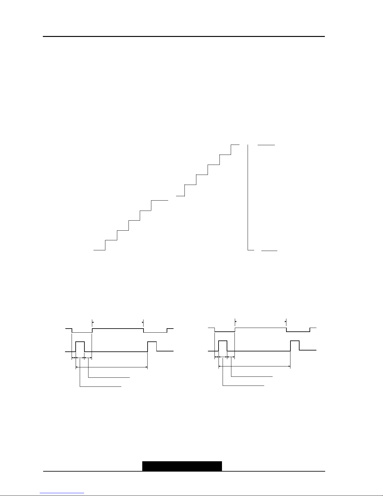
•Waveform
Video input(R.G.B)
--3--
L70S Technical Service Manual
ACTIVE (T4)
Front Porch
(T5) Period (T1)
Sync Width (T2)
Back Porch (T3)
ACTIVE (T4)
Front Porch
(T5) Period (T1)
Sync Width (T2)
Back Porch (T3)
• H-S nc • V-S nc
0
1
3
4
51
5
53
54
55 700mV
0mV
• Signal: 56 level gray
scale
• Linear stepping:
( .73mV ~ 56 Steps)
--4--
Video Input Terminal
A 15 Pin D-sub connector is used as the input signal connector
Pin and input signals are shown in the table below.
Pin Description
D-Sub miniature connector
SIGNAL
PIN NO.
3
1
5
4
6
7
8
9
10
11
1
13
14
SEPARATE SYNC/
DDC 1/ B
RED
GREEN
BLUE
GND
RETURN
RED GROUND
GREEN GROUND
BLUE GROUND
N.C
LOGIC GROUND
GROUND
SDA
H-SYNC(TTL)
V-SYNC(VCLK)
15 SCL

Connecting with External Equipment
Cautions
Be sure to turn off the power of your computer before connecting the monitor.
--5--
L70S Technical Service Manual
LINE OUT

--6--
Theor of Operation
1. AC/DC INVERTER
Input voltage : DC 1 V
Input current : .0A(Max)
Output current : 6.5mArms(TYP)
Frequency(switching) : 47KHz(Max)
Output power : 18W(TYP)
On/off control voltage : 5.0V
2. AC/DC ADATOR
This display device shall maintain the specified per formances in the range de scribed
below
Frequency : 50/60Hz
Voltage : 90 - 64Vac RMS
The following consumption requirments shall be met:
Power Consumption : 35W(typ)
Current consumption : < 1.0 Aac RMS
Output Specification:
output1 : 1 V/ A
output : 5V/1.5A
3. Audio S stem
This monitor has a audio system including two micro loudspeakers.
Each of two micro loudspeakers has a W(Max) output power.
This system also supports a headphone(earphone) output.
- Auto Signal Input : < 600mVp-p(Max.)
- Auto Amplifiers
W+ W Amplifier with DC Volume Control (for two micro loudspeakers)
RL=8 @THD=10% Vcc=14V (min. 10V, max. 18V)
Dual-Audio Power Amplifier (for a headphone output)
RL=3 @THD=10% Vcc=4.5V (min. 1.8V, max. 15V)
- Speaker
Micro Loudspeaker Spec.
Normal impedance 8 15% at 1.0V 1.5KHz
Resonance Freq. 550Hz +/- 110Hz at 1.0V
Freq. Range fo ~ 0KHz
Power Rating Normal 1.0W/Peak .0W
4. DPMS MODE
Status
on Pulse Pulse Active
Blank
No
Pulse
No
Pulse
off
Signal Power
Consumption
-
Within 3
Sec
Recovery
Time
Orange
LED
Indicator
Green
35W(typ)
1W (TYP) 30V AC
H-Sync V-Sync Video
--7--
L70S Technical Service Manual
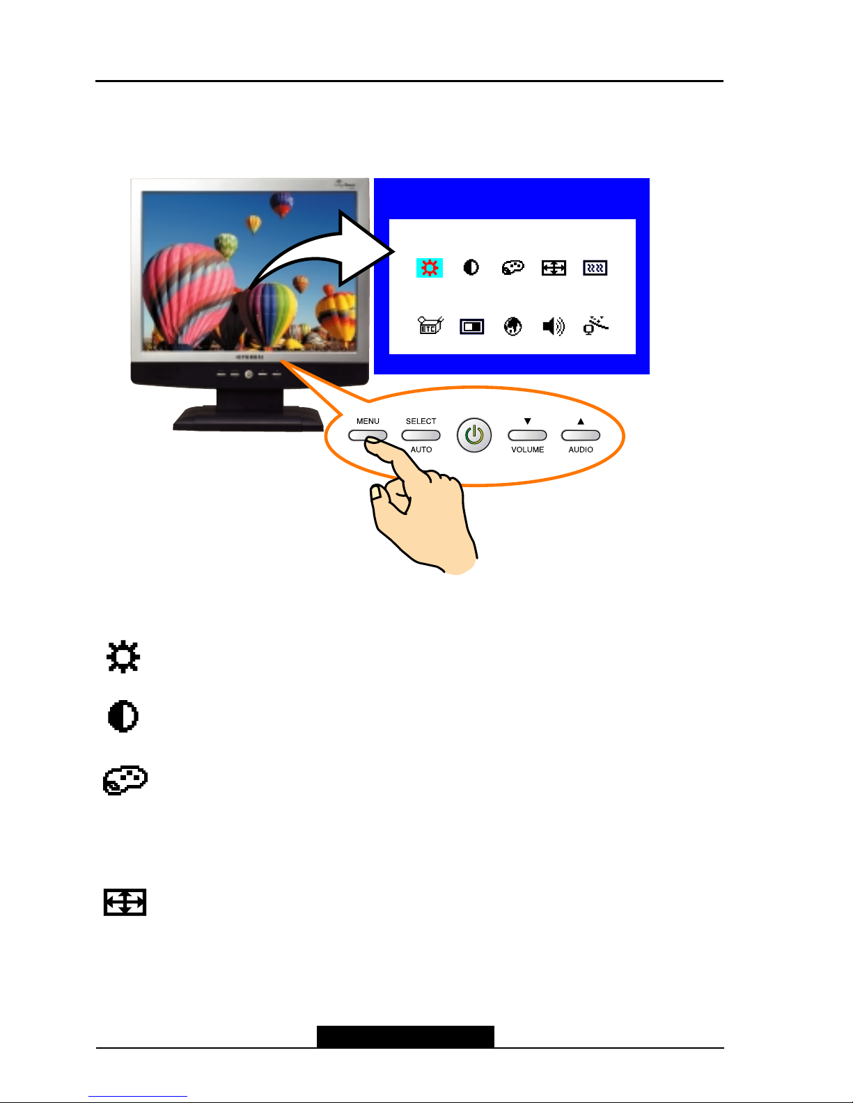
On Screen Controls & LED Indicator
The menu for screen setting adjustment is located in the OSD and can be viewed in one of
five languages OSD feature andmain funcrions are as follows:
he OSD adjustments available to you are listed below.
BRIGHTNESS
Adjust the brightness of the screen.
CONTRAST
Adjust the contrast of the screen.
COLOR CONTROL
Color temperature affects the tint of the image. With lower color
temperatures the image turns reddish and with higher temperatures
bluish.
There are three color settings available: Mode 1(9300K), Mode 2(6500K) or USER. With
the USER setting you can set individual values for red, green and blue.
POSITION
H POSITION
Adjusts the horizontal position of the entire screen image.
V POSITION
Adjusts the vertical position of the entire screen image.
1280x1024
H:63.9 V:60.0
BRIGHTNESSBRIGHTNESS

--8--
CLOCK PHASE
PHASE
Adjust the noise of the screen image.
CLOCK
Adjust the horizontal size of the entire screen image.
MISCELLANEOUS
RECALL
Recall the saved color data.
OSD TIMER
You can set the displayed time of OSD Menu window on the screen by using this
adjustment.
OSD POSITION
Adjust the OSD menu's horizontal or vertical position on the screen.
AUTO COLOR
Optimum color setting is auto programmed for user’s convenience.
LANGUAGE
You can select the language in which adjustment menus are displayed.
The following languages are available : English, French, German, Italian,
Spanish, Swedish, Finnish, Danish, Portuguese, Dutch and Japanese or chinese.
AUDIO
VOLUME
Adjust the audio volume level.
AUDIO
This menu is used to choose audio on or off.
AUTO ADJUST
You can adjust the shape of screen automatically at the full screen pattern.
--9--
L70S Technical Service Manual
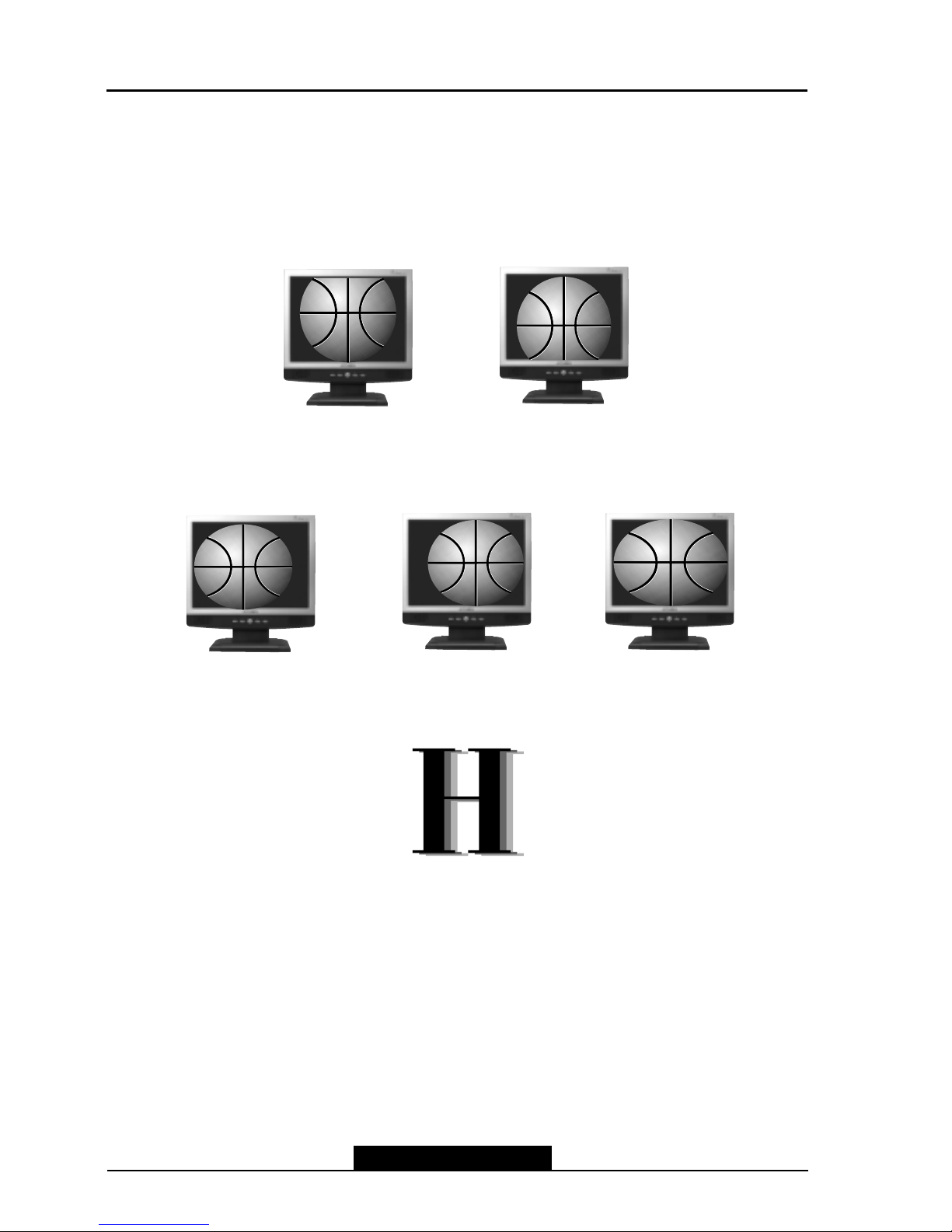
Getting Fine Picture
Step 1. At first Display, a full screen, such as, Window's background or "H" character should
be achieved by using Editor (ex: Notepad. exe)
Step 2. Adjust the screen to the center of the Display(LCD), by using the top and bottom
display controls. (i.e.Using V-Position Adjust menu)
Step 3. Adjust the screen to the center of the Display(LCD), by using the right and left
display controls. (i.e.Using Clock and H-Position adjust menu)
Step 4. Adjust the Clock-phase until the "H" Character displays clear.
Step 5. Using the Contrast. Brightness, and Color Control menu, set the color to your
preference.
Step 6. When you finish the adjustment, you can save your settings by pressing on the menu
until the OSD screen has disappeared.
Factor Setting & EEPROM Initialization Method
Factor Setting Method
- Connect the signal cable and power cable to the LCD monitor.
- Press Power switch with pressed MENU key.(Menu key + Power key).
- Then, a User can change the factory setting value in OSD menu.
- Save changed value and Turn off the power s/w.
- Turn on the power, adjust the screen.
Table of contents
Other ImageQuest Monitor manuals


