Infineon Technologies TLE5012B User manual

Sense & Control
User’s Manual
Rev. 1.2, 2018-02
User’s Manual
TLE5012B
Angle Sensor
GMR-Based Angle Sensor

Edition 2018-02
Published by
Infineon Technologies AG
81726 Munich, Germany
© 2018 Infineon Technologies AG
All Rights Reserved.
Legal Disclaimer
The information given in this document shall in no event be regarded as a guarantee of conditions or
characteristics. With respect to any examples or hints given herein, any typical values stated herein and/or any
information regarding the application of the device, Infineon Technologies hereby disclaims any and all warranties
and liabilities of any kind, including without limitation, warranties of non-infringement of intellectual property rights
of any third party.
Information
For further information on technology, delivery terms and conditions and prices, please contact the nearest
Infineon Technologies Office (www.infineon.com).
Warnings
Due to technical requirements, components may contain dangerous substances. For information on the types in
question, please contact the nearest Infineon Technologies Office.
Infineon Technologies components may be used in life-support devices or systems only with the express written
approval of Infineon Technologies, if a failure of such components can reasonably be expected to cause the failure
of that life-support device or system or to affect the safety or effectiveness of that device or system. Life support
devices or systems are intended to be implanted in the human body or to support and/or maintain and sustain
and/or protect human life. If they fail, it is reasonable to assume that the health of the user or other persons may
be endangered.

TLE5012B
User’s Manual 3 Rev. 1.2, 2018-02
Trademarks of Infineon Technologies AG
AURIX™, C166™, CanPAK™, CIPOS™, CIPURSE™, EconoPACK™, CoolMOS™, CoolSET™,
CORECONTROL™, CROSSAVE™, DAVE™, DI-POL™, EasyPIM™, EconoBRIDGE™, EconoDUAL™,
EconoPIM™, EconoPACK™, EiceDRIVER™, eupec™, FCOS™, HITFET™, HybridPACK™, I²RF™,
ISOFACE™, IsoPACK™, MIPAQ™, ModSTACK™, my-d™, NovalithIC™, OptiMOS™, ORIGA™,
POWERCODE™; PRIMARION™, PrimePACK™, PrimeSTACK™, PRO-SIL™, PROFET™, RASIC™,
ReverSave™, SatRIC™, SIEGET™, SINDRION™, SIPMOS™, SmartLEWIS™, SOLID FLASH™, TEMPFET™,
thinQ!™, TRENCHSTOP™, TriCore™.
Other Trademarks
Advance Design System™ (ADS) of Agilent Technologies, AMBA™, ARM™, MULTI-ICE™, KEIL™,
PRIMECELL™, REALVIEW™, THUMB™, µVision™ of ARM Limited, UK. AUTOSAR™ is licensed by AUTOSAR
development partnership. Bluetooth™ of Bluetooth SIG Inc. CAT-iq™ of DECT Forum. COLOSSUS™,
FirstGPS™ of Trimble Navigation Ltd. EMV™ of EMVCo, LLC (Visa Holdings Inc.). EPCOS™ of Epcos AG.
FLEXGO™ of Microsoft Corporation. FlexRay™ is licensed by FlexRay Consortium. HYPERTERMINAL™ of
Hilgraeve Incorporated. IEC™ of Commission Electrotechnique Internationale. IrDA™ of Infrared Data
Association Corporation. ISO™ of INTERNATIONAL ORGANIZATION FOR STANDARDIZATION. MATLAB™ of
MathWorks, Inc. MAXIM™ of Maxim Integrated Products, Inc. MICROTEC™, NUCLEUS™ of Mentor Graphics
Corporation. MIPI™ of MIPI Alliance, Inc. MIPS™ of MIPS Technologies, Inc., USA. muRata™ of MURATA
MANUFACTURING CO., MICROWAVE OFFICE™ (MWO) of Applied Wave Research Inc., OmniVision™ of
OmniVision Technologies, Inc. Openwave™ Openwave Systems Inc. RED HAT™ Red Hat, Inc. RFMD™ RF
Micro Devices, Inc. SIRIUS™ of Sirius Satellite Radio Inc. SOLARIS™ of Sun Microsystems, Inc. SPANSION™
of Spansion LLC Ltd. Symbian™ of Symbian Software Limited. TAIYO YUDEN™ of Taiyo Yuden Co.
TEAKLITE™ of CEVA, Inc. TEKTRONIX™ of Tektronix Inc. TOKO™ of TOKO KABUSHIKI KAISHA TA. UNIX™
of X/Open Company Limited. VERILOG™, PALLADIUM™ of Cadence Design Systems, Inc. VLYNQ™ of Texas
Instruments Incorporated. VXWORKS™, WIND RIVER™ of WIND RIVER SYSTEMS, INC. ZETEX™ of Diodes
Zetex Limited.
Last Trademarks Update 2011-11-11
Revision History
Page or Item Subjects (major changes since previous revision)
Rev. 1.2, 2018-02
Chapter 5.2.4 Update STAT and RESP in CRC calculation
Chapter 6.1.4 Add explanation when ANG_DIR = 1
Figure 6-1 Update STAT register
Chapter 3 Uptade Chapter 3
Chapter 5.6 Add footnote regarding maximum rotation speed
Chapter 6.2.1 Update S_MAGOL definition

TLE5012B
Table of Contents
User’s Manual 4 Rev. 1.2, 2018-02
Table of Contents . . . . . . . . . . . . . . . . . . . . . . . . . . . . . . . . . . . . . . . . . . . . . . . . . . . . . . . . . . . . . . . . 4
List of Figures . . . . . . . . . . . . . . . . . . . . . . . . . . . . . . . . . . . . . . . . . . . . . . . . . . . . . . . . . . . . . . . . . . . 6
List of Tables . . . . . . . . . . . . . . . . . . . . . . . . . . . . . . . . . . . . . . . . . . . . . . . . . . . . . . . . . . . . . . . . . . . . 8
1 Product Description . . . . . . . . . . . . . . . . . . . . . . . . . . . . . . . . . . . . . . . . . . . . . . . . . . . . . . . . . . . . . . 9
1.1 Overview . . . . . . . . . . . . . . . . . . . . . . . . . . . . . . . . . . . . . . . . . . . . . . . . . . . . . . . . . . . . . . . . . . . . . . . . 9
1.2 Features . . . . . . . . . . . . . . . . . . . . . . . . . . . . . . . . . . . . . . . . . . . . . . . . . . . . . . . . . . . . . . . . . . . . . . . 10
1.3 Application Example . . . . . . . . . . . . . . . . . . . . . . . . . . . . . . . . . . . . . . . . . . . . . . . . . . . . . . . . . . . . . . 10
2 Functional Description . . . . . . . . . . . . . . . . . . . . . . . . . . . . . . . . . . . . . . . . . . . . . . . . . . . . . . . . . . . 11
2.1 Block Diagram . . . . . . . . . . . . . . . . . . . . . . . . . . . . . . . . . . . . . . . . . . . . . . . . . . . . . . . . . . . . . . . . . . 11
2.2 Functional Block Description . . . . . . . . . . . . . . . . . . . . . . . . . . . . . . . . . . . . . . . . . . . . . . . . . . . . . . . 11
2.2.1 Internal Power Supply . . . . . . . . . . . . . . . . . . . . . . . . . . . . . . . . . . . . . . . . . . . . . . . . . . . . . . . . . . . 11
2.2.2 Oscillator and PLL . . . . . . . . . . . . . . . . . . . . . . . . . . . . . . . . . . . . . . . . . . . . . . . . . . . . . . . . . . . . . . 11
2.2.3 SD-ADC . . . . . . . . . . . . . . . . . . . . . . . . . . . . . . . . . . . . . . . . . . . . . . . . . . . . . . . . . . . . . . . . . . . . . . 12
2.2.4 Digital Signal Processing Unit . . . . . . . . . . . . . . . . . . . . . . . . . . . . . . . . . . . . . . . . . . . . . . . . . . . . . 12
2.2.5 Interfaces . . . . . . . . . . . . . . . . . . . . . . . . . . . . . . . . . . . . . . . . . . . . . . . . . . . . . . . . . . . . . . . . . . . . . 13
2.2.6 Safety Features . . . . . . . . . . . . . . . . . . . . . . . . . . . . . . . . . . . . . . . . . . . . . . . . . . . . . . . . . . . . . . . . 13
2.3 Sensing Principle . . . . . . . . . . . . . . . . . . . . . . . . . . . . . . . . . . . . . . . . . . . . . . . . . . . . . . . . . . . . . . . . 14
2.4 Pin Configuration . . . . . . . . . . . . . . . . . . . . . . . . . . . . . . . . . . . . . . . . . . . . . . . . . . . . . . . . . . . . . . . . 16
2.5 Pin Description . . . . . . . . . . . . . . . . . . . . . . . . . . . . . . . . . . . . . . . . . . . . . . . . . . . . . . . . . . . . . . . . . . 16
3 Application Circuits . . . . . . . . . . . . . . . . . . . . . . . . . . . . . . . . . . . . . . . . . . . . . . . . . . . . . . . . . . . . . 17
3.1 IIF interface and SSC (IIF in push-pull configuration) . . . . . . . . . . . . . . . . . . . . . . . . . . . . . . . . . . . . . 17
3.2 HSM interface and SSC (HSM in push-pull configuration) . . . . . . . . . . . . . . . . . . . . . . . . . . . . . . . . . 17
3.3 HSM interface and SSC (HSM in open-drain configuration) . . . . . . . . . . . . . . . . . . . . . . . . . . . . . . . . 18
3.4 PWM interface (push-pull configuration) . . . . . . . . . . . . . . . . . . . . . . . . . . . . . . . . . . . . . . . . . . . . . . . 18
3.5 PWM interface (open-drain configuration) . . . . . . . . . . . . . . . . . . . . . . . . . . . . . . . . . . . . . . . . . . . . . 19
3.6 SPC interface . . . . . . . . . . . . . . . . . . . . . . . . . . . . . . . . . . . . . . . . . . . . . . . . . . . . . . . . . . . . . . . . . . . 19
3.7 SSC interface (push-pull configuration) . . . . . . . . . . . . . . . . . . . . . . . . . . . . . . . . . . . . . . . . . . . . . . . 20
3.8 SSC interface (open-drain configuration) . . . . . . . . . . . . . . . . . . . . . . . . . . . . . . . . . . . . . . . . . . . . . . 20
3.9 Sensor supply in bus mode . . . . . . . . . . . . . . . . . . . . . . . . . . . . . . . . . . . . . . . . . . . . . . . . . . . . . . . . 21
4 Specification . . . . . . . . . . . . . . . . . . . . . . . . . . . . . . . . . . . . . . . . . . . . . . . . . . . . . . . . . . . . . . . . . . . 22
4.1 Autocalibration . . . . . . . . . . . . . . . . . . . . . . . . . . . . . . . . . . . . . . . . . . . . . . . . . . . . . . . . . . . . . . . . . . 22
4.1.1 Angle Error adder with Autocalibration enabled . . . . . . . . . . . . . . . . . . . . . . . . . . . . . . . . . . . . . . . 25
4.2 Prediction mode . . . . . . . . . . . . . . . . . . . . . . . . . . . . . . . . . . . . . . . . . . . . . . . . . . . . . . . . . . . . . . . . . 26
4.3 Calculation of the Junction Temperature . . . . . . . . . . . . . . . . . . . . . . . . . . . . . . . . . . . . . . . . . . . . . . 27
4.4 Calculation of the Temperature . . . . . . . . . . . . . . . . . . . . . . . . . . . . . . . . . . . . . . . . . . . . . . . . . . . . . 27
4.5 Switching to external clock . . . . . . . . . . . . . . . . . . . . . . . . . . . . . . . . . . . . . . . . . . . . . . . . . . . . . . . . . 28
5 Interfaces . . . . . . . . . . . . . . . . . . . . . . . . . . . . . . . . . . . . . . . . . . . . . . . . . . . . . . . . . . . . . . . . . . . . . . 29
5.1 Interfaces overview . . . . . . . . . . . . . . . . . . . . . . . . . . . . . . . . . . . . . . . . . . . . . . . . . . . . . . . . . . . . . . . 29
5.2 Synchronous Serial Communication (SSC) Interface . . . . . . . . . . . . . . . . . . . . . . . . . . . . . . . . . . . . . 31
5.2.1 SSC Timing Definition . . . . . . . . . . . . . . . . . . . . . . . . . . . . . . . . . . . . . . . . . . . . . . . . . . . . . . . . . . . 31
5.2.2 SSC Data Transfer . . . . . . . . . . . . . . . . . . . . . . . . . . . . . . . . . . . . . . . . . . . . . . . . . . . . . . . . . . . . . 33
5.2.3 TLE5012B in bus mode . . . . . . . . . . . . . . . . . . . . . . . . . . . . . . . . . . . . . . . . . . . . . . . . . . . . . . . . . . 36
5.2.4 Cyclic Redundancy Check (CRC) . . . . . . . . . . . . . . . . . . . . . . . . . . . . . . . . . . . . . . . . . . . . . . . . . . 37
5.2.5 Angle Calculation with X-raw and Y-raw values . . . . . . . . . . . . . . . . . . . . . . . . . . . . . . . . . . . . . . . 43
5.2.5.1 Angle Calculation using pre-calibrated compensation values . . . . . . . . . . . . . . . . . . . . . . . . . . . 43
5.2.5.2 Angle Calculation with end-of-line calibration values . . . . . . . . . . . . . . . . . . . . . . . . . . . . . . . . . . 45
Table of Contents

TLE5012B
Table of Contents
User’s Manual 5 Rev. 1.2, 2018-02
5.3 Pulse Width Modulation Interface . . . . . . . . . . . . . . . . . . . . . . . . . . . . . . . . . . . . . . . . . . . . . . . . . . . . 46
5.4 Short PWM Code (SPC) . . . . . . . . . . . . . . . . . . . . . . . . . . . . . . . . . . . . . . . . . . . . . . . . . . . . . . . . . . . 48
5.4.1 Unit Time Setup . . . . . . . . . . . . . . . . . . . . . . . . . . . . . . . . . . . . . . . . . . . . . . . . . . . . . . . . . . . . . . . . 50
5.4.2 Master Trigger Pulse Requirements . . . . . . . . . . . . . . . . . . . . . . . . . . . . . . . . . . . . . . . . . . . . . . . . 51
5.4.3 Checksum Nibble Details . . . . . . . . . . . . . . . . . . . . . . . . . . . . . . . . . . . . . . . . . . . . . . . . . . . . . . . . . 52
5.5 Hall Switch Mode (HSM) . . . . . . . . . . . . . . . . . . . . . . . . . . . . . . . . . . . . . . . . . . . . . . . . . . . . . . . . . . . 55
5.6 Incremental Interface (IIF) . . . . . . . . . . . . . . . . . . . . . . . . . . . . . . . . . . . . . . . . . . . . . . . . . . . . . . . . . 59
6 SSC Registers . . . . . . . . . . . . . . . . . . . . . . . . . . . . . . . . . . . . . . . . . . . . . . . . . . . . . . . . . . . . . . . . . . 64
6.1 Registers Overview . . . . . . . . . . . . . . . . . . . . . . . . . . . . . . . . . . . . . . . . . . . . . . . . . . . . . . . . . . . . . . . 64
6.1.1 Bit Types . . . . . . . . . . . . . . . . . . . . . . . . . . . . . . . . . . . . . . . . . . . . . . . . . . . . . . . . . . . . . . . . . . . . . 67
6.1.2 Communication Examples . . . . . . . . . . . . . . . . . . . . . . . . . . . . . . . . . . . . . . . . . . . . . . . . . . . . . . . . 68
6.1.3 Signed registers and Two’s complement . . . . . . . . . . . . . . . . . . . . . . . . . . . . . . . . . . . . . . . . . . . . . 70
6.1.4 Zero position configuration . . . . . . . . . . . . . . . . . . . . . . . . . . . . . . . . . . . . . . . . . . . . . . . . . . . . . . . 71
6.2 Registers Descriptions . . . . . . . . . . . . . . . . . . . . . . . . . . . . . . . . . . . . . . . . . . . . . . . . . . . . . . . . . . . . 73
6.2.1 Register Descriptions . . . . . . . . . . . . . . . . . . . . . . . . . . . . . . . . . . . . . . . . . . . . . . . . . . . . . . . . . . . 75
7 Pre-Configured Derivates . . . . . . . . . . . . . . . . . . . . . . . . . . . . . . . . . . . . . . . . . . . . . . . . . . . . . . . 102
7.1 IIF-type: E1000 . . . . . . . . . . . . . . . . . . . . . . . . . . . . . . . . . . . . . . . . . . . . . . . . . . . . . . . . . . . . . . . . . 102
7.2 HSM-type: E3005 . . . . . . . . . . . . . . . . . . . . . . . . . . . . . . . . . . . . . . . . . . . . . . . . . . . . . . . . . . . . . . . 102
7.3 PWM-type: E5000 . . . . . . . . . . . . . . . . . . . . . . . . . . . . . . . . . . . . . . . . . . . . . . . . . . . . . . . . . . . . . . . 102
7.4 PWM-type: E5020 . . . . . . . . . . . . . . . . . . . . . . . . . . . . . . . . . . . . . . . . . . . . . . . . . . . . . . . . . . . . . . . 103
7.5 SPC-type: E9000 . . . . . . . . . . . . . . . . . . . . . . . . . . . . . . . . . . . . . . . . . . . . . . . . . . . . . . . . . . . . . . . 103
7.6 Fuse Values . . . . . . . . . . . . . . . . . . . . . . . . . . . . . . . . . . . . . . . . . . . . . . . . . . . . . . . . . . . . . . . . . . . 104

TLE5012B
List of Figures
User’s Manual 6 Rev. 1.2, 2018-02
Figure 1-1 PG-DSO-8 package . . . . . . . . . . . . . . . . . . . . . . . . . . . . . . . . . . . . . . . . . . . . . . . . . . . . . . . . . . . . . 9
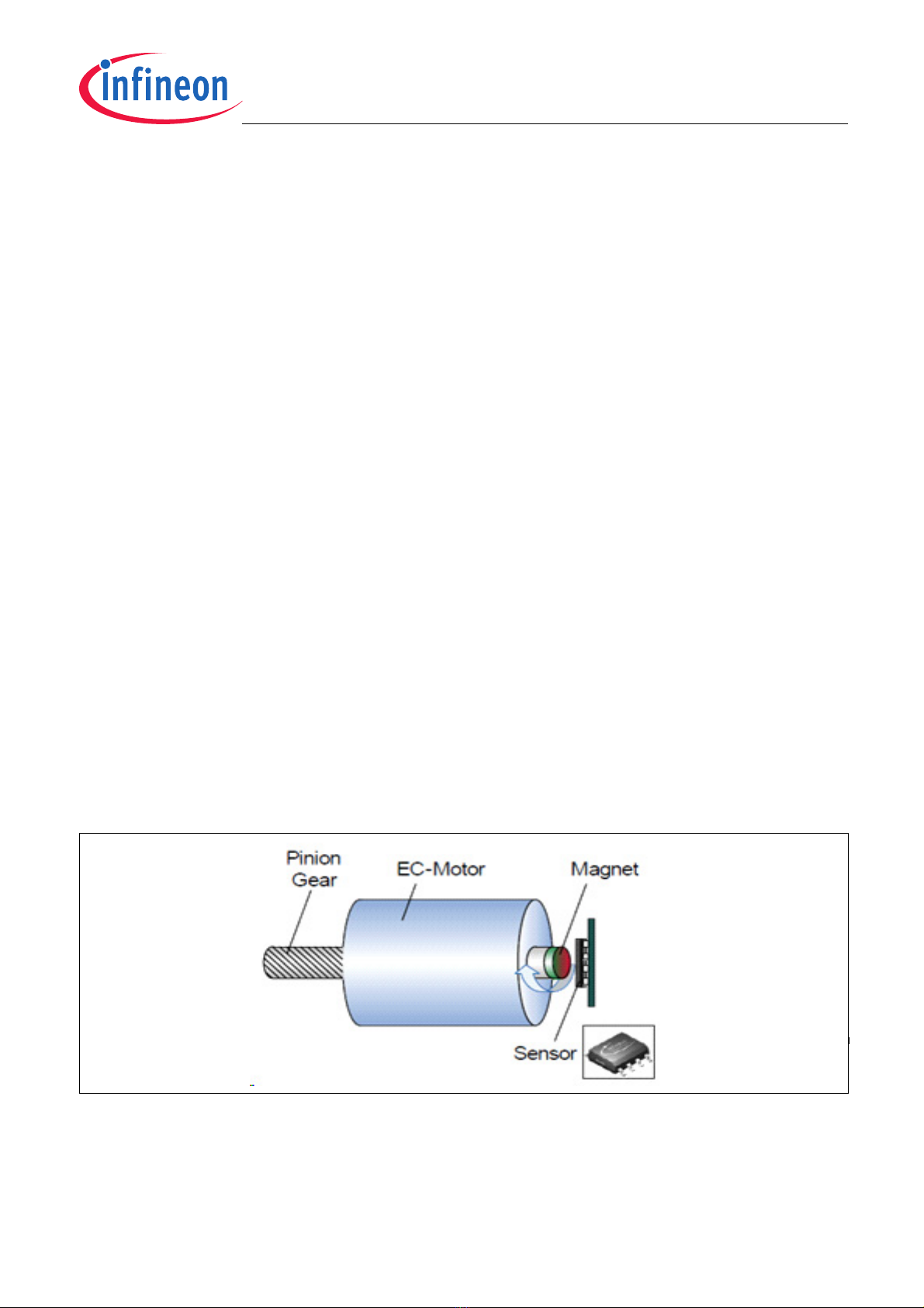
Figure 1-2 A usual application for TLE5012B is the electrically commutated motor . . . . . . . . . . . . . . . . . . . . 10
Figure 2-1 TLE5012B block diagram . . . . . . . . . . . . . . . . . . . . . . . . . . . . . . . . . . . . . . . . . . . . . . . . . . . . . . . . 11
Figure 2-2 Laser Fuses burning process . . . . . . . . . . . . . . . . . . . . . . . . . . . . . . . . . . . . . . . . . . . . . . . . . . . . . 12
Figure 2-3 PRO-SILTM Logo. . . . . . . . . . . . . . . . . . . . . . . . . . . . . . . . . . . . . . . . . . . . . . . . . . . . . . . . . . . . . . . 13
Figure 2-4 Sensitive bridges of the GMR sensor (not to scale) . . . . . . . . . . . . . . . . . . . . . . . . . . . . . . . . . . . . 14
Figure 2-5 Ideal output of the GMR sensor bridges . . . . . . . . . . . . . . . . . . . . . . . . . . . . . . . . . . . . . . . . . . . . . 15
Figure 2-6 Pin configuration (top view) . . . . . . . . . . . . . . . . . . . . . . . . . . . . . . . . . . . . . . . . . . . . . . . . . . . . . . 16
Figure 3-1 Application circuit for TLE5012B with IIF interface and SSC . . . . . . . . . . . . . . . . . . . . . . . . . . . . . 17
Figure 3-2 Application circuit for TLE5012B with HSM interface (push-pull configuration) and SSC . . . . . . . 17
Figure 3-3 Application circuit for TLE5012B with HSM interface (open-drain configuration) and SSC . . . . . . 18
Figure 3-4 Application circuit for TLE5012B with PWM (push-pull configuration) interface. . . . . . . . . . . . . . . 18
Figure 3-5 Application circuit for TLE5012B with PWM (open-drain configuration) interface . . . . . . . . . . . . . 19
Figure 3-6 Application circuit for TLE5012B with SPC interface . . . . . . . . . . . . . . . . . . . . . . . . . . . . . . . . . . . 19
Figure 3-7 SSC interface with push-pull configuration (high-speed application) . . . . . . . . . . . . . . . . . . . . . . . 20
Figure 3-8 SSC interface with open-drain configuration (bus systems) . . . . . . . . . . . . . . . . . . . . . . . . . . . . . . 20
Figure 3-9 Sensors’ supply in bus mode . . . . . . . . . . . . . . . . . . . . . . . . . . . . . . . . . . . . . . . . . . . . . . . . . . . . . 21
Figure 4-1 Parameter correction with autocalibration mode 1 . . . . . . . . . . . . . . . . . . . . . . . . . . . . . . . . . . . . . 22
Figure 4-2 Parameter correction with autocalibration mode 2 . . . . . . . . . . . . . . . . . . . . . . . . . . . . . . . . . . . . . 22
Figure 4-3 Parameter correction with autocalibration mode 3 . . . . . . . . . . . . . . . . . . . . . . . . . . . . . . . . . . . . . 23
Figure 4-4 Cases where an angle error adder has to be included if autocalibration is enabled . . . . . . . . . . . 25
Figure 4-5 Delay of sensor output . . . . . . . . . . . . . . . . . . . . . . . . . . . . . . . . . . . . . . . . . . . . . . . . . . . . . . . . . . 26
Figure 4-6 Revolution counter with prediction mode disabled/enabled . . . . . . . . . . . . . . . . . . . . . . . . . . . . . . 26
Figure 5-1 SSC timing . . . . . . . . . . . . . . . . . . . . . . . . . . . . . . . . . . . . . . . . . . . . . . . . . . . . . . . . . . . . . . . . . . . 31
Figure 5-2 SSC data transfer (data-read example) . . . . . . . . . . . . . . . . . . . . . . . . . . . . . . . . . . . . . . . . . . . . . 33
Figure 5-3 SSC data transfer (data-write example) . . . . . . . . . . . . . . . . . . . . . . . . . . . . . . . . . . . . . . . . . . . . . 33
Figure 5-4 SSC bit ordering (read example) . . . . . . . . . . . . . . . . . . . . . . . . . . . . . . . . . . . . . . . . . . . . . . . . . . 35
Figure 5-5 Update of update registers . . . . . . . . . . . . . . . . . . . . . . . . . . . . . . . . . . . . . . . . . . . . . . . . . . . . . . . 35
Figure 5-6 Example of four slaves connected to a bus with one master with SSC interface . . . . . . . . . . . . . . 36
Figure 5-7 Fast CRC polynomial division circuit . . . . . . . . . . . . . . . . . . . . . . . . . . . . . . . . . . . . . . . . . . . . . . . 37
Figure 5-8 TLE5012B’s CRC generator polynomial for the SSC interface . . . . . . . . . . . . . . . . . . . . . . . . . . . 37
Figure 5-9 CRC generation example with SSC interface. . . . . . . . . . . . . . . . . . . . . . . . . . . . . . . . . . . . . . . . . 38
Figure 5-10 Flow-Chart of Angle Calculation from the X-raw and Y-raw values . . . . . . . . . . . . . . . . . . . . . . . . 45
Figure 5-11 Typical example of a PWM signal. . . . . . . . . . . . . . . . . . . . . . . . . . . . . . . . . . . . . . . . . . . . . . . . . . 46
Figure 5-12 Example of four slaves connected to a bus with one master with SPC interface . . . . . . . . . . . . . . 48
Figure 5-13 SPC frame example . . . . . . . . . . . . . . . . . . . . . . . . . . . . . . . . . . . . . . . . . . . . . . . . . . . . . . . . . . . . 49
Figure 5-14 SPC pause timing diagram . . . . . . . . . . . . . . . . . . . . . . . . . . . . . . . . . . . . . . . . . . . . . . . . . . . . . . . 49
Figure 5-15 SPC configuration in open drain mode . . . . . . . . . . . . . . . . . . . . . . . . . . . . . . . . . . . . . . . . . . . . . . 49
Figure 5-16 SPC Master pulse timing . . . . . . . . . . . . . . . . . . . . . . . . . . . . . . . . . . . . . . . . . . . . . . . . . . . . . . . . 51
Figure 5-17 TLE5012B’s CRC generator polynomial for the SPC interface . . . . . . . . . . . . . . . . . . . . . . . . . . . 52
Figure 5-18 CRC generation example with SPC interface. . . . . . . . . . . . . . . . . . . . . . . . . . . . . . . . . . . . . . . . . 52
Figure 5-19 Hall Switch Mode . . . . . . . . . . . . . . . . . . . . . . . . . . . . . . . . . . . . . . . . . . . . . . . . . . . . . . . . . . . . . . 55
Figure 5-20 HS hysteresis . . . . . . . . . . . . . . . . . . . . . . . . . . . . . . . . . . . . . . . . . . . . . . . . . . . . . . . . . . . . . . . . . 58
Figure 5-21 Incremental interface with A/B mode . . . . . . . . . . . . . . . . . . . . . . . . . . . . . . . . . . . . . . . . . . . . . . . 59
Figure 5-22 Incremental interface with Step/Direction mode . . . . . . . . . . . . . . . . . . . . . . . . . . . . . . . . . . . . . . . 59
Figure 5-23 Increcremental Interface startup pulses and first step movements at different speeds . . . . . . . . . 60
Figure 5-24 Increcremental Interface startup pulses frequency. . . . . . . . . . . . . . . . . . . . . . . . . . . . . . . . . . . . . 61
Figure 5-25 IIF Index pulse in A/B Mode . . . . . . . . . . . . . . . . . . . . . . . . . . . . . . . . . . . . . . . . . . . . . . . . . . . . . . 61
Figure 5-26 IIF Index pulse in Step/Direction Mode. . . . . . . . . . . . . . . . . . . . . . . . . . . . . . . . . . . . . . . . . . . . . . 62
List of Figures

TLE5012B
List of Figures
User’s Manual 7 Rev. 1.2, 2018-02
Figure 5-27 Phase A/B output during a rotation direction change due to the hysteresis threshold . . . . . . . . . . 62
Figure 6-1 Bitmap Part 1 . . . . . . . . . . . . . . . . . . . . . . . . . . . . . . . . . . . . . . . . . . . . . . . . . . . . . . . . . . . . . . . . . 64
Figure 6-2 Bitmap Part 2 . . . . . . . . . . . . . . . . . . . . . . . . . . . . . . . . . . . . . . . . . . . . . . . . . . . . . . . . . . . . . . . . . 65
Figure 6-3 Colour legend for the Bitmap . . . . . . . . . . . . . . . . . . . . . . . . . . . . . . . . . . . . . . . . . . . . . . . . . . . . . 65
Figure 6-4 SSC command to read angle value . . . . . . . . . . . . . . . . . . . . . . . . . . . . . . . . . . . . . . . . . . . . . . . . 68
Figure 6-5 SSC command to read angle speed and angle revolution . . . . . . . . . . . . . . . . . . . . . . . . . . . . . . . 68
Figure 6-6 SSC command to change Interface Mode2 register. . . . . . . . . . . . . . . . . . . . . . . . . . . . . . . . . . . . 68
Figure 6-7 SSC data transfer sequence to change a configuration parameter . . . . . . . . . . . . . . . . . . . . . . . . 69
Figure 6-8 Example of a SSC data transfer sequence to change a configuration parameter . . . . . . . . . . . . . 69
Figure 6-9 Flow-Chart of ANG_BASE calibration procedure . . . . . . . . . . . . . . . . . . . . . . . . . . . . . . . . . . . . . . 71
Figure 6-10 SSC data transfer to configure the zero position . . . . . . . . . . . . . . . . . . . . . . . . . . . . . . . . . . . . . . 72
Figure 6-11 Zero position configuration in different domains. . . . . . . . . . . . . . . . . . . . . . . . . . . . . . . . . . . . . . . 72
Figure 6-12 Timing of angle calculation in SPC. Trigger Nibble low time corresponds to slave number. . . . . . 96
Figure 7-1 Derivate-specific fuse settings . . . . . . . . . . . . . . . . . . . . . . . . . . . . . . . . . . . . . . . . . . . . . . . . . . . 104

TLE5012B
List of Tables
User’s Manual 8 Rev. 1.2, 2018-02
Table 2-1 Pin Description . . . . . . . . . . . . . . . . . . . . . . . . . . . . . . . . . . . . . . . . . . . . . . . . . . . . . . . . . . . . . . . . 16
Table 4-1 Initialization via SSC / SPI to change ANG_DIR . . . . . . . . . . . . . . . . . . . . . . . . . . . . . . . . . . . . . . 24
Table 4-2 Additional angle error examples . . . . . . . . . . . . . . . . . . . . . . . . . . . . . . . . . . . . . . . . . . . . . . . . . . 25
Table 5-1 Main interface characteristics . . . . . . . . . . . . . . . . . . . . . . . . . . . . . . . . . . . . . . . . . . . . . . . . . . . . . 30
Table 5-2 SSC push-pull timing specification . . . . . . . . . . . . . . . . . . . . . . . . . . . . . . . . . . . . . . . . . . . . . . . . 31
Table 5-3 SSC open-drain timing specification . . . . . . . . . . . . . . . . . . . . . . . . . . . . . . . . . . . . . . . . . . . . . . . 32
Table 5-4 Structure of the Command Word . . . . . . . . . . . . . . . . . . . . . . . . . . . . . . . . . . . . . . . . . . . . . . . . . . 33
Table 5-5 Structure of the Safety Word . . . . . . . . . . . . . . . . . . . . . . . . . . . . . . . . . . . . . . . . . . . . . . . . . . . . . 34
Table 5-6 Bit Types . . . . . . . . . . . . . . . . . . . . . . . . . . . . . . . . . . . . . . . . . . . . . . . . . . . . . . . . . . . . . . . . . . . . 34
Table 5-7 PWM interface . . . . . . . . . . . . . . . . . . . . . . . . . . . . . . . . . . . . . . . . . . . . . . . . . . . . . . . . . . . . . . . . 47
Table 5-8 Frame configuration . . . . . . . . . . . . . . . . . . . . . . . . . . . . . . . . . . . . . . . . . . . . . . . . . . . . . . . . . . . . 50
Table 5-9 Structure of status nibble . . . . . . . . . . . . . . . . . . . . . . . . . . . . . . . . . . . . . . . . . . . . . . . . . . . . . . . . 50
Table 5-10 Predivider setting . . . . . . . . . . . . . . . . . . . . . . . . . . . . . . . . . . . . . . . . . . . . . . . . . . . . . . . . . . . . . . 50
Table 5-11 Master pulse parameters . . . . . . . . . . . . . . . . . . . . . . . . . . . . . . . . . . . . . . . . . . . . . . . . . . . . . . . . 51
Table 5-12 Hall Switch Mode . . . . . . . . . . . . . . . . . . . . . . . . . . . . . . . . . . . . . . . . . . . . . . . . . . . . . . . . . . . . . . 55
Table 5-13 Incremental Interface . . . . . . . . . . . . . . . . . . . . . . . . . . . . . . . . . . . . . . . . . . . . . . . . . . . . . . . . . . . 63
Table 6-1 Bit Types . . . . . . . . . . . . . . . . . . . . . . . . . . . . . . . . . . . . . . . . . . . . . . . . . . . . . . . . . . . . . . . . . . . . 67
Table 6-2 Register Overview . . . . . . . . . . . . . . . . . . . . . . . . . . . . . . . . . . . . . . . . . . . . . . . . . . . . . . . . . . . . . 73
List of Tables

TLE5012B
Product Description
User’s Manual 9 Rev. 1.2, 2018-02
1 Product Description
Figure 1-1 PG-DSO-8 package
1.1 Overview
The TLE5012B is a 360° angle sensor that detects the orientation of a magnetic field. This is achieved by
measuring sine and cosine angle components with monolithically integrated Giant Magneto Resistance (iGMR)
elements. These raw signals (sine and cosine) are digitally processed internally to calculate the angle orientation
of the magnetic field (magnet).
The TLE5012B is a pre-calibrated sensor. The calibration parameters are stored in laser fuses. At start-up the
values of the fuses are written into flip-flops, where these values can be changed to application-specific
parameters. The precision of the angle measurement, over a wide temperature range and a long lifetime, can be
improved by enabling an optional internal autocalibration algorithm.
Data communications are accomplished with a bi-directional Synchronous Serial Communication (SSC) that is
SPI-compatible. The sensor configuration is stored in registers, which are accessible by the SSC interface.
Additionally four other interfaces are available with the TLE5012B: Pulse-Width-Modulation (PWM) Protocol,
Short-PWM-Code (SPC) Protocol, Hall Switch Mode (HSM) and Incremental Interface (IIF). These interfaces can
be used in parallel with SSC or alone. Pre-configured sensor derivates with different interface settings are also
available. See the derivate ordering codes in the TLE5012B Data Sheet. A description of the derivates can also
be seen in Chapter 7.
Online diagnostic functions are provided to ensure reliable operation.
TLE5012B
Product Description
User’s Manual 10 Rev. 1.2, 2018-02
1.2 Features
•Giant Magneto Resistance (GMR)-based principle
• Integrated magnetic field sensing for angle measurement
• 360° angle measurement with revolution counter and angle speed measurement
• Two separate highly accurate single bit SD-ADC
• 15 bit representation of absolute angle value on the output (resolution of 0.01°)
• 16 bit representation of sine / cosine values on the interface
• Max. 1.0° angle error over lifetime and temperature-range with activated auto-calibration
• Bi-directional SSC Interface typ. 8Mbit/s
• Supports Safety Integrity Level (SIL) with diagnostic functions and status information
• Interfaces: SSC, PWM, Incremental Interface (IIF), Hall Switch Mode (HSM), Short PWM Code (SPC, based
on SENT protocol defined in SAE J2716)
• Output pins can be configured (programmed or pre-configured) as push-pull or open-drain
• Bus mode operation of multiple sensors on one line is possible with SSC or SPC interface in open-drain
configuration
•0.25μm CMOS technology
• Automotive qualified: -40°C to 150°C (junction temperature)
• ESD > 4kV (HBM)
• RoHS compliant (Pb-free package)
• Halogen-free
1.3 Application Example
The TLE5012B GMR-based angle sensor is designed for angular position sensing in automotive applications such
as:
• Electrically commutated motor (e.g. Electric Power Steering (EPS), Brushless DC electric motors (BLDC))
• Rotary switches
• Steering angle measurements
• General angular sensing
The TLE5012B is also used in various non-automotive applications.
Figure 1-2 A usual application for TLE5012B is the electrically commutated motor
M
TLE5012B
Functional Description
User’s Manual 11 Rev. 1.2, 2018-02
2 Functional Description
2.1 Block Diagram
Figure 2-1 TLE5012B block diagram
2.2 Functional Block Description
2.2.1 Internal Power Supply
The internal stages of the TLE5012B are supplied with several voltage regulators:
• GMR Voltage Regulator, VRG
• Analog Voltage Regulator, VRA
• Digital Voltage Regulator, VRD (derived from VRA)
These regulators are directly connected to the supply voltage VDD.
2.2.2 Oscillator and PLL
The digital clock of the TLE5012B is provided by the Phase-Locked Loop (PLL), which is by default fed by an
internal oscillator. In order to synchronize the TLE5012B with other ICs in a system, the TLE5012B can be
VRG VRA VRD
TLE5012B
V
DD
X
GMR
Y
GMR
Temp
SD-
ADC
SD-
ADC
SD-
ADC
Digital
Signal
Processing
Unit
CORDIC
CCU
RAM
SSC Interface
Incremental IF
PWM
HSM
SPC
CSQ
SCK
DATA
IFA
IFB
GND
IFC
Osc PLL
ISM
Fuses
TLE5012B
Functional Description
User’s Manual 12 Rev. 1.2, 2018-02
configured via SSC interface to use an external clock signal supplied on the IFC pin as the PLL source, instead of
the internal clock. External clock mode is only available in the PWM or SPC interface configurations.
2.2.3 SD-ADC
The Sigma-Delta Analog-Digital-Converters (SD-ADC) transform the analog GMR voltages and temperature
voltage into the digital domain.
2.2.4 Digital Signal Processing Unit
The Digital Signal Processing Unit (DSPU) contains the:
•Intelligent State Machine (ISM), which does error compensation of offset, offset temperature drift, amplitude
synchronicity and orthogonality of the raw signals from the GMR bridges, and performs additional features
such as auto-calibration, prediction and angle speed calculation
•COordinate Rotation DIgital Computer (CORDIC), which contains the trigonometric function for angle
calculation
•Capture Compare Unit (CCU), which is used to generate the PWM and SPC signals
•Random Access Memory (RAM), which contains the configuration registers
• Laser Fuses, which contain the calibration parameters for the error-compensation and the IC default
configuration, which is loaded into the RAM at startup
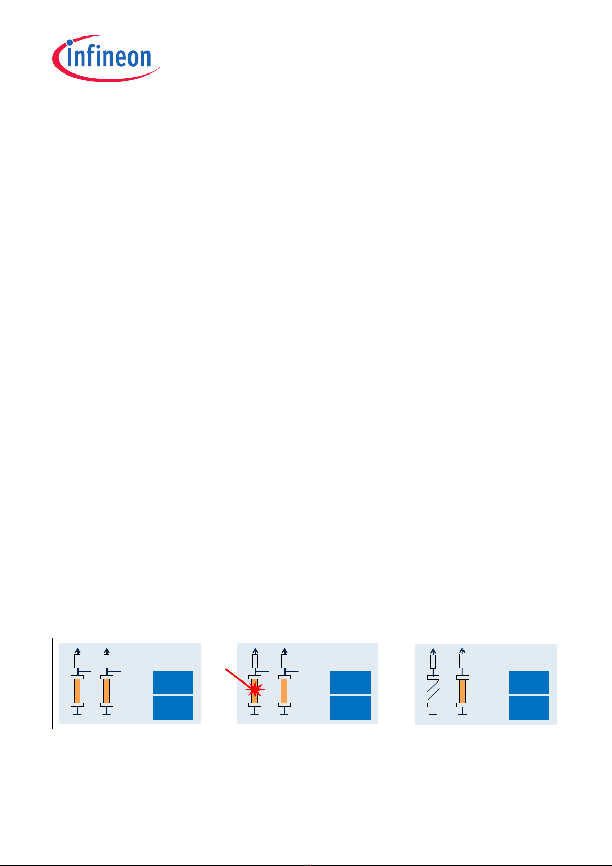
Laser fuses configuration
The laser fuse settings are derivate specific. During production, each and every TLE5012B chip is specifically
configured according to a derivate interface (PWM, SPC, HSM or IIF) and to its specific calibration values (e.g.
offset, amplitude synchronicity, orthogonality). These default values are set by laser fuses, where they remain
stored permanently. At power-on the values stored in the fuses are loaded into flip-flops (placed in the RAM).
Via the SSC interface, these derivate specific configuration values can be overwritten in the RAM. This allows
some programmability such as change of interface (using a IIF derivate as a PWM derivate for example) or to
correct the calibration values (if running the autocalibration mode for example). It is highly recommended to
configure the sensor with customized settings right after a Hardware reset (within the first 120µs, prior to start of
the Built-In Self-Test). If this interval is not sufficient, it is also possible to configure the sensor after the power-on
time. To ensure a correct configuration after power-on time, see recommendations on Chapter 6. When powered
off or reset, the overwritten values will be lost and the default values stored in the fuses will be reloaded into the
RAM at the next power up.
The Figure 2-2 shows how the fuse burning process works. In the original state all fuses are connected to ground
(GND). Once the calibration and derivate specific values are calculated, the information is burned into the fuses,
so that some remain connected to GND (“low” or logical “0”) and some are now pulled up by a resistor (“high” or
logical “1”). When powering the sensor, the RAM is initialized with the values from the fuses.
Figure 2-2 Laser Fuses burning process
DSPU
RAM
F
U
S
E
GND
0
F
U
S
E
GND
…
V
DD
0
V
DD
DSPU
RAM
F
U
S
E
GND
F
U
S
E
GND
…
0
V
DD
0
V
DD
DSPU
RAM
GND
F
U
S
E
GND
…
10
0
V
DD
1
V
DD

TLE5012B
Functional Description
User’s Manual 13 Rev. 1.2, 2018-02
2.2.5 Interfaces
Bi-directional communication with the TLE5012B is enabled by a three-wire SSC interface. In parallel to the SSC
interface, one secondary interface can be selected, which is available on the IFA, IFB, IFC pins:
•PWM
• Incremental Interface
• Hall Switch Mode
• Short PWM Code
By using pre-configured derivates (see Chapter 7), the TLE5012B can also be operated with the secondary
interface only, without SSC communication.
2.2.6 Safety Features
The TLE5012B offers a multiplicity of safety features to support the Safety Integrity Level (SIL). Infineon’s sensors
that are intended for this purpose are identified by the following logo:
Figure 2-3 PRO-SILTM Logo
Disclaimer
PRO-SIL™ is a Registered Trademark of Infineon Technologies AG.
The PRO-SIL™ Trademark designates Infineon products which contain SIL Supporting Features.
SIL Supporting Features are intended to support the overall System Design to reach the desired SIL (according
to IEC61508) or A-SIL (according to ISO26262) level for the Safety System with high efficiency.
SIL respectively A-SIL certification for such a System has to be reached on system level by the System
Responsible at an accredited Certification Authority.
SIL stands for Safety Integrity Level (according to IEC 61508)
A-SIL stands for Automotive-Safety Integrity Level (according to ISO 26262)
Safety features are:
• Test vectors switchable to ADC input (activated via SSC interface)
• Inversion or combination of filter input streams (activated via SSC interface)
• Data transmission check via 8-bit Cyclic Redundancy Check (CRC) for SSC communcation and 4-bit CRC
nibble for SPC interface
• Built-in Self-test (BIST) routines for ISM, CORDIC, CCU, ADCs performed at startup
• Two independent active interfaces possible
• Overvoltage and undervoltage detection
TLE5012B
Functional Description
User’s Manual 14 Rev. 1.2, 2018-02
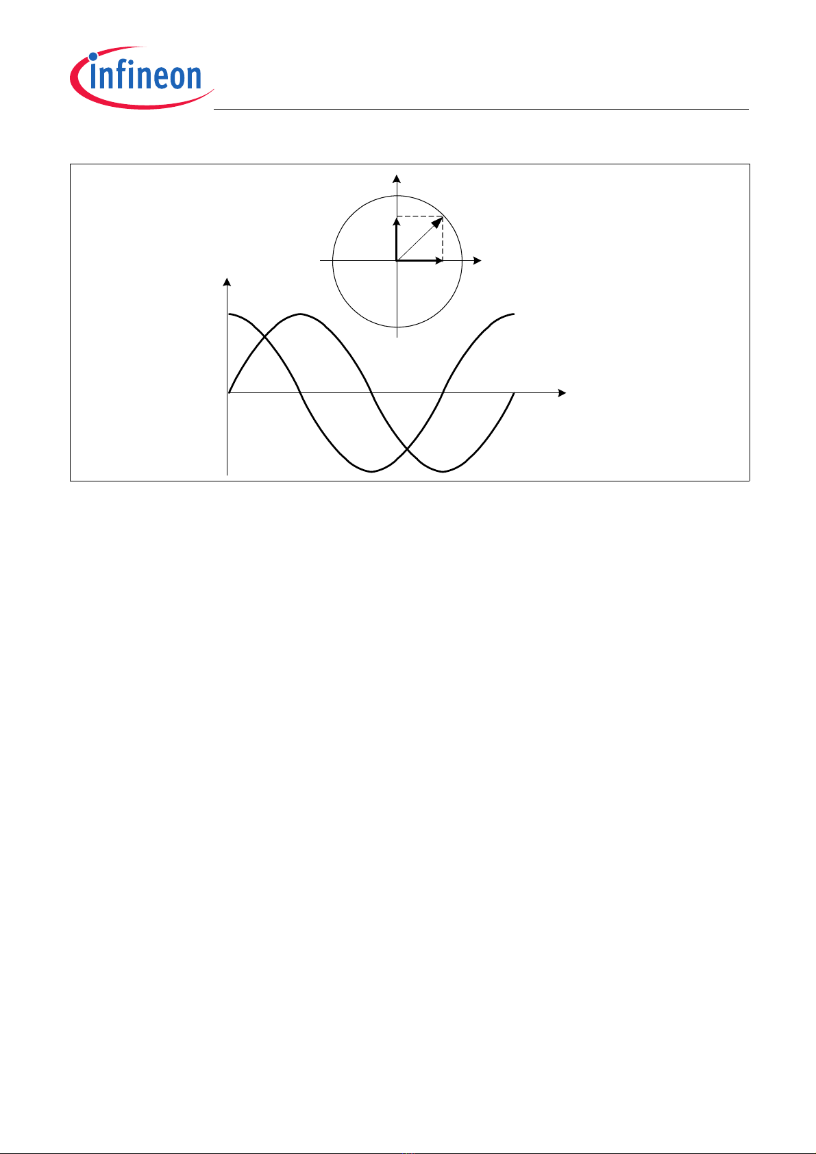
2.3 Sensing Principle
The Giant Magneto Resistance (GMR) sensor is implemented using vertical integration. This means that the
GMR-sensitive areas are integrated above the logic part of the TLE5012B device. These GMR elements change
their resistance depending on the direction of the magnetic field.
Four individual GMR elements are connected to one Wheatstone sensor bridge for each of the two components
of the applied magnetic field:
• X component, Vx(cosine) and the
• Y component, Vy(sine)
With this full-bridge structure the maximum GMR signal is available and temperature effects cancel out each other.
Figure 2-4 Sensitive bridges of the GMR sensor (not to scale)
Attention: Due to the rotational placement inaccuracy of the sensor IC in the package, the sensors 0°
position may deviate by up to 3° from the package edge direction indicated in Figure 2-4.
In Figure 2-4, the arrows in the resistors represent the magnetic direction which is fixed in the Reference Layer.
On top of the Reference Layer, and separated by a non magnetic layer, there is a Free Layer. When applying an
external magnetic field the Free Layer moves in the same direction as the external magnetic field, while the
Reference Layer remains fix. The resistance of the GMR elements depends on the magnetic direction difference
between the Reference Layer and the Free Layer.
When the external magnetic field is parallel to the direction of the Reference Layer, the resistance is minimal
(Reference Layer and Free Layer are parallel). When the external magnetic field and the Reference Layer are anti-
parallel (Reference Layer and Free Layer are anti-parallel), resistance is maximal.
The output signal of each bridge is only unambiguous over 180° between two maxima. Therefore two bridges are
oriented orthogonally to each other to measure 360°.
With the trigonometric function ARCTAN2, the true 360° angle value is calculated out of the raw X and Y signals
from the sensor bridges.
V
DD
GNDADC
X
+
GMR Resistors
ADC
X
-ADC
Y
+ADC
Y
-
V
X
V
Y
0°
N
S
90°
TLE5012B
Functional Description
User’s Manual 15 Rev. 1.2, 2018-02
Figure 2-5 Ideal output of the GMR sensor bridges
V
Angle α
90° 180° 270° 360°0°
V
X
(COS)
Y Component (SIN)
V
Y
(SIN)
V
Y
V
X
X Component (COS)

TLE5012B
Functional Description
User’s Manual 16 Rev. 1.2, 2018-02
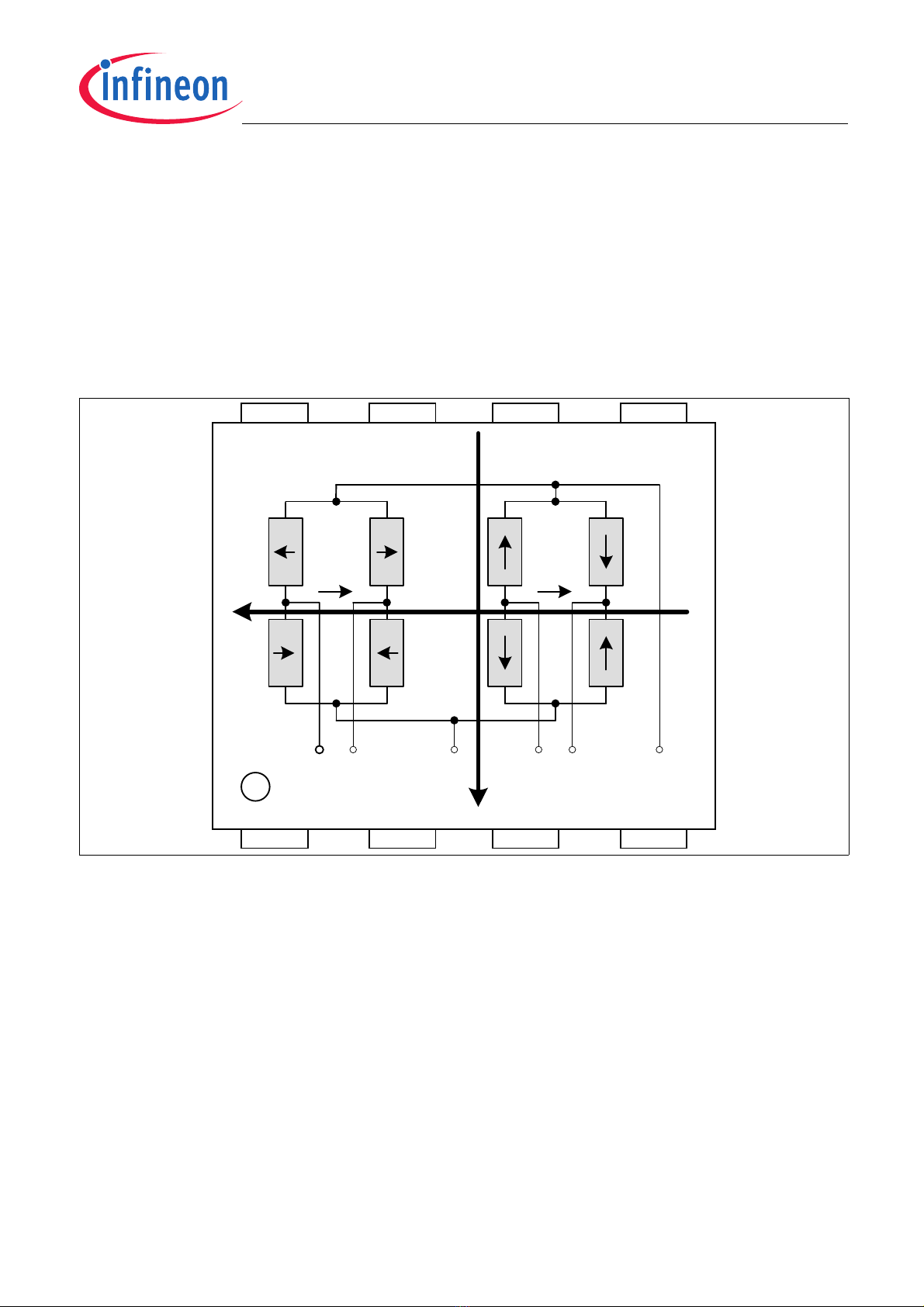
2.4 Pin Configuration
Figure 2-6 Pin configuration (top view)
2.5 Pin Description
Table 2-1 Pin Description
Pin No. Symbol In/Out Function
1IFC
(CLK / IIF_IDX / HS3)
I/O Interface C:
External Clock1) / IIF Index / Hall Switch
Signal 3
1) External clock feature is not available in IIF or HSM interface mode
2 SCK I SSC Clock
3 CSQ I SSC Chip Select
4 DATA I/O SSC Data
5IFA
(IIF_A / HS1 / PWM / SPC)
I/O Interface A:
IIF Phase A / Hall Switch Signal 1 /
PWM / SPC output (input for SPC trigger
only)
6V
DD - Supply Voltage
7GND-Ground
8IFB
(IIF_B / HS2)
O Interface B:
IIF Phase B / Hall Switch Signal 2
12 34
5678 Center of Sensitive
Area
TLE5012B
Application Circuits
User’s Manual 17 Rev. 1.2, 2018-02
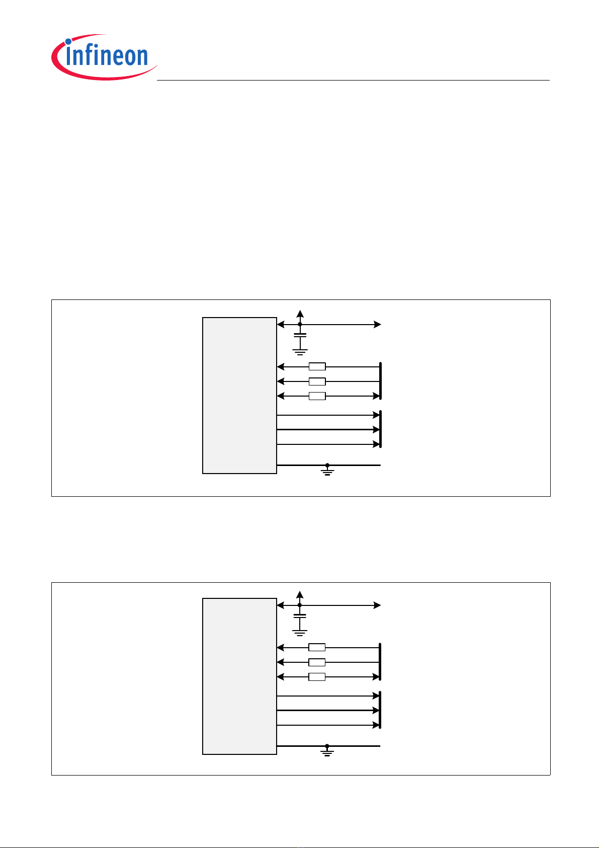
3 Application Circuits
The application circuits in this chapter show the various communication possibilities of the TLE5012B. The pin
output mode configuration is device-specific and it can be either push-pull or open-drain. The bit IFAB_OD
(register IFAB, 0DH) indicates the output mode for the IFA, IFB and IFC pins. The SSC pins are by default push-
pull (bit SSC_OD, register MOD_3, 09H). Every application circuits below are using otherwise specified SSC with
push-pull configuration and the internal clock.
3.1 IIF interface and SSC (IIF in push-pull configuration)
Figure 3-1 shows a block diagram of a TLE5012B with Incremental Interface (IIF) and SSC interface. The derivate
TLE5012B - E1000 is by default configured with push-pull IFA (IIF_A), IFB (IIF_ B) and IFC (IIF_IDX) pins. When
the output pins are configurated as open-drain, three pull-up resistors should be added (e.g. 2k2Ω) between the
data lines and VDD.
Figure 3-1 Application circuit for TLE5012B with IIF interface and SSC
3.2 HSM interface and SSC (HSM in push-pull configuration)
Figure 3-2 shows a block diagram of the TLE5012B with Hall Switch Mode (HSM) and SSC interface. The derivate
TLE5012B - E3005 is by default configurated with push-pull IFA (HS1), IFB (HS2) and IFC (HS3) pins.
Figure 3-2 Application circuit for TLE5012B with HSM interface (push-pull configuration) and SSC
TLE5012B
CSQ
SCK
DATA
IFA
IFB
IFC
GND
VDD
3.0 – 5.5V
Rs1
SSC
IIF
100nF
(IIF_A)
(IIF_B)
(IIF_IDX)
Rs1
Rs2
Rs1 recommended, e.g. 100
Rs2 recommended, e.g. 470
TLE5012B
CSQ
SCK
DATA
IFA
IFB
IFC
GND
VDD
3.0 – 5.5V
Rs1
SSC
HSM
100nF
(HS1)
(HS2)
(HS3)
Rs1
Rs2
Rs1 recommended, e.g. 100
Rs2 recommended, e.g. 470

TLE5012B
Application Circuits
User’s Manual 18 Rev. 1.2, 2018-02
3.3 HSM interface and SSC (HSM in open-drain configuration)
As shown in Figure 3-3 when IFA, IFB and IFC are configurated via the SSC interface as open drain pins, three
pull-up resistors (Rpu) should be added on the output lines.
Figure 3-3 Application circuit for TLE5012B with HSM interface (open-drain configuration) and SSC
3.4 PWM interface (push-pull configuration)
The TLE5012B can be configured with PWM only (Figure 3-4). The derivate TLE5012B - E5000 is by default
configurated with push-pull configuration for IFA (PWM) pin. Internal pull-up resistors are always available for
DATA and CSQ pins (see Datasheet). It is recommended to connect CSQ pin to VDD to provide a high level and
avoid unintentional activation of the SSC interface. DATA pin should be left open. The figure below shows a typical
implementation of the TLE5012B - E5000.
Figure 3-4 Application circuit for TLE5012B with PWM (push-pull configuration) interface
TLE5012B
CSQ
SCK
DATA
IFA
IFB
IFC
GND
VDD
3.0 – 5.5V
Rs1
SSC
HSM
100nF
(HS1)
(HS2)
(HS3)
Rs1
Rs2
Rs1 recommended, e.g. 100
Rs2 recommended, e.g. 470
Rpu
Rpu
Rpu
Rp u requir ed, e.g. 2K2
TLE5012B
CSQ
SCK
DATA
IFA
IFB
IFC
GND
VDD
3.0 – 5.5V
100nF
(PWM)
Rpd recommended, e.g. 10k
PWM

TLE5012B
Application Circuits
User’s Manual 19 Rev. 1.2, 2018-02
3.5 PWM interface (open-drain configuration)
The TLE5012B - E5020 is also a PWM derivate but with open drain for IFA (PWM) pin. A pull-up resistor (e.g.
2.2kΩ) should be added between the IFA line and VDD, as shown in Figure 3-5.
Internal pull-up resistors are always available for DATA and CSQ pins (see Datasheet). It is recommended to
connect CSQ pin to VDD to provide a strong level and avoid unintentional activation of the SSC interface. DATA
pin should be left open. The figure below shows a typical implementation of the TLE5012B - E5020.
Figure 3-5 Application circuit for TLE5012B with PWM (open-drain configuration) interface
3.6 SPC interface
The TLE5012B can be configured with SPC only (Figure 3-6). This is only possible with the TLE5012B - E9000
derivate, which is by default configurated with an open-drain IFA (SPC) pin.
In Figure 3-6 the IFC (S_NR[1]) and SCK (S_NR[0]) pins are set to ground to generate the slave number (S_NR)
0D(or 00B). In case of SCK (S_NR[0]) needs to be set to VDD to generate another slave address, CSQ pin should
be set to ground instead. Internal pull-up resistors are always available for DATA and CSQ pins (see Datasheet).
DATA pin should be left open. Since SCK and CSQ pins should have opposite level, it is not recommended to use
the SSC interface in parallel.
Figure 3-6 Application circuit for TLE5012B with SPC interface
TLE5012B
CSQ
SCK
DATA
IFA
IFB
IFC
GND
VDD
3.0 – 5.5V
100nF
(PWM)
Rpd recommended, e.g. 10k
Rpu required, e.g. 2K2
PWM
Rpu
TLE5012B
CSQ
SCK
DATA
IFA
IFB
IFC
GND
VDD
3.0 – 5.5V
100nF
(SPC)
Rpd recommended, e.g. 10k
Rpu required, e.g. 2K2
SPC
Rpu

TLE5012B
Application Circuits
User’s Manual 20 Rev. 1.2, 2018-02
3.7 SSC interface (push-pull configuration)
In Figure 3-1, Figure 3-2 and Figure 3-3 the SSC interface has the default push-pull configuration (see details in
Figure 3-7). A series resistor on the DATA line is recommended to limit the current in erroneous cases (e.g. the
sensor pushes high and the microcontroller pulls low at the same time or vice versa). Resistors on SCK and CSQ
lines are recommended in case of disturbances or noise.
Figure 3-7 SSC interface with push-pull configuration (high-speed application)
3.8 SSC interface (open-drain configuration)
It is possible to use an open-drain configuration for the DATA line. This setup can be used to communicate with a
microcontroller in a bus system, together with other SSC slaves (e.g. two TLE5012B devices for redundancy
reasons). This mode can be activated using the bit SSC_OD.
Even though, push-pull configuration in a bus system is also possible since the addressing of the sensor is
perfomed with CSQ pin.
The open-drain configuration can be seen in Figure 3-8. Series resistors on the DATA line are recommended to
limit the current in erroneous cases. Resistors on SCK and CSQ lines are recommended in case of disturbances
or noise A pull-up resistor of typ. 1 kΩis required on the DATA line.
Figure 3-8 SSC interface with open-drain configuration (bus systems)
Shift Reg.
Shift Reg.
Clock Gen.
DATA MTSR
MRST
SCK SCK
(SSC Slave) TLE 5012B µC (SSC Master)
CSQ CSQ
EN EN
Rs1 recommended, e.g. 100
Rs2 recommended, e.g. 470
Rs1
Rs1
Rs2
Shift Reg.
Shift Reg.
Clock Gen.
DATA MTSR
MRST
SCK SCK
(SSC Slave) TLE 5012B µC (SSC Master)
CSQ CSQ
Rs1 recommended, e.g. 100
Rpu required, e.g. 1k
Rs1
Rs1
Rs1 Rs1
Rpu
EN
EN
Table of contents


