Infineon S6BT112A User manual

Application Note Please read the Important Notice and Warnings at the end of this document 002-27376 Rev. *A
www.infineon.com page 1 of 19 2021-06-15
AN227376
Getting Started with CXPI Transceiver
S6BT112A
About this document
Scope and purpose
AN227376 introduces you to the Japanese Automotive Standards Organization (JASO) Clock Extension
Peripheral Interface (CXPI)-compliant S6BT112A transceiver chip, which has the unique wave-shaping function
for low Electromagnetic Interference (EMI). This application note describes an example of hardware connection
with the CXPI data link controller (MCU) and the CXPI bus line. In addition, it explains how the data link
controller shifts the operation mode and arbitrates transmission with the CXPI protocol.
Associated Part Family
S6BT112A
Related Documents
S6BT112A Datasheet
Table of contents
About this document....................................................................................................................... 1
Table of contents............................................................................................................................ 1
1CXPI communication protocol ................................................................................................. 3
2S6BT112A CXPI transceiver...................................................................................................... 4
3Hardware configuration.......................................................................................................... 6
3.1 Master node connection example ..........................................................................................................6
3.2 Slave node connection example.............................................................................................................6
4Software configuration........................................................................................................... 8
4.1 Mode transition .......................................................................................................................................8
4.1.1 Mode transition diagram ...................................................................................................................8
4.1.2 Transition from Normal mode to Sleep mode..................................................................................9
4.1.3 Transition from Sleep mode to Normal mode................................................................................10
4.1.3.1 Master node trigger.....................................................................................................................10
4.1.3.2 Slave node trigger.......................................................................................................................11
4.2 Arbitration .............................................................................................................................................13

Application Note 2 of 19 002-27376 Rev. *A
2021-06-15
Getting Started with CXPI Transceiver S6BT112A
CXPI communication protocol
4.3 Baud rate detection period and fail-safe decode initialization...........................................................15
4.3.1 Baud rate detection period..............................................................................................................15
4.3.2 Fail-safe decode initialization..........................................................................................................16
5Glossary...............................................................................................................................17
Revision history.............................................................................................................................18

Application Note 3 of 19 002-27376 Rev. *A
2021-06-15
Getting Started with CXPI Transceiver S6BT112A
CXPI communication protocol
1CXPI communication protocol
CXPI is a communication protocol that consists of three layers: application layer, data link layer, and physical
layer. It has the following features:
•Non-destructive CSMA / CR (carrier sense multiple access/collision resolution) method that ensures high
responsiveness even when many nodes are connected. Similar to Controller Area Network (CAN), the CXPI
protocol provides for event transmission and communication between each node.
•The slave node does not need an external oscillator to extract the data from the bus. It will use the master
clock because the master node sends a clock pulse with data and the slave node synchronizes with the
master clock bit by bit.
•Most general-purpose microcontrollers supports CXPI because it uses UART PHY.
CXPI has the following main features:
•Application layer
−Supports sleep and wakeup
•Data link layer
−Communication through non-destructive type CSMA/CR
−Uses 8 types of error detection including 8-bit /16-bit CRC
−Supports non-destructive mediation of frames
•Physical link layer
−Bus type for network topology
−Single line for communication
−Maximum 16 nodes
−Bus connection length: Maximum 40 m
−Synchronized every PWM bit
−Transfer rate: Maximum 20 kbps

Application Note 4 of 19 002-27376 Rev. *A
2021-06-15
Getting Started with CXPI Transceiver S6BT112A
S6BT112A CXPI transceiver
2S6BT112A CXPI transceiver
The S6BT112A series is a CXPI transceiver that conforms to the JASO CXPI protocol. S6BT112A01 has a built-in
Spread Spectrum Clock Generator (SSCG), while S6BT112A02 has no SSCG. The S6BT112A series has the
following features.
•Operating power supply voltage range: 5.3 V to 18 V
•BUS breakdown voltage: ± 40 V
•ESD breakdown voltage: HBM ± 8 kV
•Support bitrate: 2.4 kbps ~ 20 kbps
The S6BT112A series employs many Cypress-proprietary EMI reduction countermeasure circuits. With these
technologies listed in Table 1, S6BT112A provides the industry’s best low-noise CXPI performance. By
deploying S6BT112A to both the master node and the slave node, significant noise reduction can be obtained.
Table 1 S6BT112A EMI reduction countermeasure circuit
Feature
Measures and effects
Applicable node
Optimal slew rate
control
Harmonics are reduced by lowering the slew rate.
Master / Slave
Optimal control of duty
cycle of the master
clock
By optimally controlling the master clock duty cycle,
harmonics in the keyless frequency band are reduced.
Master
SSCG (Spread
spectrum clock
generator)
The noise peak level is reduced by changing the periodic
frequency of the transceiver’s built-in clock slightly.
Master
Slave bus response
timing optimization
Automatically adjusts the slave to send the LOW pulse too
early or too late to reduce current noise (inductive noise). It
also reduces the noise of the keyless band.
Slave
Figure 1 shows a block diagram of the S6BT112A CXPI transceiver. Table 2 shows the pin functions.
Figure 1 S6BT112A block diagram

Application Note 5 of 19 002-27376 Rev. *A
2021-06-15
Getting Started with CXPI Transceiver S6BT112A
S6BT112A CXPI transceiver
Table 2 S6BT112A pin functions
Pin
Pin name
I/O
Function
1
RXD
O
Receive UART data output pin
2
NSLP
I
Sleep control pin
‘0’: Sleep mode
‘1’: Normal mode / standby mode
3
CLK
I
For master node (SELMS = ‘0’): Baud rate clock input pin
O
Slave node (SELMS = ‘1’): Baud rate clock output pin
NSLP = HIGH: Decoding BUS clock output
NSLP = LOW: Bus clock output without decoding
4
TXD
I
Transmit UART data input pin
5
GND
–
Ground pin
6
BUS
I/O
Bus line input / output pin
7
BAT
–
Battery power input pin
8
SELMS
I
Master / slave switching pin
‘0’: Master
‘1’: Slave

Application Note 6 of 19 002-27376 Rev. *A
2021-06-15
Getting Started with CXPI Transceiver S6BT112A
Hardware configuration
3Hardware configuration
3.1 Master node connection example
When using S6BT112A as a master node, pull down the master / slave switching pin (SELMS: 8 pin). The baud
rate clock, generated by the master node using the MCU timer, is the input to the clock input pin (CLK: 3 pin).
Note that, the MCU UART baud rate and timer output need not be synchronized. The TXD and RXD pins are
connected to the MCU's UART pin, and the BUS pin is pulled up to VBATTERY with a 1-kΩ resistor. The NSLP pin
controls the S6BT112A mode transition between the Sleep mode and the Normal mode after power-on with the
GPIO of the MCU.
Figure 2 shows the master node circuit connection (example using Traveo II MCU).
220 pF
+5 V or +3.3 V
S6BT112A
RXD
NSLP
CLK
TXD
SELMS
BAT
BUS
GND
1
2
3
4
8
7
6
5
GND
+B
BUS
GND
GND
GND
GND
10 kΩ
10 µF
10 kΩ
0.1 µF
GND
CYT2B9
VDDD
GND
P20-5/
CXPI3_RX
P12-5/
GPIO
P14-6/
PWM
P20-6/
CXPI3_TX
R4
R3
D1
GND R6
1N4148
D3
1 kΩ
TVII R2
10 kΩ
Figure 2 Example of master node connection consisting of Traveo II MCU and S6BT112A
3.2 Slave node connection example
When using S6BT112A as a slave node, pull up the master / slave switching pin (SELMS: 8 pin). The clock output
pin (CLK: 3 pin) is connected to the MCU external interrupt pin, GPIO input pin, etc. It is used to detect the
wakeup pulse in the Sleep mode, or to measure the communication baud rate in the Normal mode and the
baud rate on the MCU side. Connect the TXD and RXD pins to the MCU's UART pin. The NSLP pin controls the
S6BT112A mode transition between the Sleep mode and the Normal mode after power on with the GPIO of the
MCU.

Application Note 7 of 19 002-27376 Rev. *A
2021-06-15
Getting Started with CXPI Transceiver S6BT112A
Hardware configuration
Figure 3 shows circuit connection of slave nodes (this example uses PSoC 4).
220 pF
+5 V or +3.3 V
S6BT112A
RXD
NSLP
CLK
TXD
SELMS
BAT
BUS
GND
1
2
3
4
8
7
6
5
GND
R3 +B
BUS
GND
GND
GND
GND
10 kΩ
10 µF
10 kΩ
0.1 µF
GND
PSoC4100S
Plus
VDD
GND
P1.0/
uart_rx
P0.1/
in_n
P3.0/
io
P1.1/
uart_tx
R4
R2
10 kΩ
D1
Figure 3 Connection example of slave node configured with PSoC 4 and S6BT112A
In case of adding the secondary clock master operation, the SELMS pin must be connected to the GPIO of the
MCU in addition to being pulled up. When switching to the secondary clock master operation in the power on
state, make sure that the NSLP pin is set to LOW and transition to the Sleep mode, and after confirming that
there is no communication such as Wakeup pulse on the BUS at the CLK pin, switch the SELMS pin to LOW.
Input the baud rate clock to the CLK pin.

Application Note 8 of 19 002-27376 Rev. *A
2021-06-15
Getting Started with CXPI Transceiver S6BT112A
Software configuration
4Software configuration
4.1 Mode transition
4.1.1 Mode transition diagram
Figure 4 shows the mode transition diagram of S6BT112A.
Figure 4 Mode transition diagram of S6BT112A
S6BT112A mainly has the following three operating modes:
•Sleep mode
•Standby mode
•Normal mode

Application Note 9 of 19 002-27376 Rev. *A
2021-06-15
Getting Started with CXPI Transceiver S6BT112A
Software configuration
By controlling the NSLP pin, it is possible to transition between the three modes. To suppress the power
consumption of nodes that are constantly supplied with power, it is possible to transition to the power-saving
Sleep mode. In systems where power is supplied only when needed, you can choose not to use the
Wakeup/Sleep function.
Sleep mode is a power-saving mode in which each node stops sending and receiving data. All nodes transition
to Sleep mode after the power is turned on. Ensure that you turn on the power with NSLP = LOW. During Sleep
mode, the BUS signal is received without being decoded, and will be transmitted out from the RXD terminal at
the master node and from the CLK terminal at the slave node.
Standby mode is a transient mode during the transition from Sleep mode to Normal mode. During Standby
mode, transmission and reception output are suspended. When setting NSLP to HIGH, S6BT112A first
transitions to Standby mode. After the TMODE_CHG time, S6BT112A transitions to Normal mode automatically.
Normal mode is a mode in which communication is possible. During Normal mode, the transmission data,
which is input to the TXD terminal is encoded and output to the BUS line. The received BUS data is decoded
and output to the RXD terminal.
In addition to the operating modes, there are ThermalShutdown mode and WP_ThermalShutdown mode as
failsafe functions to prevent malfunctions at abnormally high device temperature. In Thermal Shutdown mode,
the clock or data from the MCU to the BUS will be stopped, but the decoded BUS signal can be monitored by
the output of the CLK terminal or RXD terminal. In WP_ThermalShutdown mode, the non-decoded BUS signal
can be monitored by the output of CLK terminal. When the temperature falls to the normal range, S6BT112A
transitions from WP_ThermalShutdown mode to Sleep mode.
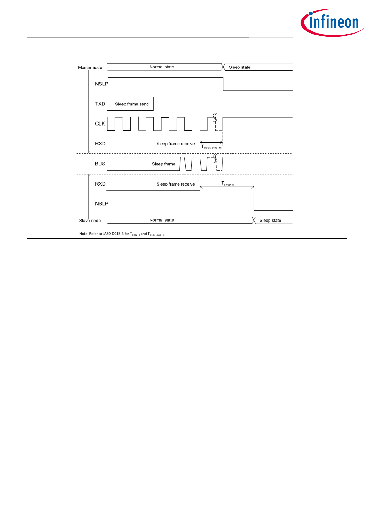
4.1.2 Transition from Normal mode to Sleep mode
When the Sleep condition is met, the master node can transmit a Sleep frame.
The master node stops the clock output at Tclock_stop_m time after receiving the Sleep frame. When the slave node
receives the Sleep frame, it prepares for Sleep and sleeps at Tsleep_s time (see JASO D015-3 for Tclock_stop_m time
and Tsleep_s time).
S6BT112A transitions to Sleep mode by changing the NSLP pin from HIGH to LOW. Set the master node CLK pin
to HIGH in Sleep mode. Also, set the TXD pin to HIGH when not communicating according to the UART protocol.
The transition flow chart and timing chart from Normal mode to Sleep mode are shown in Figure 5 and
Figure 6 respectively.
Figure 5 Transition flow from Normal mode to Sleep mode
Application Note 10 of 19 002-27376 Rev. *A
2021-06-15
Getting Started with CXPI Transceiver S6BT112A
Software configuration
Figure 6 Transition timing from Normal mode to Sleep mode
4.1.3 Transition from Sleep mode to Normal mode
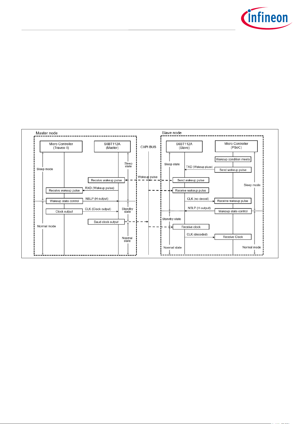
4.1.3.1 Master node trigger
When the master node detects an internal factor event such as sensor detection in Sleep mode, it sets the NSLP
pin of S6BT112A to HIGH to transition back to Normal mode. In addition, the master node will transmit the
baud rate clock to the transceiver CLK pin to transmit the clock to the communication bus.
In the slave node, when S6BT112A receives the BUS clock, it outputs the non-decoded clock signal from the CLK
terminal. With that as a trigger, the MCU sets the NSLP pin of S6BT112A to HIGH within Twakeup_s time to
transition to Standby mode. Upon receiving the clock from the bus, and the slave node will transition to Normal
mode (see JASO D015-3 for Twakeup_s time) from standby mode.

Application Note 11 of 19 002-27376 Rev. *A
2021-06-15
Getting Started with CXPI Transceiver S6BT112A
Software configuration
The transition flow chart and timing chart from Sleep Mode to Normal Mode (Master Node Trigger) are shown in
Figure 7 and Figure 8 respectively.
Figure 7 Transition flow from Sleep mode to Normal mode (Master node trigger)
Figure 8 Transition timing from Sleep mode to Normal mode (Master node trigger)
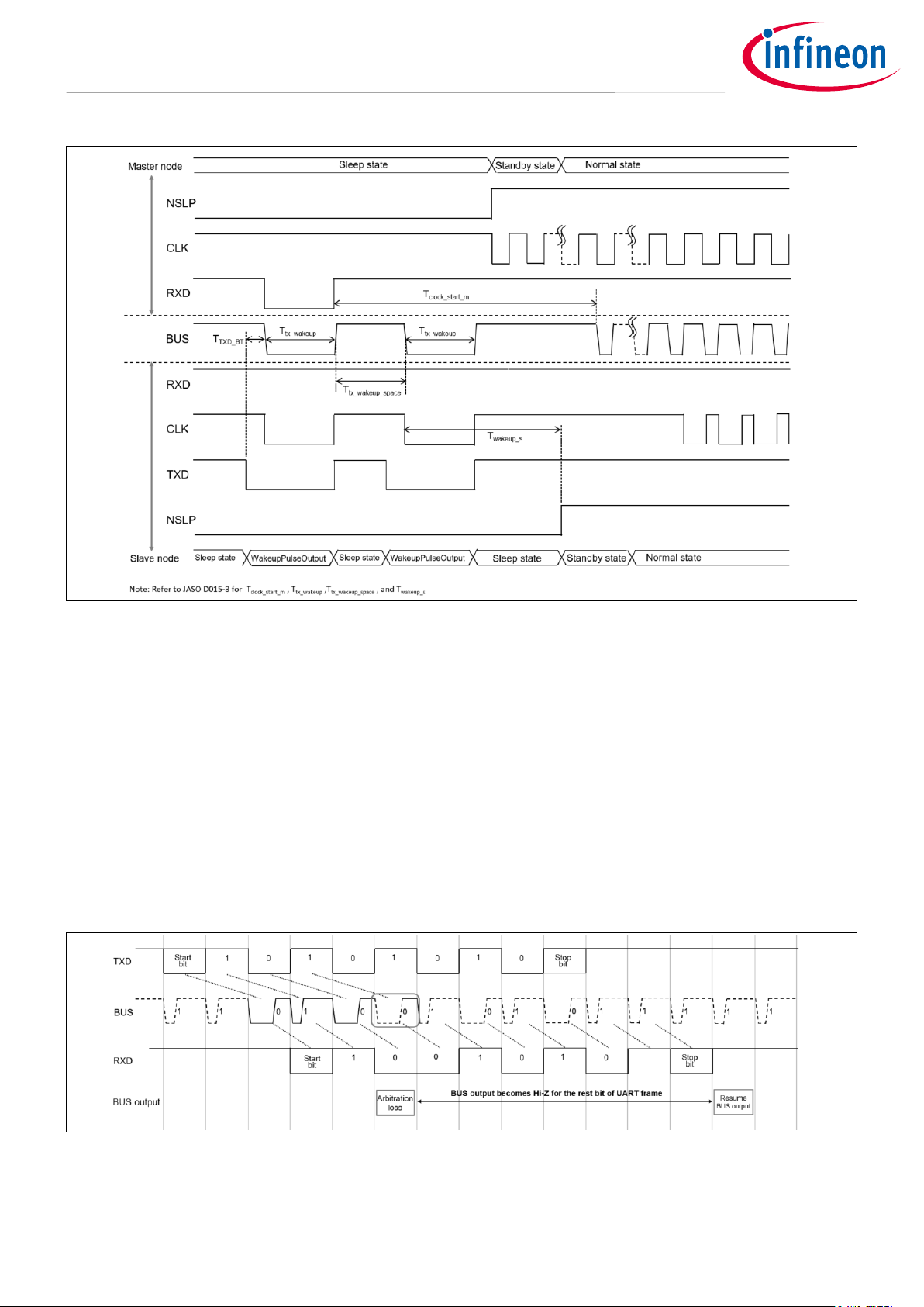
4.1.3.2 Slave node trigger
After detecting an internal wakeup event, the slave node sends a Wakeup pulse to the communication bus via
the TXD pin.
In the master node, when S6BT112A receives the BUS wakeup pulse, it transmits the non-decoded wakeup
pulse to the RXD terminal. In response to this, the MCU sets NSLP pin to HIGH within Tclock_start_m time to
transition to Normal mode, and then the master node will start transmitting the baud rate clock to the CLK pin
to transmit the clock to the communication bus.
Application Note 12 of 19 002-27376 Rev. *A
2021-06-15
Getting Started with CXPI Transceiver S6BT112A
Software configuration
On the other hand, in the slave node, the non-decoded BUS wakeup pulse is output to the CLK terminal. In
response to this, the slave node sets the NSLP pin to HIGH to transition to the Normal mode within Twakeup_s time.
If the slave node cannot receive the bus clock within the specified time after sending the Wakeup pulse, it will
set the NSLP pin to LOW to return to Sleep mode. Then, the Wakeup pulse can be retransmitted. A slave node
can transmit a Wakeup pulse for maximum of two times, including retransmission of the Wakeup pulse. If the
clock is not transmitted from the master node even after retransmission, the wakeup sequence can be
performed again after Sleep in physical bus error processing. (See JASO D015-3 for Tclock_start_m time and Twakeup_s
time).
The transition flow chart and timing chart from Sleep Mode to Normal Mode (Slave Node Trigger) are shown in
Figure 9 and Figure 10 respectively.
Figure 9 Transition flow from Sleep mode to Normal mode (Slave node trigger)
Application Note 13 of 19 002-27376 Rev. *A
2021-06-15
Getting Started with CXPI Transceiver S6BT112A
Software configuration
Figure 10 Transition timing from Sleep mode to Normal mode (Slave node trigger)
4.2 Arbitration
The arbitration function of the CXPI protocol is implemented by using the MCU and transceiver.
Bitwise arbitration within the UART frame is performed on the transceiver side, and bytewise arbitration
between UART frames is performed on the MCU side.
Figure 11 shows the timing chart of S6BT112A bitwise arbitration.
When PID transmission is in Normal mode, S6BT112A compares the transmitted bit with the bit received from
the CXPI BUS. If they match, the BUS output continues. If they do not match, it means that the node lost the
arbitration; the BUS output of S6BT112A becomes High-Z to cancel the transmission of the remaining PID bits.
Even if the node lost the arbitration, it continues data reception from the BUS.
Figure 11 S6BT112A arbitration function timing

Application Note 14 of 19 002-27376 Rev. *A
2021-06-15
Getting Started with CXPI Transceiver S6BT112A
Software configuration
On the other hand, the MCU side compares the transmission byte (TXD) and the reception byte (RXD). If they do
not match, it means that the node lost the arbitration, and the MCU stops transmission of the remaining frame
data. The next PID transmission is delayed until IFS is detected. (Refer to JASO D015-3 for detail)
Figure 12 shows an example of MCU arbitration function processing.
As described in the S6BT112A datasheet, S6BT112A has transmission / reception delay. To implement the
arbitration function correctly, ensure that you implement the following two functions on the MCU side:
1. Check whether UART reception is in progress before transmission.
2. Verify the transmitted data and received data after the transmission.
There are two ways to check whether UART reception is in progress.
1. Use the MCU’s UART peripheral status function.
2. Use the MCU’s GPIO interrupt function.
Select the method according to the MCU to be used. When using Method 2, ensure that the MCU is fully meets
the requirements, taking the noise into account.
Figure 12 MCU arbitration function processing example

Application Note 15 of 19 002-27376 Rev. *A
2021-06-15
Getting Started with CXPI Transceiver S6BT112A
Software configuration
4.3 Baud rate detection period and fail-safe decode initialization
4.3.1 Baud rate detection period
After power-on, when the NSLP pin is set to HIGH to transition to Normal mode, S6BT112A detects the clock
cycle and initializes the LOW width of logical value ‘1’. Data cannot be transmitted or received during the 33 Tbit
clock cycle detection period.
In the master node, S6BT112A starts to output the clock to BUS with an optimized duty cycle after 33 CLK
clocks. In the slave node, S6BT112A starts to output the decoded clock based on the initialized LOW width of
logical value ‘1’to the CLK terminal after 33 BUS clocks.
The timing chart of baud rate detection period at power on is shown in Figure 13.
Figure 13 Baud rate detection timing (At power ON)
After transitioning from Normal mode to Sleep mode with the power on, the NSLP pin is set to HIGH again to
transition to Normal mode. Data transmission and reception is available after transition from Standby mode to
Normal mode, using the clock cycle and the LOW width of logical value ‘1’ detected in the previous Normal
mode.
In the master node, when S6BT112A transitions to Normal mode, it starts to transmit the clock to BUS with an
optimized duty cycle. In the slave node, when S6BT112A transitions to Normal mode, S6BT112A starts to output
the decoded clock to the CLK terminal, based on the recorded LOW width of the logical value ‘1’.
The timing chart of baud rate detection period while continuous power is shown in Figure 14.
Figure 14 Baud rate detection timing (Continuous power supply)

Application Note 16 of 19 002-27376 Rev. *A
2021-06-15
Getting Started with CXPI Transceiver S6BT112A
Software configuration
4.3.2 Fail-safe decode initialization
During the Normal mode in slave node, when a BUS clock pulse with abnormally short LOW width is received
due to the influence of noise, the subsequent clock is erroneously determined as a logical value ‘0’. If 10 logical
‘0’values are received continuously, S6BT112A automatically initializes the decoding process to return to
normal operation. External initialization processing is not necessary.
The fail-safe decode initialization timing chart is shown in Figure 15.
Figure 15 Fail-safe decode initialization timing

Application Note 17 of 19 002-27376 Rev. *A
2021-06-15
Getting Started with CXPI Transceiver S6BT112A
Glossary
5Glossary
Table 3 Glossary
Terms
Description
CR
Collision Resolution
CRC
Cyclic Redundancy Check
CSMA
Carrier Sense Multiple Access
CXPI
Clock Extension Peripheral Interface
IBS
Inter Byte Space
IFS
Inter Frame Space
PID
Protected Identifier
PWM
Pulse Width Modulation

Application Note 18 of 19 002-27376 Rev. *A
2021-06-15
Getting Started with CXPI Transceiver S6BT112A
Revision history
Revision history
Document
version
Date of release
Description of changes
**
2019-10-11
New application note.
*A
2021-06-15
Updated to Infineon template.

Trademarks
All referenced product or service names and trademarks are the property of their respective owners.
Edition 2021-06-15
Published by
Infineon Technologies AG
81726 Munich, Germany
© 2021 Infineon Technologies AG.
All Rights Reserved.
Do you have a question about this
document?
Go to www.cypress.com/support
Document reference
002-27376 Rev. *A
IMPORTANT NOTICE
The information contained in this application note is
given as a hint for the implementation of the
product only and shall in no event be regarded as a
description or warranty of a certain functionality,
condition or quality of the product. Before
implementation of the product, the recipient of this
application note must verify any function and other
technical information given herein in the real
application. Infineon Technologies hereby disclaims
any and all warranties and liabilities of any kind
(including without limitation warranties of non-
infringement of intellectual property rights of any
third party) with respect to any and all information
given in this application note.
The data contained in this document is exclusively
intended for technically trained staff. It is the
responsibility of customer’s technical departments
to evaluate the suitability of the product for the
intended application and the completeness of the
product information given in this document with
respect to such application.
For further information on the product, technology,
delivery terms and conditions and prices please
contact your nearest Infineon Technologies office
(www.infineon.com).
WARNINGS
Due to technical requirements products may
contain dangerous substances. For information on
the types in question please contact your nearest
Infineon Technologies office.
Except as otherwise explicitly approved by Infineon
Technologies in a written document signed by
authorized representatives of Infineon
Technologies, Infineon Technologies’ products may
not be used in any applicationswhere a failure of the
product or any consequences of the use thereof can
reasonably be expected to result in personal injury.
Table of contents
Other Infineon Transceiver manuals

Popular Transceiver manuals by other brands


Art
Art Flystick3 quick guide

Nokia
Nokia NSE-5 Series Disassembly instructions

Toshiba
Toshiba TC32306FTG manual

QRP Labs
QRP Labs QCX Troubleshooting

Technisonic Industries Limited
Technisonic Industries Limited TFM-138 Operator's guide

Shenzhen ATC Technology
Shenzhen ATC Technology GD230V-8 instruction manual


