Jeds Peds TS808 MAX User manual


Page3
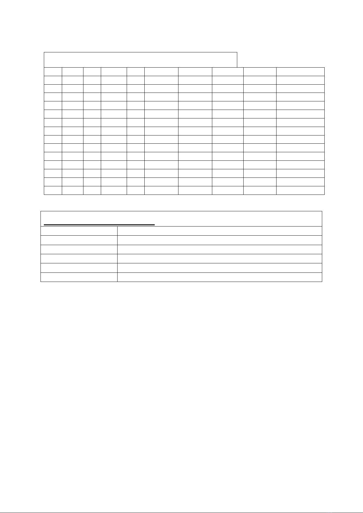
Parts List –Main Circuit
R1
1M
R16
470K
C1
EMPTY
C16
1U
FAT
SPDT O/F/O
R2
1K
R17
10K
C2
47N
C17
EMPTY
CLIP
SPDT O/F/O
R3
470K
R18
100R
C3
68N
C18
220N
DRV
500KA
R4
4K7
R19
10K
C4
22N
TONE
20KB
R5
10K
R20
EMPTY
C5
47N
U1
4558
VOL
100KA
R6
47K
R21
1K
C6
EMPTY
Q1+4
5088
R7
10K
C7
1U
D1,7,4,8
BAT41
JUMPERS
JP1, JP3, JP5
R8
1K
C8
100P
Q2+3
2N7000
R9
10K
C9
EMPTY
D5,6,11
4148
R10
220R
C10
220N
D10
JUMPER
R11
47R
C11
47U
D2+3
LED
R12
1K
C12
100N
D9
4001
R13
1K
C13
1U
R14
10K
C14
10U
R15
10K
C15
100N
Offboard Components
3PDT footswitch
Wire
LED
Coloured
Mono Jacks x2
Power Socket 2.1mm
3PDT Footswitch PCB
Supplied when stocked
Please check the kit against the parts list upon receipt, I hand pick kits to order and I am only human.
I appreciate the photograph of my build is clear-ish, but I advise against simply copying it to yours as
components change appearance regularly and this is a multi PCB so there is a very slim chance the
pic is accurate. Please work from the parts list to avoid error.
Some values may be substituted for as near as, there will be little to no difference if you sub a
resistor or capacitor but if you have received a different chip or transistor than shown and cannot
establish if it is an intentional sub, please contact us. A good search term for this would be “is xxxx
an appropriate substitute for xxxx’
Page4
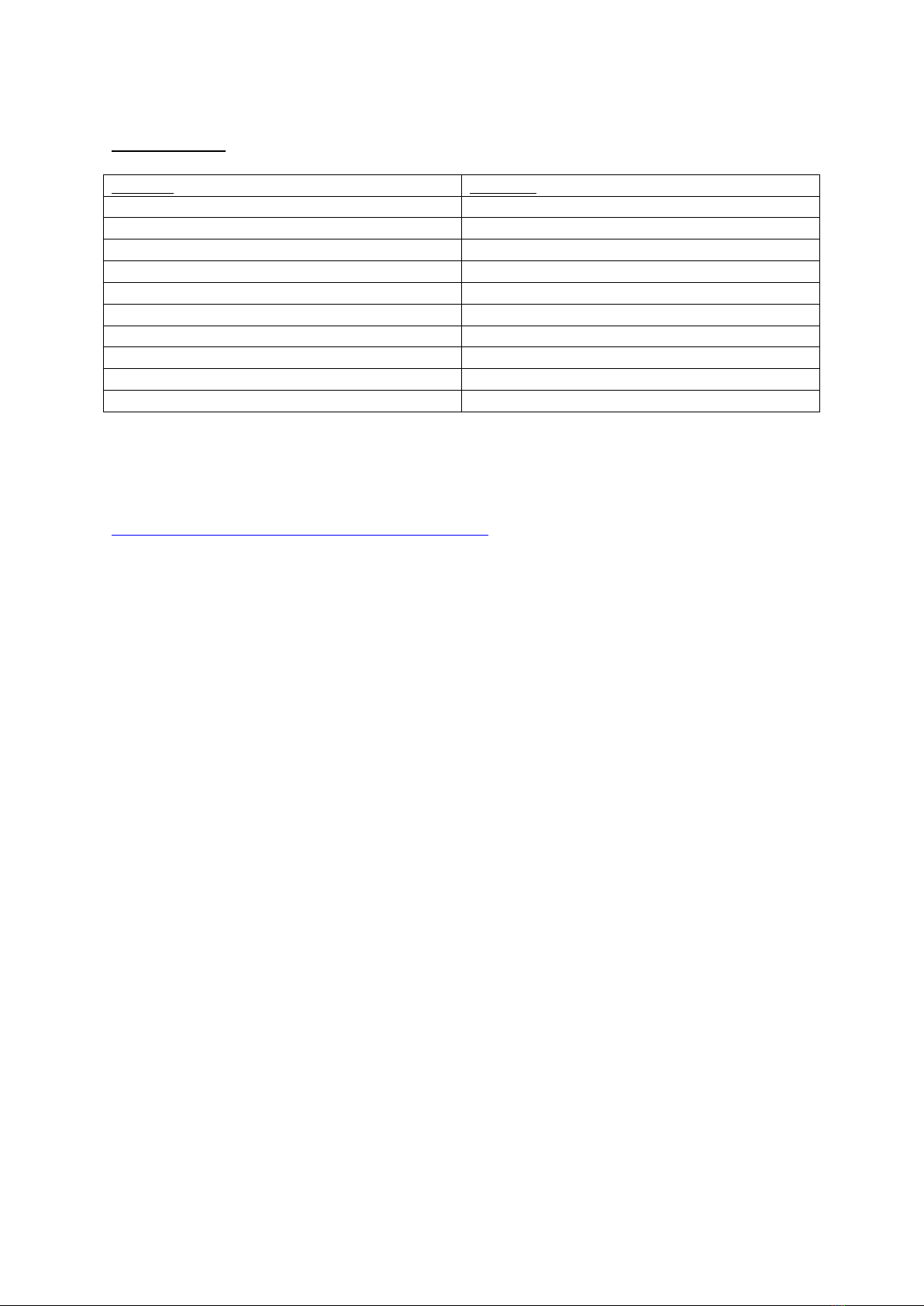
Suggested Tools
Essential
Desirable
Soldering station
Solder - 60/40 or good quality lead free
Wire snipping pliers
Wire stripping pliers
Solder sucker / de solder braid
PCB Clamp
Multi Meter
Centre Punch
Drill bits
Tweezers
The essential tools are all the bare minimum of what I use to build a pedal. The list is not exhaustive,
but we do get a lot of enquiries about what tools people need.
I sell a large range of pedal building related tools here.
Page5
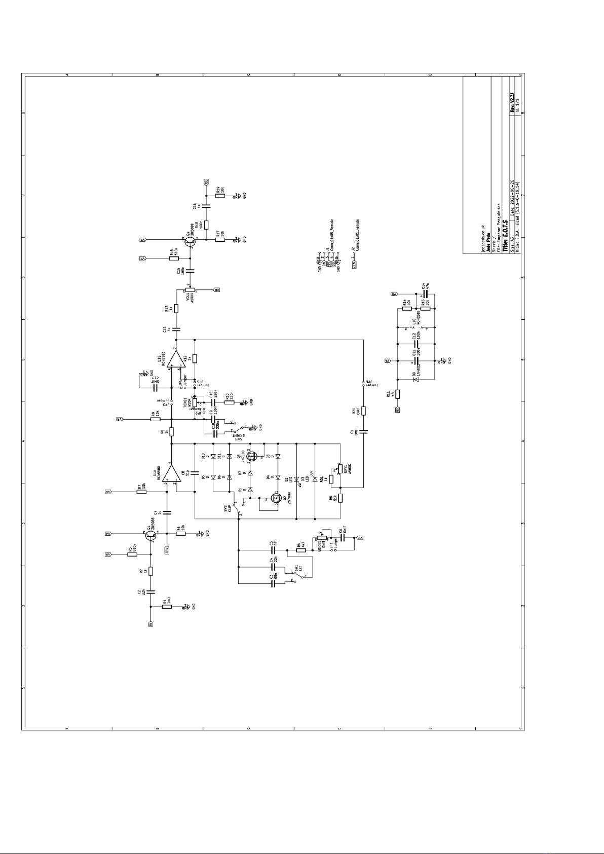
The values above are for a simple TS808, use the values in the BOM
This manual suits for next models
1
Other Jeds Peds Music Pedal manuals


