Jeds Peds More! More! Moore! FV1 User manual


Page3
Parts List –Main Circuit
R1.
1M
SW1
ON ON
C1
100N
U1
TL072
R2.
100K
SW2
ON ON
C3
1U
U2
L78L33
R3.
1K
SW3
ON ON
C4
1N
U3
24LC32
R4.
100K
C6
10U
U4
FV1
R5.
10K
C7
15P
R7.
100R
C8
1U
D1
4001
R8.
100K
C9
1U
D2.3.4
3MM LED
R9.
47K
C11
2N2
R11.
100R
C12
220N
CHORUS
100KB
R13.
10K
C13
470P
REVERB
100KB
R14.
10K
C14
1U
BOOST
100KB
R15.
10K
C15
100U
R16.
10K
C16
47U
Y1
CRYSTAL
R17.
4K7
C17
47U
R18.
4K7
R19.
4K7
R20.
1K
Offboard Components
3PDT footswitch
Wire
LED
Coloured
Mono Jacks x2
Power Socket 2.1mm
3PDT Footswitch PCB
Supplied when stocked
4k7 Resistor
Current Limiting Resistor for the LED –can be up to 10k
Please check the kit against the parts list upon receipt, I hand pick kits to order and I am only human.
I appreciate the photograph of my build is clear-ish, but I advise against simply copying it to yours as
components change appearance regularly. Please work from the parts list to avoid error.
Some values may be substituted for as near as, there will be little to no difference if you sub a
resistor or capacitor but if you have received a different chip or transistor than shown and cannot
establish if it is an intentional sub, please contact us. A good search term for this would be “is xxxx
an appropriate substitute for xxxx’

Page4
Suggested Tools
Essential
Desirable
Soldering station
Solder - 60/40 or good quality lead free
Wire snipping pliers
Wire stripping pliers
Solder sucker / de solder braid
PCB Clamp
Multi Meter
Centre Punch
Drill bits
Tweezers
The essential tools are all the bare minimum of what I use to build a pedal. The list is not exhaustive,
but we do get a lot of enquiries about what tools people need.
I sell a large range of pedal building related tools here.
As the FV1 is a surface mounted component, this video may be of use to you


Page6
A Detailed Overview of the Components in this Kit
Resistors
If we use the analogy of water rather than electricity, then resistors would be called restrictors. They
restrict the flow. Resistors are non-polarised (they can be inserted either way round). The body of a
resistor can be one of many colours. Most commonly seen in our kits are blue or buff.
What really matters is the colour of the bands around the body. There may be 4 or 5 of these. on a
4 band resistor the first two colours give you the value for the resistor and the 3rd gives you the
number of zeros to add (aka the multiplier). With a 5 band resistor the first three give you the value
and the 4th gives you the zeros. See the table below.
So the 4 band resistor above that has rings of green, blue, yellow and gold is a 560000Ω (or 560kΩ).
You will see this ‘value plus zeros’ reappear when we get to capacitors. Note that a 4.7kΩ resistor
would normally be written by me as 4k7.
Note that if the multiplier is gold or silver you divide the leading figures by 10 or 100.
You can either decode them yourself following the above table, alternatively this online resistor
calculator or you can use a multi meter. If you want any further explanation about how to decode
resistor values, this video may help.
There’s also a lovely table below to use as a starting point. NB, whilst most values I use are shown
there is a chance not all will be.

Page7
1% resistors tend to have blue bodies. 5% buff.

Page8
Diodes
Again, going back to the water analogy, diodes can be thought of as one-way valves. They allow
electricity to flow in only one direction. The electrical symbol for a diode is shown below. They must
be inserted in the correct direction for the circuit to work.
The anode is the positive end and the cathode is the
negative. electricity will only flow from the anode to the
cathode. Diodes can be various colours but usually have one
or sometimes two bands at one end.
In this kit you should have 1 diode. The symbol on the PCB will be
something like this, simply line up the band on the diode with the
line on the board.
The diodes in this kit should look like this;
They are fragile, so be careful when you bend the legs.
Diodes, like all silicon components, are heat sensitive. When soldering, limit the contact time as
much as possible. Aim for a maximum of 4 seconds. Less is good! If you have more than one diode
to solder it is good practice to do one leg on each then go back for the second. This way the diode
has time to cool between each leg being soldered.
1N4001

Page9
LED’s
These perform like other diodes except that the glow when a current passes through them.
Their position on the PCB will be shown like this
The LED will also have a flat side.
Generally, the rule would be to match the two and most of the time that is what you will do.
However, to save you de soldering your LED’s I recommend testing them with a multi meter (set to
diode test mode) to be 100% sure you are connecting the positive side where it needs to be. On the
example above the positive feed goes into the round side.
I have come across LED’s orientated opposite to what I expected previously, after installation… so
this quick test is sensible and is one less thing to debug later on. Check twice…solder once.
There are three 3mm leds which mount to the main pcb. I highly recommend that these are added
after everything else, so after the pots and toggle when we get to that stage.
They are quite fiddly to add, and fit to the case, so take your time and remember to keep taking
deep breaths! Its probably easier to solder them one they are through their respective hole, giving
yourself plenty of freedom with adjustments.
The Crystal
The crystal will look like this. A small silver
cylinder with two legs. It is non polarised
which means it does not matter which leg goes
in which hole.
Page10
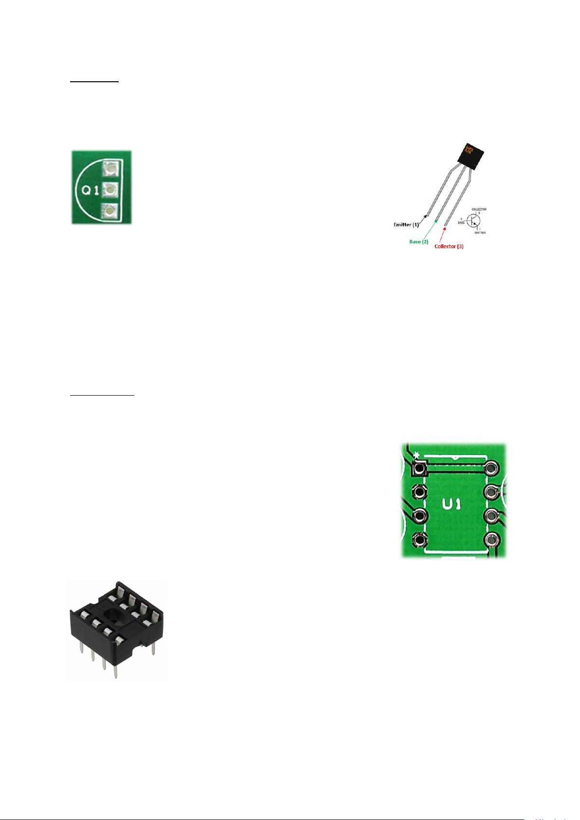
Transistors
This kit comes with transistors
The body of the transistor is usually a small black ‘can’ with a flat on one side.
The shape on the PCB corresponds to the ‘can’
The transistor can be the one listed or any other suitable substitute with matching pin out. The
orientation of this part is crucial. The silkscreen layer indicates which way around it needs to be with
its transistor shaped outline, matching the transistors case. Solder this very carefully.
The same warning about heat when soldering diodes also applies to transistors. Take your time
not to overheat.
The transistor in this kit is a voltage regulator.
IC’s aka ‘chips’
IC’s are small packages that contain many components. The ones that you will find in this kit will
have 8, or 16 legs.
On the PCB pin 1 will be marked with a * and there will be a small notch
drawn on the footprint. The solder pad for pin 1 will be square. The
socket will also have a notch. Be careful with the pins, they are fragile.
This is a socket. I do try to supply sockets for the chips, so unless I am
out of stock you should have one per chip. Solder these in place without
the chip, totally protecting the chip from heat. Please check you have all
pins through the pads before you begin soldering the socket.

Page11
The FV1 is a surface mounted chip. The chip itself has a small dot on
top indicating its pin1. You can see it on this image here, pin1 points to
SW1, and is identified on the silkscreen layer of the PCB with a line
above it.
You can make out the line on the image as well.
Switches
This kit includes 3x DPDT toggle switches.
In this circuit they turn on each individual effect.
The switch can go either way round, in this case the correct connection
of the center pin is essential with the outside lugs able to be used for
either side.
DPDT stands for ‘double pole double throw’. This is
simply 2 SPDT’s in the same package. There are on/on,
on/off/on & on/on/on options and you can place this
either way round.
Capacitors
Capacitors come in many shapes and sizes but fall into two basic camps. Polarised or non polarised.
Capacitors can store energy. For a really good explanation of how they work try this video starting
at 4:25.
This kit uses some non polarised capacitors. The good news is that just like resistors you can insert
them into the PCB either way round.
Now the bad news. they come in a variety of shapes and sizes and although there are supposed to
be standards for markings they do vary. So, what do they look like? This kit predominantly contains
box caps, like this one.

Page12
Now, the marking. Capacitance is measured in Farads (f). 1f is a huge
capacitor. Going down in order there are Millifarads, mf (rarely used) 1
mf is 1/1000th of 1f. Microfarads uf 1/1000th of 1mf. Nanofarads nf
1/1000th of 1uf and Picofarads 1/1000th of 1nf.
Another way to put it is that there are 1000pf in 1nf and 1000nf in 1uf.
Polyester box capacitors with values of 1nf but less than 100nf will have
the value written on the top, either in a very obvious way, or a code.
The capacitor shown above has a value of 100nf. A 1uf capacitor would begin with 1***, value of
1000, so with the additional decimal point, .1k is 100nf. The K is the tolerance (10%) and 63 is the
max voltage. Manufacturers do have other ways of indicating values though unfortunately.
Where things can get difficult is with poly boxes of 100nf and above. sometimes you will see a 100nf
marked as 104xxxx ie the picofarad notation has been used for the value. Equally you may see .1xxxx
ie 0.1uf (the x’s denote the tolerance and voltage). It is still the same 100nf capacitor. The reason
for this is that only 3 digits can be used for the value so 100n cannot be used and 100 would denote
100pf. Still with me? this continues for high values until we get to 1uf which will be marked as
1uxxxx.
Sometimes I supply 1UF MLCC style capacitors marked as 105. These are a small yellow bead. The
different styles of non polarised caps are all interchangeable so do not worry if you expect a box cap
and get a MLCC or vice versa.
Eventually these capacitor and resistor codes will start to sink in! Trust me.
Now onto polarised, they are the simplest. The most common that you
will see are ‘electrolytic’ capacitors. These look like a small beer can
with two protruding wires, usually from the same end, sometimes one
from each end. on the outside of the can will be the value and the max
voltage. Polarised capacitors can only be inserted into the board in one
direction. The PCB will have a + next to the positive terminal.
On the capacitor you will see that one side of the can is marked with
a stripe usually containing negative symbols. The wire nearest to
this is the negative wire. You will also notice that the positive wire is
longer.

Page13
So now it’s time to get down to building your pedal!
We are hoping to go from this to this
The first thing you must do is identify your parts from the pack. I suggest you separate them into
groups of like components, working on one smaller group at a time.
Start with the main PCB and set aside anything to do with the offboard section. You won’t need to
worry about that bit for a while yet.
As a rule, I build from small to big –therefore step one will be to identify the resistors and any
diodes inside your kit.
Each kit has a parts list at the top of the guide. So as an example, if R1 is listed as a 1M resistor then
you dig out a 1M from the pack and place it on the PCB in the R1 spot. It’s your call if you put one in
and solder or put a few in or even put them all in and solder. I’ll let you decide.
The front of the PCB is the side with the white writing on (the silkscreen)
You then need to follow the same
process for all the other parts.
Working in height order mount
the rest of the parts to the PCB
ensuring that you solder them in
place well as you go.
I then add the pots either
mounting them to the board or
wiring them into place.

Page14
Pots
As a rule, I design my PCBS to accept two styles of potentiometer.
Usually if a kit is designed for this style then you will
receive them.
Occasionally you may receive a mixture of this style and
the next. If so, you can use wires to attach the pot to the
PCB. There are various reasons this may happen such as
supply issues or it may also be a part of the design.
If you received any pots that look like this, then they will need to be
wired to the PCB. You can achieve this by using normal wire, or, you
can use header pins which is what I did when I prototyped others.
The pots have their values written on them
The pins are numbered, but that is not written on the
part. Pin 1 is indicated on the PCB with either a square
pad or a number 1, or both. The pin numbers are the
same for both types of pot.
Just behind pin 1 and next to the shaft is a small metal tag.
Take a pair of pliers and snap this off. It comes away easily.
Sometimes the pots have plastic covers on the bottom, like
this one. Sometimes they don’t. If the pots you receive don’t
have the dust cover, then you need to ensure you isolate the
metal case of the pot from touching any other metal
components, or it will cause you problems.

Page15
The pots connect to the PCB like this, by this stage you should have soldered the various other
components - resistors, diode, transistors and capacitors etc to the board. Check your soldering over
before moving forwards.
Now connect the pots and the toggles, as shown above.
Once they are connected, I would begin connecting the 3 x LED’s. Remember to use the enclosure as
your guide to this. The flat side of the LED goes to the square pad.

Page16
Hooking up the Jacks
This kit comes with mono jacks. They have two connections, a positive AKA the tip connection. And a
negative AKA the sleeve connection.
Using this picture as a reference the lug to the right with the red
arrow coming from it is the positive/tip wire.
The black arrow is therefore the negative/sleeve wire. This is
essentially a ground point.
Connect a long black wire to each sleeve lug.
Connect a further long wire to each tip lug. Do not use red. Use two individual colours, one for each
tip.
The wires need to be long enough to go from one end of your pedal to the other as they eventually
connect to the footswitch.
Once you have soldered two wires to each of your jacks, put them to one side.
When you eventually put them in place inside the enclosure, they will ground it, people often ask if
they need to ground the case with a wire. The answer to that is no.
Power Socket
The black wire is the ground
point.
The red wire is the 9V supply
The above is for centre negative power supplies. Should you have the opposite you must reverse the
connections.
At this stage, connect two long wires to the socket as shown and set it aside.
There is no need to put anything in the enclosure just yet.

Page17
Test your PCB
This is an important stage, not to be skipped. The PCB connections I use are generic across all my
PCB’s, so this is relevant for all the kits regardless of the board in the image.
By now, you should have a PCB with its components fitted and its pots soldered. You should also
have both jacks and a power socket set a side, all 3 with wires coming from them but going
nowhere.
First point of note is don’t put anything in the enclosure yet. I see people building inside a tiny
enclosure and I always wonder why. Some PCB’s are tight enough as it is without reducing your
workspace to 6cm wide!
Now get another black wire and solder it to the pcb
here.
Once that wire is in place take all 4 black wire ends
and solder them together using this technique shown
in the next image.
All 4 black wires are now joined. This is your ground network.
Now take the RED wire from the power
socket. Solder it directly to the PCB here.
So now you have 5 wires connected, 4 are grounds and the red one taking 9V to the circuit. That
leaves two wires, the jack tips.
Take one wire from one tip and solder it to the
IN pad. This is now your test phase input jack.
Take the final tip wire and solder it to the OU
pad. This is now your test phase output jack.

Page18
It should look just like this
The next thing to do is to plug it in. Hopefully its obvious that it needs some power and a decent
power supply is what is called for, the cheap £6.99 ones are not good.
Guitar (or whatever you play) goes to the input jack and then the output jack goes to your amp. Set
the controls to half way up and…. Play.
Hopefully its alive and kicking. If it’s not working, then you need to find out why. Do not continue
beyond this point until you get it working. Adding a footswitch will not magically make a circuit work.
Troubleshooting is a necessary evil at times.
The best advice now is to have a quick break. Fresh eyes spot faults an excited mind missed! Once
you have had a break take some good quality photos and upload them to the forum for some peer
support.
If your PCB is working you are ready to connect the board to the footswitch! Follow the next stages
meticulously and all being well by the end of it you will have a lovely finished pedal!

Page19
The next step involves undoing the tip wires from the PCB as they will now move to the 3PDT. It is a
couple of steps backwards I am afraid, but nothing to arduous.
Once you have de-soldered the three wires, clean the joints up and re solder fresh wires to them.
About 2 inches long will be perfect, a little longer if you wish. They will be cut to length later.
Cut the ground joint and strip the ends of all wires again so they are fresh.
The PCB should have 4 wires coming from it all about 5/6 inches long.

Page20
The Footswitch.
Have a look at the footswitch. It has 9 pins. The orientation of the switch is crucial. If you do it wrong
your switch will not work, you might ruin it and you will certainly have to un do it.
There are various ways to connect a switch to a circuit. Most people think you get a ‘true bypass’
switch. It’s just a method of wiring. A switch is merely a switch.
There are two ways you can connect the switch. One uses a PCB and one involves manual wiring.
I have designed a PCB specifically for the footswitch and whilst over time the layout of the switch
may change slightly, the mechanics of it do not. In its simplest form, it solders to the switch and the
wires solder to its pads.
The two fit together like this. Take some time to
study the footswitch and PCB.
NOTE: the lugs run from left to right as I said above.
The PCB has two sides, it must go on like this. The
other side looks quite different and does not say ‘jeds
peds’ on it.
Once you are satisfied it is on the right way then it must be soldered into place, but don’t do it yet as
I want to explain a second method of switch wiring that you may decide suits you better.
The pins on the switch must run left to
right like this, so the top row of pins would
be 1, 4, and 7.
If you put it in with 1, 2, and 3 across the
top row you are wrong.
In reality there is no ‘pin 1’, it’s just used
here as a reference. So, if you turn it 180
degrees, pin 9 could also be pin 1. The
switch will still work providing the lugs are
horizontal.
Other Jeds Peds Music Pedal manuals


