Jennic JN5148 User manual

USB Programming Dongle
Reference Manual
JN-RM-2056
Revision 1.0
24-Mar-2010

Jennic USB Programming Dongle
Reference Manual
2 © Jennic 2010 JN-RM-2056 v1.0

Jenni
c
USB Programming Dongle
Reference Manual
Contents
About this Manual 4
Organisation 4
Conventions 4
Acronyms and Abbreviations 4
Related Documents 4
Feedback Address 4
1 Introduction 5
1.1 Overview 5
1.2 Features 6
1.3 Reference Design 6
2 Hardware Overview 7
2.1 Board Layout 7
2.2 USB Connection 7
2.3 USB Interface Device 7
2.4 Power Supply 7
2.5 LED 8
2.6 Primary Connector for Programming Interface 8
2.7 Extended Connector 9
2.8 Configuring the FTDI Device 10
3 Programming 11
JN-RM-2056 v1.0 © Jennic 2010 3

Jennic USB Programming Dongle
Reference Manual
4 © Jennic 2010 JN-RM-2056 v1.0
About this Manual
This manual provides a detailed reference for Jennic’s USB Programming Dongle
Reference Design (JN-RD-6021). The USB Programming Dongle provides an easy
way of generating, from a USB interface, the relevant signals to program a Flash
memory device on a customer application board based on the Jennic JN5148
wireless microcontroller.
Organisation
This manual consists of 3 chapters, as follows:
• Chapter 1 outlines the features and functions of the USB Programming
Dongle.
• Chapter 2 provides detailed feature information.
• Chapter 3 describes how to program using the dongle.
Conventions
Files, folders, functions and parameter types are represented in bold type.
Function parameters are represented in italics type.
Code fragments are represented in the Courier typeface.
Acronyms and Abbreviations
USB Universal Serial Bus
Related Documents
[1] JN5148 Wireless Microcontroller Data Sheet (JN-DS-JN5148)
[2] JN51xx Flash Programmer User Guide (JN-UG-3007)
Feedback Address
If you wish to comment on this manual, or any other Jennic user documentation,
please provide your feedback by writing to us (quoting the manual reference number
and version) at the following postal address or e-mail address:
Applications
Jennic Ltd
Furnival Street
Sheffield S1 4QT
United Kingdom

Jenni
c
USB Programming Dongle
Reference Manual
1 Introduction
1.1 Overview
The USB Programming Dongle provides a simple solution for programming a Flash
memory device on a JN5148-based application board using the standard Jennic
JN51xx Flash Programmer tool (described in the JN51xx Flash Programmer User
Guide (JN-UG-3007)).
The Jennic wireless microcontrollers have their application code held in an external
serial memory device, typically a Flash device such as the M25P40. In order to
facilitate the programming of this memory device, the microcontroller is put into a
‘programming state’ in which, under the control of a PC connected to UART0, it will
receive application code and program it into the device. A standard Jennic
evaluation kit uses an FTDI USB cable connected to a 6-pin header which connects
to UART0. Switches are also required on the reset and SPIMISO lines in order to
place the microcontroller into its programming mode.
This USB Programming Dongle provides a similar programming mechanism. It
replaces the FTDI cable and allows for connection to a physically smaller 6-pin
connector, therefore allowing the easy development of application boards where
space is critical. In addition to the smaller connector, the requirement for switches
on the reset and SPIMISO line is removed, which saves further space.
A secondary use of this programming dongle is to allow UART communication
during application development, such as to provide debug messages.
Figure 1: USB Programming Dongle
JN-RM-2056 v1.0 © Jennic 2010 5

Jennic USB Programming Dongle
Reference Manual
6 © Jennic 2010 JN-RM-2056 v1.0
1.2 Features
The USB Programming Dongle provides the following features:
• USB connector
• USB interface driver
• Two LEDs
• Connector to support JN5148 UART interface
1.3 Reference Design
A Reference Design for the USB Programming Dongle board is available from the
Support area of the Jennic web site (www.jennic.com/support). This Reference
Design (JN-RD-6021) comprises a ZIP file containing the following PDF files:
• This Reference Manual
• The schematic diagram for the dongle board
• The BOM (Bill of Materials) for the dongle board
• Gerbers
• PADS PCB design file

Jenni
c
USB Programming Dongle
Reference Manual
2 Hardware Overview
2.1 Board Layout
J6: USB
Connector
12 5
15
24
Dimensionsinmm
U3: USB
Interface
Device
LED D2
RX
LED D1
TX
pin 1
J8
26
J1
pin 1
Figure 2: USB Programming Dongle Layout
2.2 USB Connection
The USB connector is a standard USB Type A male connector. This allows
connection to the power and serial data connections from the USB host.
2.3 USB Interface Device
The USB interface device is an FTDI FD232RL device. It is used to interface
between the data connections of the USB port and the standard UART connections
for UART0 of the JN5148 device.
For details of installing the royalty-free FTDI device driver, refer to the JN51xx Flash
Programmer User Guide (JN-UG-3007).
Once the device driver is installed, the USB Programming Dongle will appear as an
additional COM port on the Windows PC.
2.4 Power Supply
The power for the USB Programming Dongle is sourced from the 5V connection on
the USB connector. The USB interface device generates a 3.3V supply which is
available on the Primary connector, J8 (see Section 2.6).
JN-RM-2056 v1.0 © Jennic 2010 7

Jennic USB Programming Dongle
Reference Manual
8 © Jennic 2010 JN-RM-2056 v1.0
2.5 LED
Two LEDs are provided that are controlled by the CB0 and CB1 pins of U3 (the
FTDI232RL device). When a pin is driven low then the corresponding LED is
switched on. These LEDs can be controlled via a control register within U3, which is
accessible via the USB interface. The LEDs are expected to be used for signalling
transmit and receive activity, as indicated on the silkscreen.
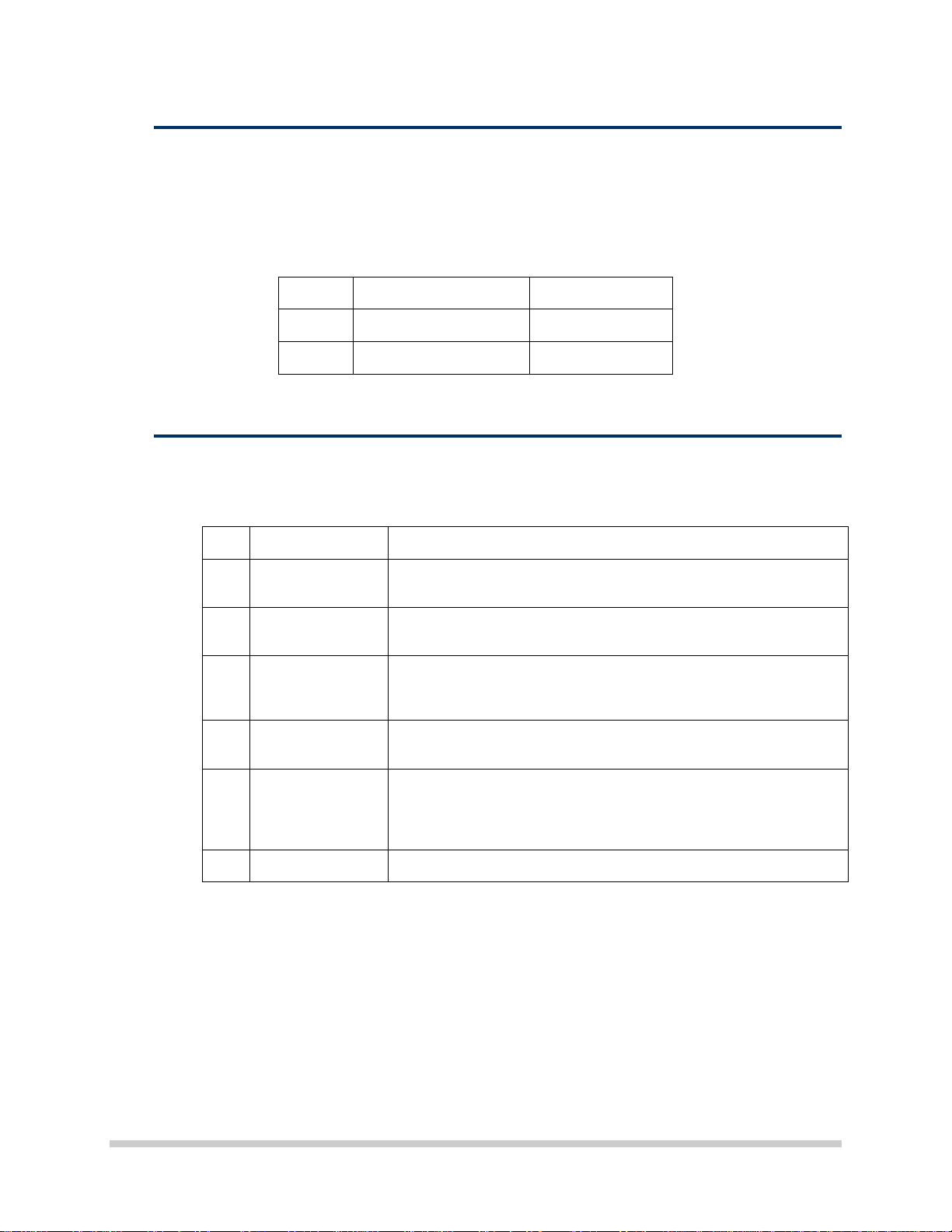
LED Expected function U3 Connection
D1 TX from USB CB0
D2 RX into USB CB1
Table 1: LED Connections
2.6 Primary Connector for Programming Interface
The connector J8 supports the programming interface for the remote hardware
(i.e. the JN5148 board that is to be programmed) and employs 3.3V signals.
Pin Name Use
1 DIO6 (input) Receive UART data, to connect to UART0 TXD output from remote
JN5148, i.e. DIO6.
2 DIO7 (output) Transmit UART data, to connect to UART0 RXD input of the JN5148,
i.e. DIO7.
3 MISO (output) Control line to connect to SPIMISO of the JN5148 – used in
conjunction with RESETN to put remote JN5148 into programming
mode. It is only possible to cause this pin to go low, due to diode D5.
4 3V30 3.3V supply output from programming interface. This is capable of
providing up to 40mA.
5 RESETN (output)
Control line to connect to RESETN of the JN5148 - used in
conjunction with MISO to put remote JN5148 into programming mode.
Also used to reset the JN5148 after a programming cycle. It is only
possible to cause this pin to go low, due to the diode D4.
6 GND Ground
Table 2: Pinout of J8 Connector
The connector takes the physical form of 6 plated vias at a 1.27-mm pitch, suitable
for direct soldering of a ribbon cable as shown in Figure 1. Pin 1 is identified by the
square pad in the Reference Design material. Ideally, the target application board
will have a 6-pin header specifically designed for this programming interface.

Jenni
c
USB Programming Dongle
Reference Manual
2.7 Extended Connector
The connector J1 is an alternative connector to J8. It has the same signals as J8
with the addition of DIO4 and DIO5, which can form the RTS and CTS UART
connections associated with DIO6 and DIO7. This connector employs 3.3V signals,
except the VCC signal is 5V (while it is 3.3V on the J8 connector). The connector
takes the physical form of 8 pads at a 2.54-mm pitch.
Pin Name Use
1 RESETN (output)
Control line to connect to RESETN of the JN5148 - used in
conjunction with MISO to put remote JN5148 into programming
mode. Also used to reset the JN5148 after a programming cycle. It
is only possible to cause this pin to go low, due to the diode D4.
2 GND Ground
3 DIO5 (input) CTS UART signal – to connect to remote UART0 RTS output,
i.e. DIO5 of JN5148.
4 VCCUSB 5V from the USB connector.
5 DIO7 (output) Transmit UART data, to connect to UART0 RXD input of the
JN5148, i.e. DIO7.
6 DIO6 (input) Receive UART data, to connect to UART0 TXD output from remote
JN5148, i.e. DIO6.
7 DIO4 (output) RTS UART signal – to connect to remote UART0 CTS input,
i.e. DIO4 of JN5148.
8 MISO (output) Control line to connect to SPIMISO of the JN5148 – used in
conjunction with RESETN to put remote JN5148 into programming
mode. It is only possible to cause this pin to go low, due to diode D5.
Table 3: Pinout of J8 Connector
JN-RM-2056 v1.0 © Jennic 2010 9

Jennic USB Programming Dongle
Reference Manual
10 © Jennic 2010 JN-RM-2056 v1.0
2.8 Configuring the FTDI Device
The FTDI device needs to be programmed in order for this Reference Design to
function as required. The FT_Prog tool provided on the FTDI web site
(www.ftdichip.com) should be used to program the device - the required
configuration is shown in Figure 3. It is necessary to first select the chip type,
FT232R, in the Chip_Details page.
Figure 3: Configuration Settings for FTDI device

Jenni
c
USB Programming Dongle
Reference Manual
3 Programming
In order to use the USB Programming Dongle to program the Flash memory device
on a remote JN5148-based application board, it is necessary to connect pins 1, 2, 3,
5 and 6 of the dongle board’s J8 connector to the application board. Pin 4 can also
be connected, if it is required to power the application board.
The JN51xx Flash programmer can then be used to program the Flash device – see
the JN51xx Flash Programmer User Guide (JN-UG-3007). This programming utility
will place the JN5148 into its programming mode by manipulating MISO and
RESETN on J8. It will then download the program to the Flash device and then reset
the JN5148, causing the application to be loaded and executed.
JN-RM-2056 v1.0 © Jennic 2010 11

Jennic USB Programming Dongle
Reference Manual
12 © Jennic 2010 JN-RM-2056 v1.0

Jenni
c
USB Programming Dongle
Reference Manual
Revision History
Version Date Description
1.0 24-Mar-2010 First release
JN-RM-2056 v1.0 © Jennic 2010 13

Jennic USB Programming Dongle
Reference Manual
14 © Jennic 2010 JN-RM-2056 v1.0
Important Notice
Jennic reserves the right to make corrections, modifications, enhancements, improvements and other changes to its
products and services at any time, and to discontinue any product or service without notice. Customers should
obtain the latest relevant information before placing orders, and should verify that such information is current and
complete. All products are sold subject to Jennic’s terms and conditions of sale, supplied at the time of order
acknowledgment. Information relating to device applications, and the like, is intended as suggestion only and may
be superseded by updates. It is the customer’s responsibility to ensure that their application meets their own
specifications. Jennic makes no representation and gives no warranty relating to advice, support or customer
product design.
Jennic assumes no responsibility or liability for the use of any of its products, conveys no license or title under any
patent, copyright or mask work rights to these products, and makes no representations or warranties that these
products are free from patent, copyright or mask work infringement, unless otherwise specified.
Jennic products are not intended for use in life support systems/appliances or any systems where product
malfunction can reasonably be expected to result in personal injury, death, severe property damage or
environmental damage. Jennic customers using or selling Jennic products for use in such applications do so at their
own risk and agree to fully indemnify Jennic for any damages resulting from such use.
All trademarks are the property of their respective owners.
Jennic Ltd
Furnival Street
Sheffield
S1 4QT
United Kingdom
Tel: +44 (0)114 281 2655
Fax: +44 (0)114 281 2951
For the contact details of your local Jennic office or distributor, refer to the Jennic web site:
Table of contents