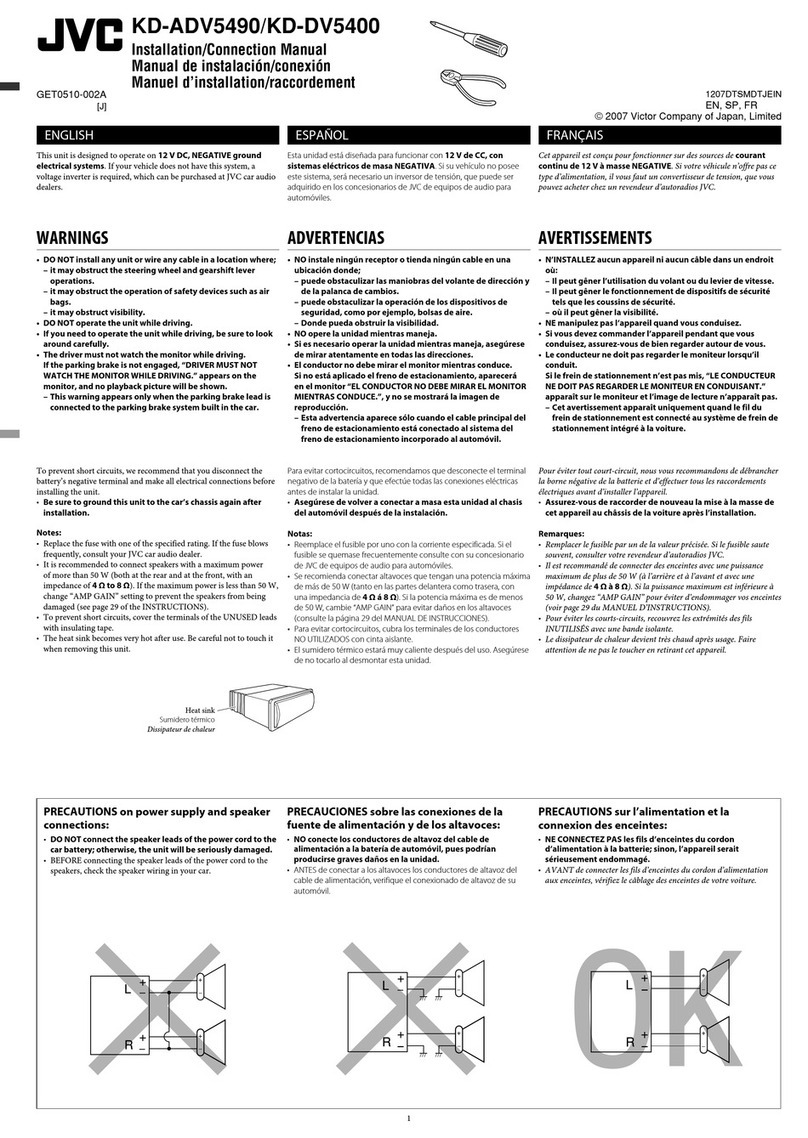
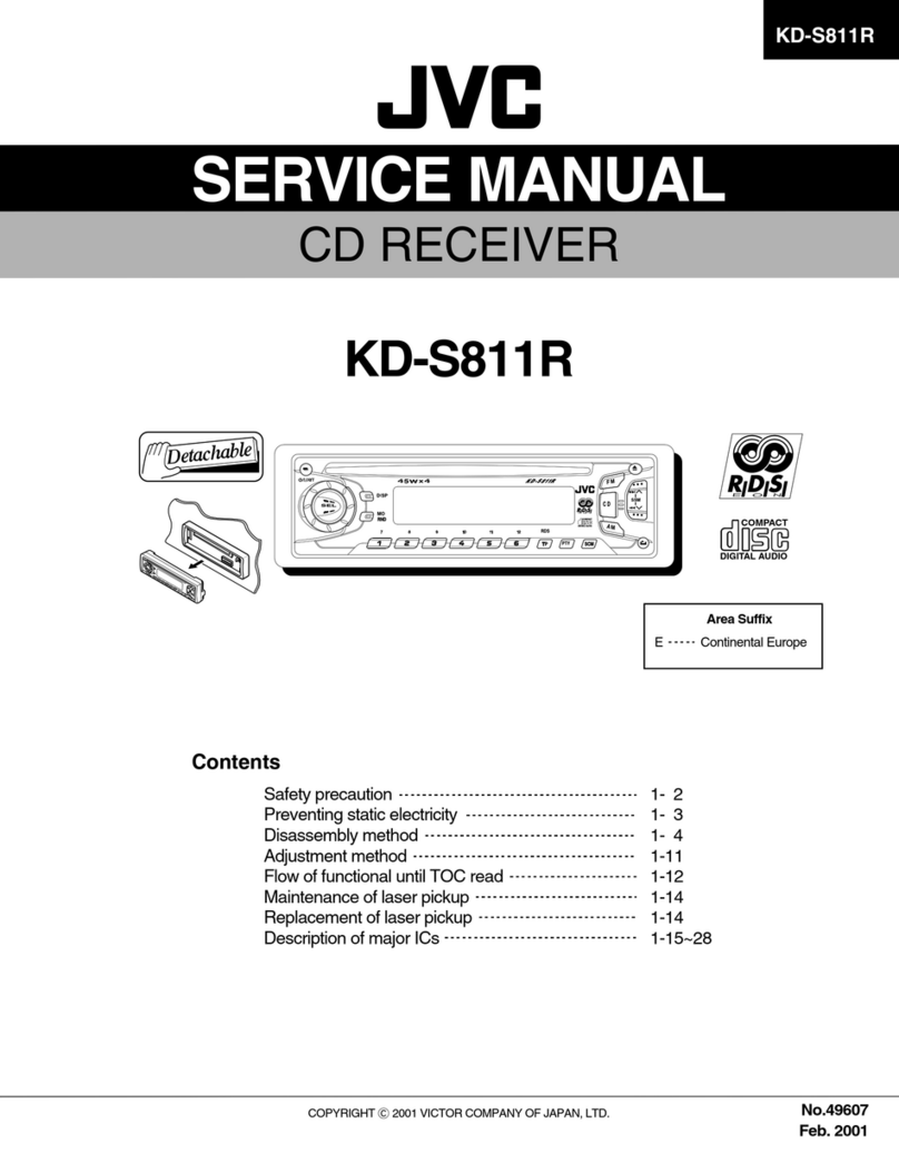
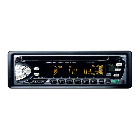
JVC KS-F350R User manual

SERVICE MANUAL
CASSETTE RECEIVER
No.49526
Dec. 1999
COPYRIGHT 1999 VICTOR COMPANY OF JAPAN, LTD.
This service manual is made from 100% redycled paper.
KS-F350R/KS-F353R
KS-FX450R/KS-FX453R
KS-F350R / KS-F353R
KS-FX450R / KS-FX453R
Area Suffix
E ---- Continental Europe
Contents
Safety precaution1-2
Instructions1-3~14
Location of main parts2-1
Disassembly method2-2
Adjustment method 2-7
Description of major ICs2-11
Block diagram2-19
Standard schematic diagrams2-20
Printed circuit boards2-23~24
Parts list3-1~15
ATT
FUNC
BAND
PROG
PRESET
DISC
DISC
Model
KS-F350R
KS-F353R
KS-FX450R
KS-FX453R
LCD
Color CD changer
controller
Ivory
Ivory
Amber
Amber
40Wx4
CD CHANGER CONTROL
AM
CD-
CH
FM
SOUND
PTY
SSM
PROG
TP
RDS
789101112
/I ATT
MO/FIND
DISP
SEL
KS-FX450R

!CAUTION Burrs formed during molding may be left over on some parts of the chassis. Therefore,
pay attention to such burrs in the case of preforming repair of this system.
Safety precaution

Location of main parts
Control unit
Main unit
Cassette mechanism
LED & key control board
Main board assembly
Display
Main board assembly
Motor control board Motor control board
Capstan motor unit
Capstan
motor unit Head amp board
Fly wheel
Head amp board
ISO connector
CD changer input jack
(Only for KS-FX450R/KS-FX453R)
Pin jack

Removal of main parts
Removing the front chassis
(See Fig.1)
1. Insert a screwdriver to the joints a on the side of the front
chassis and two joints b on the right side, then detach the
front chassis toward the front side.
Removing the heat sink (See Fig.2 )
1. Remove the three screws A attaching the heat sink on
the left side of the body, and remove the heat sink.
Removing the bottom cover (See Fig.3 )
1.
2.
3.
4.
Removing the front chassis.
Removing the heat sink.
Turn the body upside down.
Insert a screwdriver to the two joints c and two joints d on
both sides of the body and the joint d on the back of the
body, then detach the bottom cover from the body.
Removing the rear panel (See Fig.4 and 5 )
1.
2.
3.
4.
Remoe the front chassis.
Remove the heat sink.
Remove the bottom cover.
[KS-F350 / KS-F353]
Remove the three screws B attaching the rear panel and
one screws C attaching the pine jack on the back of the
body.
4. [KS-FX450 / KS-FX453]
Remove the Fore screws B' attaching the rear panel, one
screw C' attaching the pin jack and one screw D
attaching the C D changer input jack.
b
a
a
b
A
A
A
Heat sink
c
c
Front chassis
Fig.1
Fig. 2
Fig. 3
Fig. 4
[KS-F350 / KS-F353] Fig. 5
[KS-FX450 / KS-FX453]
Bottom cover
d
B
C
B
B
B'
CD changer input jack
C'
B'
B'
D
B'

Removing the main amplifier board assembly
(See Fig.4 and 5)
Removing the Cassette mehanism assembly
(See Fig.6)
1.
2.
3.
4.
5.
Remove the front chassis.
Remove the bottom cover.
Remove the rear pan.
Remove the two screws B attaching the main amplifier
board assembly on the top cover.
Disconnect connector CN901 and CN902 on the main
amplifier board assembly from the cassette mechanism
assembly.
1.
2.
3.
4.
Remove the front chassis.
Remove the bottom cover.
Remove the main amplifier board assembly.
Remove the tore screws F attaching the cassete
mechanism assembly from the top cover.
Removing the control switch board
(See Fig.7 and 8 )
1.
2.
3.
Remove the front panel unit from the main body.
Remove the four screws G attaching the rear cover on
the back of the front panel unit.
Remove the control switch board from the front panel
unit.
Fig.4
E
E
Cassete mechanism assembly
F
FF
Top cover
Fig. 6
GG
GG
Fig. 7 Fig. 8
Control switch board
CN901
Main amplifier board
F
CN902

(Cassette Mechanism Sections)
Head amplifier board
Direction
switch board
Motor assembly
Cassette hanger
Relay board
Center plate
Cassette holder
FF Lever
REW Lever
Chassis
Main belt
Sub-belt
Reel base assembly
Flywheel
assembly(B)
Flywheel
assembly(F)
8
7
77
Fig. 1 Fig. 2
Fig. 3
To see
Fig.5
Removing the Main Parts of Cassette Mechanism
1. Remove the cassette hanger and FF, REW, EJECT lever etc. , when you need to replace or adjusting head.
2. The main belt can be replaced directly.
3. To change the sub-belt, remove the three screws 7and loosen one screw 8.
Then raise the belt side of the reel base assembly slightly.
Removing the Cassette Hanger
(See Fig.1-5 )
1. From the rear of the unit, bend the
cassette hanger and chassis the five claws
a, boutwards.
2. While pressing the EJECT lever, remove the
cassette hanger.
3. Remove the return ink rod from the center plate
of the cassette hanger.
Cassette hanger
Center plate
Return link
EJECT lever
Chassis
Claw
Claw

Note : The reel disk and capstan can now
be replaced.
1-1 Remove the C washer at the top of the reel disk to
remove the reel disk.
caution : Replace with a new C washer after repairing.
1-2 To replace the capstan, remove the E washer in the
pinch-roller section.
Remove the main belt of the flywheel beforehand.
Assembling the Cassette Hanger ( See Fig. 1-5)
1. Assemble the return link.
2. Install the cassette hanger on the chassis.
Note : While pressing the EJECT lever, assemble
in the order shown below.
C Washer
Reel disk
Capstan
E Washer
Cassette hanger
Return link EJECT lever
EJECT L.Spring
EJECT C.Spring
EJECT cam
The convex section should be between
the cassette hanger and EJECT cam .
Fig. 4
Fig. 5
Fig. 6
Removing the FF/REW lever assembly
( See Fig. 6)
1. From the rear of unit, remove the FF/REW lever
assembly retaining the one screw1.
2. From the upper part of the FF/REW lever assembly,
remove the FF/REW lever assembly
retaining the one screw 2.
3. From the front of unit, remove the FF/REW lever
assembly upwards and pull it slightly to the front.
Assembling the FF/REW lever Assembly
1. Assemble the FF/REW lever assembly to the
chassis of rear section c.
2. Assemble the pinch-roller shaft d, change
lever(B) eand return link fto chassis.
FF/REW lever assembly
2

Fig. 7
Fig. 10
Fig. 9
Fig. 8
Removing the Pinch-Roller assembly ( See Fig. 7)
1. Remove the two E Washers 3retaining the pinch-roller shaft.
2. Remove the P.Arm spring (F) from the chassis.
3. Remove the P.Arm spring (R) from the chassis.
4. Pull out the pinch-roller(F,R) assemblies from the left
and right sides.
Note : The P.arm spring (F) and P.arm spring (R) are different.
Note : The Pinch-roller (F) and Pinch-roller(R)assemblies
are different.
Removing the Playback Head ( See Fig. 7 )
1. Remove the one fixed screw 4retaining the playback head.
2. Remove the C Washer 5to pull the FF roller out .
3. Remove the S. support plate to remove the A.arm springs
(A,B) and playback head.
Note : The A. arm spring (A) and A. arm spring (B) are different.
Removing the Motor Assembly ( See Fig. 8 )
1. Remove the main belt and sub-belt from the back side unit.
2. Remove the two screws 6retaining the motor assembly.
Changing the Sub-Belt ( See Fig. 8 )
1. Remove the main belt from the back side unit..
2. Remove the sub-belt from the motor pulley.
3. Remove the four screws 7, 8retaining
the reel base assembly.
4. Lift up the reel base assembly slightly to
change the belt.
Removing the Reel Base Assembly ( See Fig. 8-10)
1. Remove the selector link (B) from the front unit by turning
the selector link (B) near the pinch-roller as shown
in the figure 9.
3. Remove the four screws 7, 8retaining the reel base
assembly.
4. Remove the reel base assembly carefully.
Note : Service for the reel base assembly is not available.
P. arm spring(F)
P. arm spring(R)
33
E Washer E Washer
Pinch-roller
shaft Pinch-roller shaft
Pinch-roller (R)
assembly
Pinch-roller (R)
assembly
Pinch-roller (F)
assembly
A.arm
spring(A)
A.arm
spring(B)
Remove the P. arm spring (F)
from the chassis.
S. support plate
Main belt Sub belt
Reel base assembly
Motor assembly
Motor pulley
Selector link (B) Turn the selector link (B)
disengage this one.
Back side view of the reel base assembly
Adjustment method
Test Instruments reqired for adjustment
1. Digital osclloscope(100MHz)
2. Frequency Counter meter
3. Electric voltmeter
4. Wow & flutter meter
5. Test Tapes
VT724 ....................... for DOLBY level measurement
VT739 ............ For playback frequency measurement
VT712 ....For wow flutter & tape speed measurement
VT703 ..................... For head azimuth measurement
6. Torque gauge .................... Cassette type for CTG-N
(mechanism adjustment)
Measuring conditions(Amplifier section)
Power supply voltage .............. DC14.4V (10.5 - 16V)
Load impedance ........... 4 (2Speakers connection)
Line out............................................................ 20k
Standard volume position
Balance and Bass,Treble volume .Fader
:Center(Indication"0")
Loudness,Dolby NR,Sound,Cruise:Off
Volume position is about 2V at speaker output with
following conditions.Playback the test tape VT721.
AM mode 999kHz/62dB,INT/400Hz,30%
modulation signal on recieving.
FM mono mode 97.9MHz/66dB,INT/400Hz,22.5kHz
deviation pilot off mono
FM stereo mode 1kHz,67.5kHz dev. pilot7.5kHz dev.
Output level 0dB(1 V,50 /open terminal)
Frequency Band
FM 87.5-108MHz 50KHz step
Band MW 522-1620KHz 9KHz step
LW 144-279KHz

Arrangement of adjusting & test points
Head section view
Cassette mechanism
(Surface)
Tape speed adjust
Motor assembly
Playback head
Azimuth screw
Head azimuth screw Fixed screw
Height adjusting screw c
Height adjusting screw b
Height adjusting screw a
Playback head

Extension cord
: EXTKSRT002-6P
EXTKSRT002-6P
Front panel assembly
Main board
Cassette mechanism
Information for using a car audio service jig
1. For 1995 and 1996 , we're advancing efforts to make our extension cords common for all car audio products.
Please use this type of extension cord as follows.
2. As a U-shape type top cover is employed, this type of extension cord is needed to check operation of the
mechanism assembly after disassembly.
3. Extension cord : EXTKSRT002-6P ( 6 pin extension cord ) For connection between mechanism assembly
and main board assembly.
Check for mechanism driving section such as motor ,etc..
Disassembly method
1. Remove the bottom cover.
2. Remove the front panel assembly.
3. Remove the top cover .
4. Install the front panel.
5. Confirm that current is being carried by connecting
an extension cord jig.
Note
Available to connect to the CN701 connector when in-
stalling the front panel.

Mechanism adjustment section
Item Adjusting & Confirmation Methods Adjust Std. Value
"Head Height Adjustment"
Note
Adjust the azimuth directly. When you adjust the height us-
ing a mirror tape, remove the cassette housing from the
mechanism chassis.
After installing the cassette housing, perform the azimuth
adjustment.
1.load the mirror tape ( SCC-1659 ). Adjust with height
adjustmentscrew (a) and azimuth adjustment screw (b) so
that line "A" of the mirror tape runs in the center between
Lch and Rch in the reverse play mode.
2.After switching from REV to FWD then to REV, check that
the head position set in procedure "1" is not changed.
*If the position has shifted, adjust again and check.
3.Adjust the azimuth screw (b) so that line "B" of the mirror
tape runs in the center between Lch and Rch in the forward
play mode.
"Head Azimuth Adjustment"
1.Load the test tape ( VT724: 1kHz ) and play it back in the
reverse play mode. set the Rch output level to maximum.
2.Load the test tape ( VT703: 10kHz ) and play it back in the
forward play mode. Adjust the Rch and Lch output levels
tomaximum, with azimuth adjustment screw (b).
In this case, the phase difference should be within 45 .
3.Engage the reverse mode and adjust the output level to
maximum, with azimuth adjustment screw (c).
*The phase difference should be 45_Kor more.
4.When switching between forward and reverse modes, the
difference between channels should be within 3dB.
*Between FWD Lch and Rch, REV Lch and Rch.
5.When the test tape ( VT721 : 315Hz ) is played back, the
level difference between channels should be within 1.5dB.
1.Check to see if the reading of the frequency counter & Wow
flutter meter is within 2940-3090 Hz( FWD/REV ), and less
than 0.35% ( JIS RMS ).
2.In case of out of specification, adjust the motor with a built-
in volume resistor.
1.Play the test tape ( VT724 : 1kHz ) back and set the volume
position at 2V.
2.Play the test tape ( VT739 )back and confirm 0 +3dB at1kHz/
-
8kHz and -4+2dB at 1kHz/125Hz.
3.When 8kHz is out of specification, it will be necessary to
read adjust the azimuth.
Head shield
Head shield
The head is at low position
during FWD.
The head is at height position
during REV.
A Line
B Line
Phase
screw (c) screw (a)
screw (b)
Head azimuth
screw Fixed screw
045
Built-in
volume resistor Tape Speed
2940-3090Hz
Wow&Flutter
Less than
0.35%
(JIS RMS)
Speaker out
1kHz/8kHz
: 0dB_}3dB,
125Hz/1kHz
: -4dB+2dB,
1.Head azimuth
2.Tape Speed and
Wow & Flutter
3.Playback
Frequency
response

AN80T05LF (IC961) : Regulator
1. Block diagram
-
+
-
+-
+
-
+-
+
ILL
10V MODE2 MODE1 STB VDD VCC
5.6V AMP ANT COM
8.7V 8.7V 8.7V
AM FM GND
Reference Voltage
ASO & Peak
Current Protection
Thermal
Protection
Pre
Drive Pre
Drive Pre
Drive
Pre
Drive Pre
Drive
AMT
Out
AMT
Out
12345 6 78910 11 12
2.Pin Function
Illumination output
MODE2 SW
MODE1 SW
STAND BY
VDD output
AMP output
VCC
ANT output
COM output
AM output
FM output
GND
1
2
3
4
5
6
7
8
9
10
11
12
10V power supply with a maximum output current of 300mA for a illumination.
AM and ANT output are turned ON when this pin is 5V.
AM and FM output are switched when this pin is 5V.
Only VDD output during the 0V standby state; ILL,COM and AMPoutputs
are turuned ON when this pin is 5V.
5.6V Power supply with amaximum output current of 100mA for a micro-
controiler. Output is always available if BACKUP power supply is connected.
Power supply to activate a remote amplfier; a voltage of about 1V(typ) lower
than VCC voltage is provided with a maximum output current of 500mA.
Connected to car BACKUP and ACC Power supplioes.
Power supply to drive an antenna voltage of about 1V(Tpy) lower than the VCC
voltage is provided with amaximum output current of 500mA.
8.7V power supply with a maximum output current of 150mA; this can be used
as a system common power supply.
8.7V power supply with a maximum output current of 150mV for AM receiver.
8.7V power supply with a maximum output current of 150mV for FM receiver.
Connected to the IC substrate.
Function
Pin name
Pin
No.
Description of major ICs

HA13158A (IC941) : Power amp
1. Pin layout
2. Block diagram
IN1
IN2
IN3
IN4
STBY
2
1
11
13
23
10
TAB
PROTECTOR (ASO
SURGE, TSD)
INPUTBUFFER1
INPUTBUFFER2
INPUTBUFFER3
INPUTBUFFER4
AMP1
AMP2
AMP3
AMP4
MUTE
PVCC1PVCC2
INVCC
+
-
+
-
+
-
+
-
12 22
14 18 6
3
4
5
7
8
9
15
16
17
19
20
21
1 ~ 23

Vcc Vcc
Input
See Function Table
1A
2A
3A
4A
1C
2C
3C
4C
1Y
2Y
2Y
3Y
4Y
Output
Output
Output
Output
Sample as Load Circuit 1
1k
1k
S1
CL
Inputs Outputs
C
L
H
H
A
X
L
H
Y
Z
H
L
1
2
3
4
5
6
7
14
13
12
11
10
9
8
HD74HC126FP-X (IC751) : Buffer
1. Pin layout
3. Block diagram
2. Function

AMP1
AMP2
UPC1228HA
1
2
3
4
5
6
7
8
IN1
NFB1
OUT1
VCC
GND
OUT2
NFB2
IN2
UPC1228HA(IC901):Head amp

QUAL
RDDA
RDCL
T57
VSDDTESTMODEVSSA
OSCI OSCO VDDD
SCOUT
MUX
CIN
VDDA
Vref
4
8
7
5
3
6
Vp1
9 10 11
15
16
2
1
13 14 12
ANTI-
ALIASING
FILTER
RECONSTRUCTION
FILTER
OSCCILLATOR
AND
DIVIDER
DIFFERRENTIAL
DECODER
QUALITY BIT
GENERATOR
BIPHASE
SYMBOL
DECODER
TEST LOGIC AND OUTPUT
SELECTOR SWITCH
57kHz
BANDPASS
(8th ORDER)
CLOCKED
COMPARATOR
CLOCK
REGENERATION
AND SYNC
REFERENCE
VOLTAGE
COSTAS LOOP
VARIABLE AND
FIXED DIVIDER
SAA6579T-X (IC761) : RDS Detector
1. Pin layout 2. Pin function
3. Block diagram
1
2
3
4
5
6
7
8
16
15
14
13
12
11
10
9
1
2
3
4
5
6
7
8
9
10
11
12
13
14
15
16
Quality indication output
RDS data output
Reference voltage output (0.5VDDA)
Multiplex signal input
+5V supply voltage for anarog part
Ground for analog part (0V)
Subcarrier input to comparator
Subcarrier output of reconstruction filter
Oscillator mode / test sontrol input
Test enable input
Ground for digital part (0V)
+5V supply voltage for digital part
Oscillator input
Oscillator output
57kHz clock signal output
RDS clock output
QUAL
RDDA
Vref
MUX
VDDA
VSSA
CIN
SCOUT
MODE
TEST
VSSD
VDDD
OSCI
OSCO
T57
RDCL
Pin
No. Symbol Function

1
2
3
4
5
6
7
8
9
10
11
12
13
14
15
16
32
31
30
29
28
27
26
25
24
23
22
21
20
19
18
17
SDA
GND
OUTLR
OUTLF
TL
B2L
B1L
IVL
ILL
QSL
IDL
MUTE
ICL
IMD
IBL
IAL
SCL
VCC
OUTRR
OUTRF
TR
B2R
B1R
IVR
ILR
QSR
IDR
Vref
ICR
CAP
IBR
IAR
CD-CH
TAPE
TUNER
POWER
SUPPLY
SOURCE
SELECTOR
VOLUME 1
+20 to -31 dB
LOUDNESS
LEFT
BASS
LEFT
+15 dB
TREBLE
LEFT
+12 dB
BASS
RIGHT
+15 dB
TREBLE
RIGHT
+12 dB
MUTE
FUNCTION
ZERO CROSS
DETECTOR
VOLUME 2
0 to 55 dB
BALANCE
FENDER REAR
VOLUME 2
0 to 55 dB
BALANCE
FENDER FRONT
HC BUS
REC
VOLUME 2
0 to -55dB
BALANCE
FENDER FRONT
VOLUME 2
0 to -55dB
BALANCE
FENDER REAR
VOLUME 1
+20 to -31 dB
LOUDNESS
RIGHT
LOGIC
21
31
2
19
16
15
13
11
22
20
18
17
14
23 25 24 26 27 28
30
29
1
32
3
4
10 8 9 7 6 512
1.Pin Layout
3.Pin Functions
2.Block Diagram
1
2
3
4
5
6
7
8
9
10
11
12
13
14
15
16
Pin
No. Pin
No.
17
18
19
20
21
22
23
24
25
26
27
28
29
30
31
32
SDA
GND
OUTLR
OUTLF
TL
B2L
B1L
IVL
ILL
QSL
IDL
MUTE
ICL
IMO
IBL
IAL
Serial data input/output.
Ground.
output left rear.
output left front.
Treble control capacitor left channel or
input from an external equalizer.
Bass control capacitor left channel or
output to an external equalizer.
Bass control capacitor left channel.
Input volume 1. left control part.
Input loudness. left control part.
Output source selector. left channel.
Not used
Not used
Input C left source.
Not used
Input B left source.
Input A left source.
I/O
-
O
O
I
-
-
I
I
O
-
-
I
-
I
I
Symbol I/O Symbol I/O
Input A right source.
Input B right source.
Electronic filtering for supply.
Input C right source.
Reference voltage (0.5Vcc)
Not used
Output source selector right channel.
Input loudness right channel.
Input volume 1. right control part.
Bass control capacitor right channel
Bass control capacitor right channel or
output to an external equalizer.
Treble control capacitor right channel or
input from an external equalizer.
Output right front.
Output right rear.
Supply voltage.
Serial clock input.
I
I
-
I
-
-
O
I
I
-
O
I
O
O
-
I
IAR
IBR
CAP
ICR
Vref
IDR
QSR
ILR
IVR
B1R
B2R
TR
OUTRF
OUTRR
Vcc
SCL
Functions Functions
TEA6320T-X (IC911) : E.VOLUME

1
2
3
4
5
6
7
8
9
10
11
12
13
14
15
16~20
21
22
23
24
25
26
27
28
29
30
31
32
33
34
35
36
37
38
39
40
41
42
43
44
45
46
47
48
49
50
51
52
53
54
55
56
57
58
59
60
61
62~66
67
68
69
70
71
72
73
74
75
76
77
78
79
80
KEY0
KEY1
KEY2
LEVEL
SM
SQ
LCDCE
LCDDA
LCDSCK
BUSI/O
UNLOCK
BUSSI
BUSSO
BUSSCK
MUTE
NC
GNDPORT
VDDPORT
AM
AFCK
MONO
FM
SEEK/STOP
NC
IFC
VDDPLL
FMOSC
AMOSC
GNDPLL
AMEO
FMEO
IC
SD/ST
STAGE
NC
F/R
NC
NC
TELMUTE
TAPEIN
I2CSCK
I2CDAO
I2CDAI
NC
NC
T-MUTE
NC
NC
NC
NC
TAPE
TUNER
CD
NC
NC
MUTE
POWER
NC
ON
STOP
RDSCK
RDSDA
REMOCON
DETACH
JBUS INT
REGCPU
GND
X2
X1
REGOSC
VDD
/RESET
I
I
I
O
I
I
O
O
O
O
O
I
O
O
O
O
-
-
O
O
O
O
O
I
I
-
I
I
-
O
O
-
I
I
I
I
O
O
O
I
I/O
O
I
O
O
O
O
O
O
O
O
O
O
O
O
O
O
I
I
I
I
O
I
I
-
-
-
-
-
-
I
Key input 0
Key input 1
Key input 2
Non connect
Signal meter input
Signal quality input
Chip enable output to LCD driver
Data output to LCD driver
Clock output to LCD driver
I/O switch output for J-BUS
Unlock output for PLL L:unlock H:lock
Data input for J-BUS
Data output for J-BUS
Clock output for J-BUS
Mute output L:mute
Non connect
GND for port
VDD for port
Output for AM power supply H:AM Mode
AF check output L:AF check
Monaural ON/OFF output H:Monaural ON
Output for FM power supply H:FM Mode
Auto seek/Stop output H:Aut seek L:Stop
Non connect
FM/AM limited generator frequency input
VDD for PLL
FM/AM limited generator frequency input
Non connect
GND for PLL
Error out output for AM
Error out output for FM
Direct connecting to ground
Seek/Stop port H:SD input
Seek/Stop port L:Stereo input
Initial establihing port,L:None disc
Momentary key is two mode.
Non connect
Forward, reverse switching input.
H:Forward L:Reverse
Non connection
Non connection
Non connection
Cassette in detect input H:OUT L:IN
Clock in/output for electrical volume IC control
Data output for electrical volume IC control
Data input for electrical volume IC controt
Non connection
Non connection
Non connection
Non connection
Non connection
Non connection
Non connection
"H" at TAPE mode is output
"H" at TUNER mode is output
"H" at CD mode is output
Non connection
Non connection
Non connection
Power output, H:power ON
Non connect
On input, H:Action mode L:Power save mode
Input for stop mode
Clock input for RDS
Data input for RDS
Non connection
Detach input,Action mode L by more than
200ms, H:power save mode
Cut-in input for J-BUS.
Connects the graund with capacitor 0.1 F.
Ground
Connect the crystal oscillator for system clock.
Connects the graund with capacitor 0.1 F.
Power supply
Connect the VDD with resistor.
Pin
No. Symbol I/O Function Pin
No. Symbol I/O Function
UPD178016AGC513(IC701):System Controller Micon
20 ~ 1
41 ~ 60
21
40
80
61
~
~
1.Terminal Layout
2.Description

1
2
3
4
5
6
7
8
9
10
11
12
13
14
15
16
S1
S2
S3
S4
S5
S6
S7
S8
S9
S10
S11
S12
S13
S14
S15
S16 17 18 19 20 21 22 23 24 25 26 27 28 29 30 31 32
48
47
46
45
44
43
42
41
40
39
38
37
36
35
34
33
S48
S47
S46
S45
S44
S43
S42
S41
S40
S39
S38
S37
S36
S35
S34
S33
64 63 62 61 60 59 58 57 56 55 54 53 52 51 50 49
S17
S18
S19
S20
S21
S22
S23
S24
S25
S26
S27
S28
S29
S30
S31
S32
DI
CL
CE
OSC
Vss
VDD2
VDD1
INH
VDD
COM3
COM2
COM1
S52
S51
S50
S49
LC75823W (IC651) : LCD Driver
1. Pin Layout & Symbol
2. Pin Function
Pin No.
1 to 52
53 to 55
56
57
58
59
60
61
62
63
64
I/O
O
O
--
I
I
I
--
I/O
I
Segment output pins used to display data transferred
by serial data input.
Common driver output pins. The frame frequency is given
by : t0=(fosc/384)Hz.
Power supply connection. Provide a voltage of between
4.5 and 6.0V.
Display turning off input pin.
INT="L" (Vss) ----- off (S1 to S52, COM1 to COM3="L"
INT="H" (VDD)----- on
Serial data can be transferred in display off mode.
Used for applying the LCD drive 2/3 bias voltage
externally.
Must be connected to VDD2 when a 1/2 bias drive scheme
is used.
Used for applying the LCD drive 1/3 bias voltage
externally.
Must be connected to VDD1 when a 1/2 bias drive scheme
is used.
Power supply connection. Connect to GND.
Oscillator connection.
An oscillator circuit is formed by connecting an external
resistor and capacitor at this pin.
Serial data CE : Chip enable
interface connection
to the controller. CL : Sync clock
DI : Transfer data
Symbol
S1 to S52
COM1 to COM3
VDD
INH
VDDD1
VDD2
Vss
OSC
CE
CL
DI
Function
Other manuals for KS-F350R
2
This manual suits for next models
3
Table of contents
Other JVC Car Receiver manuals

JVC
JVC KD-T925BTS User manual

JVC
JVC KD-R741BT User manual

JVC
JVC KD-AR7500 - Radio / CD User manual

JVC
JVC GET0063-001A User manual

JVC
JVC CD/Cassette Receiver KW-XC939 Guide

JVC
JVC KD-DV5307 User manual

JVC
JVC KW-XC105 Guide

JVC
JVC KD-AR760 - Arsenal CD Receiver Guide

JVC
JVC KD-S743R User manual

JVC
JVC KD-G847 User manual