AV29A10EUS
No.51818
AV29A10EUS
Sept. 2001 No.51818
2-32 VP0109
DP6051
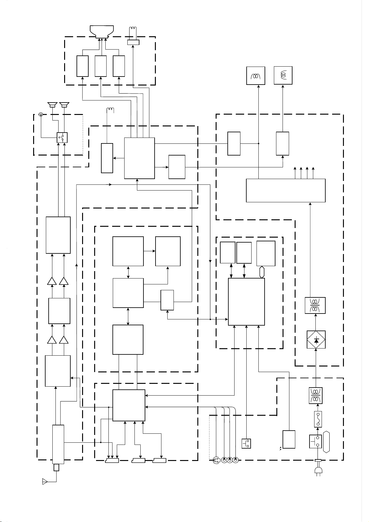
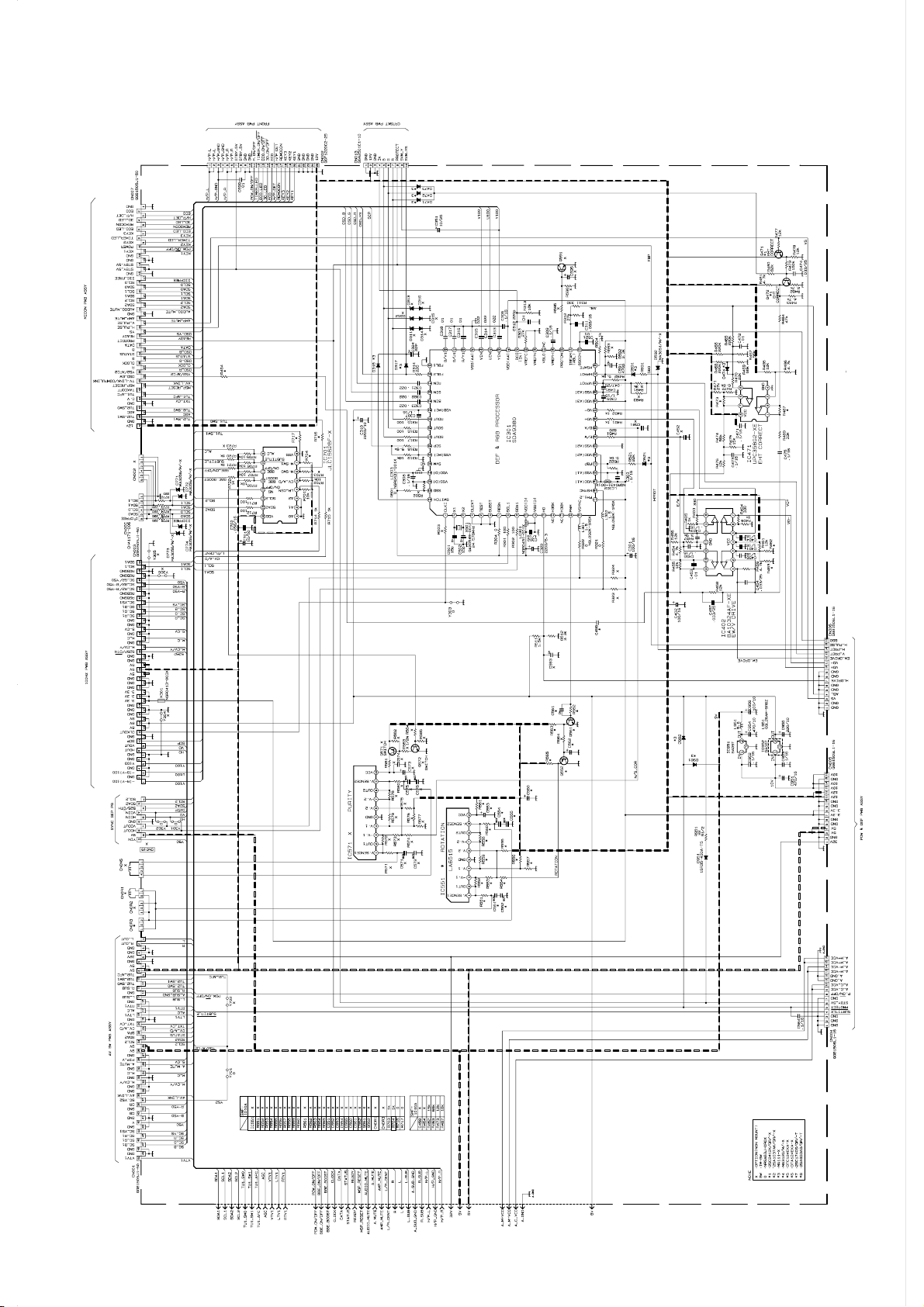
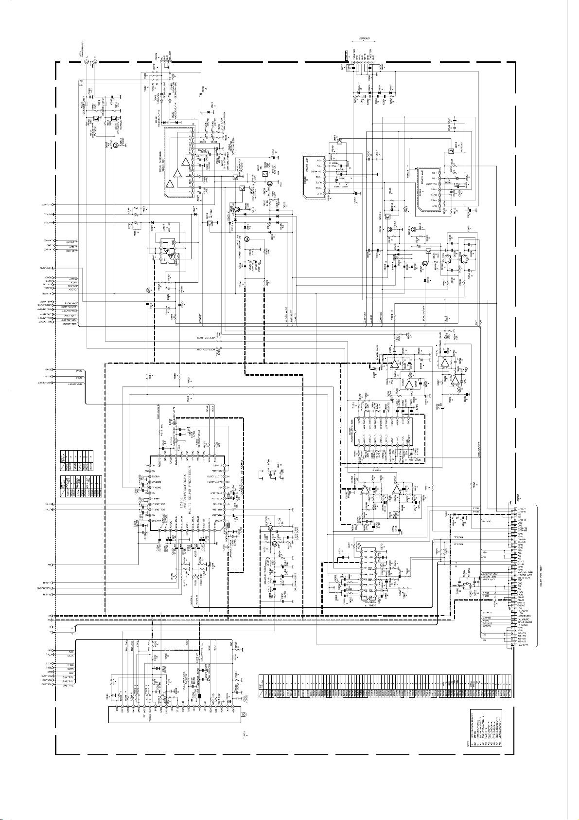
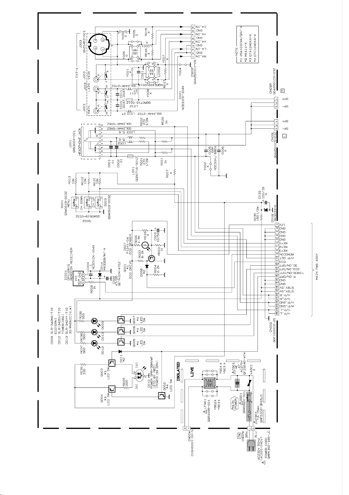
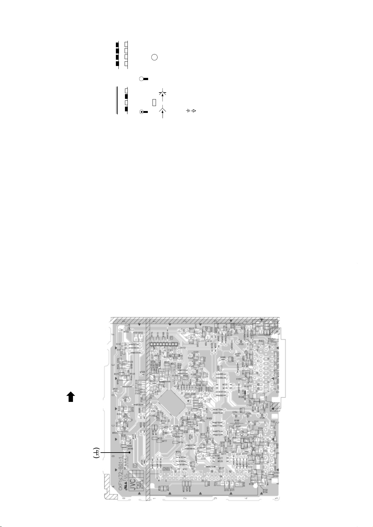
AV SW PWB PATTERN STANDARD CIRCUIT DIAGRAM
n
NOTE ON USING CIRCUIT DIAGRAMS
1.SAFETY
The components dent f ed by the
symbol and shad ng are
cr t cal for safety. For cont nued safety replace safety cr t cal
components only w th manufactures recommended parts.
2.SPECIFIED VOLTAGE AND WAVEFORM VALUES
The voltage and wave orm values have been measured under the
ollowing conditions.
(1)Input signal : Color bar signal
(2)Setting positions o
each knob/button and
variable resistor
(3)Internal resistance o tester :DC 20k¶/V
(4)Oscilloscope sweeping time :H Ë 20µS/div
:V Ë 5mS/div
:Others Ë Sweeping time is
speci ied
(5)Voltage values :All DC voltage values
Since the voltage values o signal circuit vary to some extent
according to adjustments, use them as re erence values.
3.INDICATION OF PARTS SYMBOL [EXAMPLE]
In the PW board :R1209¨R209
4.INDICATIONS ON THE CIRCUIT DIAGRAM
(1)Res stors
Resistance value
No unit :[¶]
K :[K¶]
M :[M¶]
Rated allowable power
No indication :1/16 [W]
Others :As speci ied
Type
No indication :Carbon resistor
OMR :Oxide metal ilm resistor
MFR :Metal ilm resistor
MPR :Metal plate resistor
UNFR :Unin lammable resistor
FR :Fusible resistor
*Composition resistor 1/2 [W] is speci ied as 1/2S or Comp.
(2)Capac tors
Capacitance value
1 or higher :[pF]
less than 1 :[µF]
Withstand voltage
No indication :DC50[V]
Others :DC withstand voltage [V]
AC indicated :AC withstand voltage [V]
*Electrolytic Capacitors
47/50[Example]:Capacitance value [µF]/withstand voltage[V]
Type
No indication :Ceramic capacitor
MY :Mylar capacitor
MM :Metalized mylar capacitor
PP :Polypropylene capacitor
MPP :Metalized polypropylene capacitor
MF :Metalized ilm capacitor
TF :Thin ilm capacitor
BP :Bipolar electrolytic capacitor
TAN :Tantalum capacitor
(3)Co ls
No unit :[µH]
Others :As speci ied
(4)Power Supply
:B1 :B2(12V)
:9V :5V
*Respective voltage values are indicated
(5)Test po nt
:Test point :Only test point display
(6)Connect ng method
:Connector :Wrapping or soldering
:Receptacle
(7)Ground symbol
:LIVE side ground
:ISOLATED(NEUTRAL) side ground
:EARTH ground
:DIGITAL ground
5.NOTE FOR REPAIRING SERVICE
This models power circuit is partly di erent in the GND. The
di erence o the GND is shown by the LIVE : () side GND and the
ISOLATED(NEUTRAL) : () side GND. Thereore, care must be
taken or the ollowing points.
(1)Do not touch the LIVE side GND or the LIVE side GND and the
ISOLATED(NEUTRAL) side GND simultaneously. I the above
caution is not respected, an electric shock may be caused.
There ore, make sure that the power cord is surely removed rom
the receptacle when, or example, the chassis is pulled out.
(2)Do not short between the LIVE side GND and
ISOLATED(NEUTRAL) side GND or never measure with a
measuring apparatus ( oscilloscope, etc.) the LIVE side GND and
ISOLATED(NEUTRAL) side GND at the same time. I the above
precaution is not respected , a use or any parts will be broken.
S nce the c rcu t d agram s a standard one, the c rcu t and
c rcu t constants may be subject to change for mprovement
w thout any not ce.
NOTE
Due mprovement n performance, some part numbers show
n the c rcu t d agram may not agree w th those nd cated n
the part l st.
When order ng parts, please use the numbers that appear n
the Parts L st.
:Original setting position
when shipped
TOP