TAC
70
KENWOOD
SERVICE
MANUAL
©
1989-11
PRINTED
IN
JAPAN
B51-8038-00
(O)
588
Knob
Knob
(POWER
SW)
Metallic
cabinet
Knob
Front
glass
Panel
ass'y
(DRESSING
PANEL)
(K29-4540-14)
(K29-4519-04)
{A01-1087-02)
(K29-4540-14)
(B10-1129-14)
|
(A20-7061-04)
Knob
(K29-4540-14)
x
4
S68
AAG
OTE
EPHONE
Microphone
Phone
jack
Label
Knob
(MAIN
DIAL)
Foot
Knob
(T91-0388-05)
(E11-0440-05)
(B42-3379-04)
(K29-4538-03)
(J02-0323-05)
x
4
(K29-4539-04)
x
2
CONTENTS
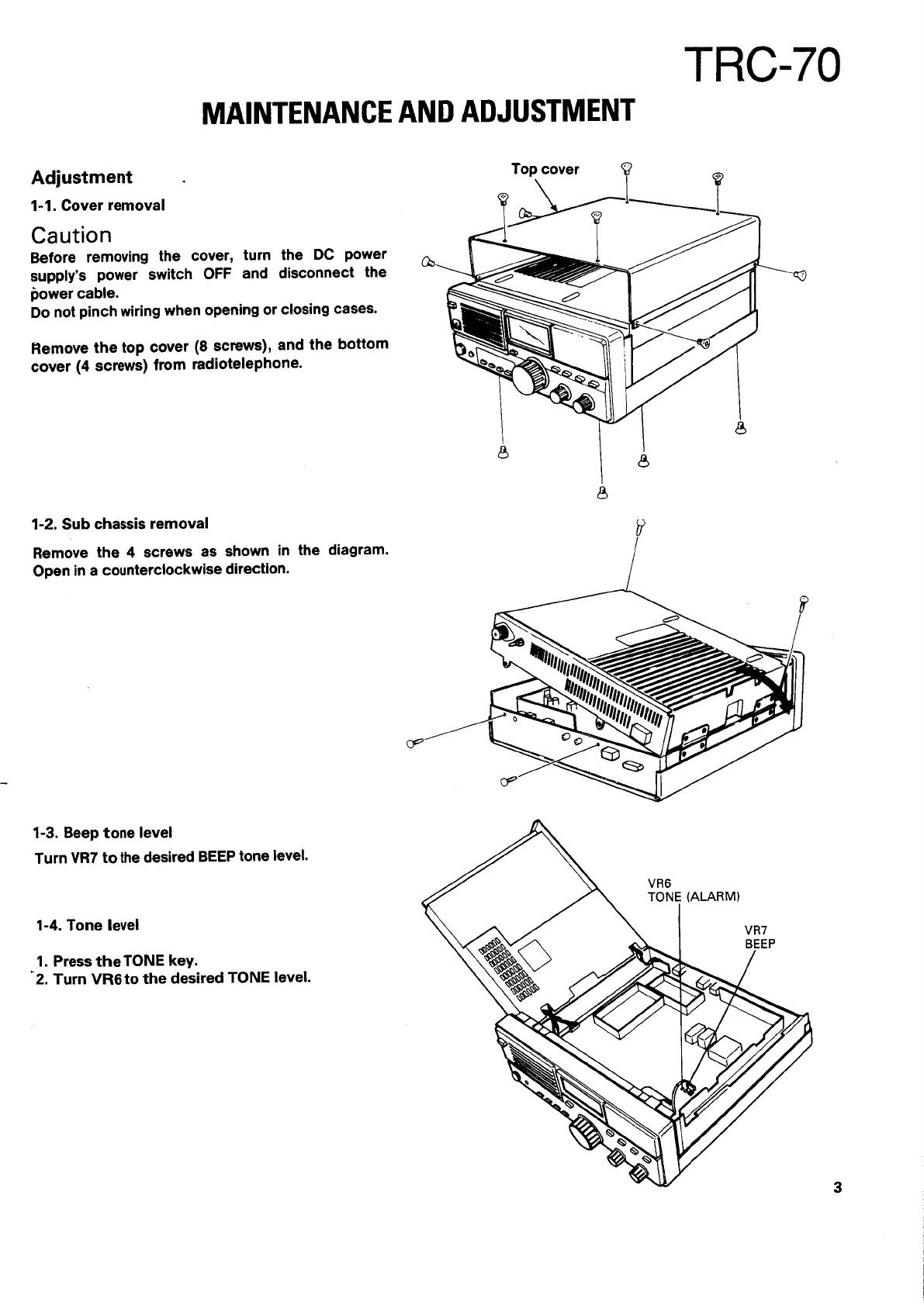
MAINTENANCE
AND
ADJUSTMENT
............cccccee
2
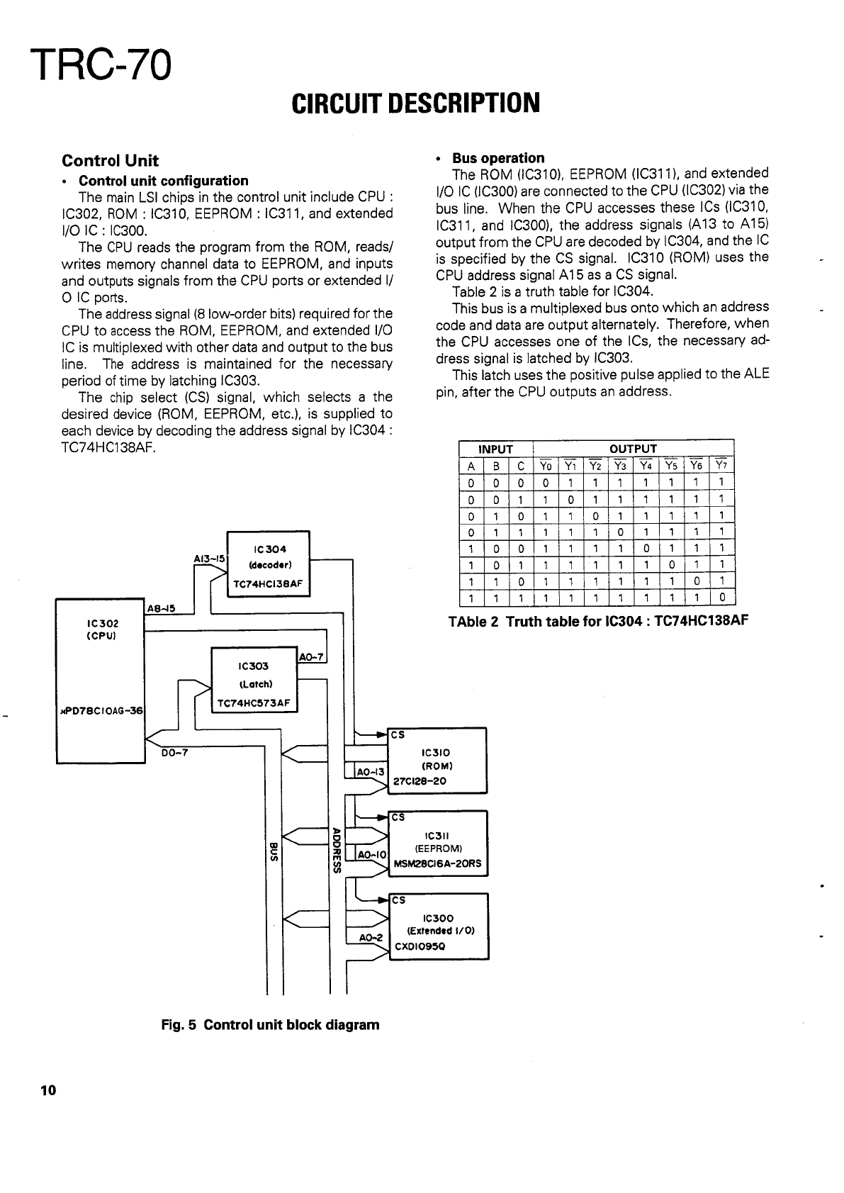
CONTROL
UNIT
(X53-3280-21)
.......ccccceensereenees
85
INSTALLATION
INSTRUCTIONS.
...........cscsceseners
5
TX-RX
UNIT
(X57-3470-21)
oc
eccscceccceenssenseresens
93
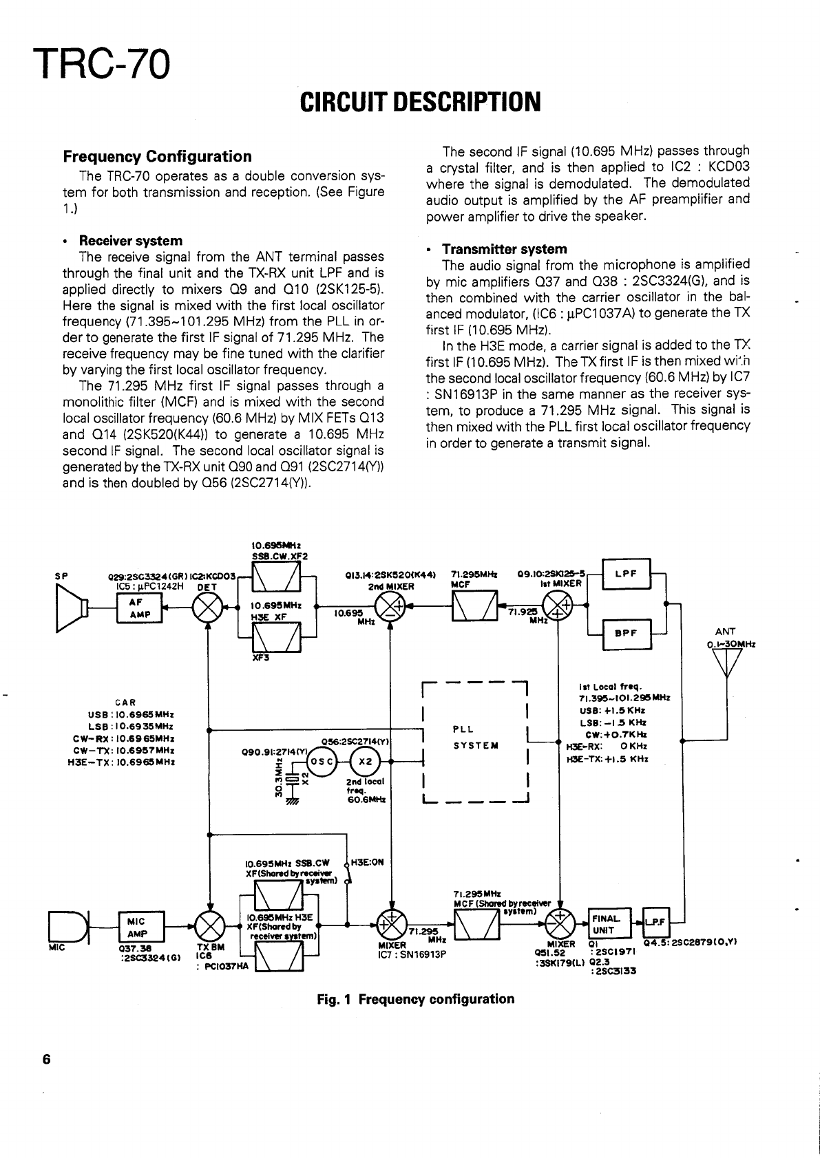
CIRCUIT
DESCRIPTION
..........cessessscscesteseneserseeserses
6
FINAL
UNIT
(X45-3370-21)
..........0csseeceereseereees
101
DESCRIPTION
OF
COMPONENTS
..........ccccseeess
27
SCHEMATIC
DIAGRAM
...........ssscsssseecerseeseeeeensees
105
PARTS
LIST
0.00...
ccseececeseeeeeeeseeseeseesnesecerseuanseentesees
33
MAT-100
(AUTOMATIC
ANTENNA
TUNER)
EXPLODED
VIEW.............:cecccsscsseussessectencecssseeeseeenes
63
Circuit
Description
........cccccccsseneceeereeeseeneneees
108
PACKING
........:.cscsesceceerceseeseserensecsereresucuarsseseesseeses
65
Block
Diagram
..........scssssscsnsssne
cecceneesenereenes
122
ADJUSTMENT
........csssscsessecsseseecercscerscesscenseevsuensass
66
Description
of
Components
.........-:cccecesseceee
123
LEVEL
DIAGRAM
...........::.scssecseessseeescencerstsseeseresees
76
Parts
List
...........-cessscsssorssessesssecessse
cnseneceserensenss
124
BLOCK
DIAGRAM
..........:ssccossscsnsssssneesessresseeeeses
77
Exploded
View
.......:..:cssscssssssesesesesssceenseeeeeees
129
TERMINAL
FUNCTION
............:ccssssssssssestssssseseeses
81
PC
Board
View
CIRCUIT
DIAGRAMS
/
PC
BOARD
VIEWS
LED
UNIT
(W02-0844-08)
...........:0ccreccceeeeees
130
LCD
ASS'Y
(B38-0324-05)
.........:cssessesseesseeerees
83
ANT
MODULE
UNIT
(W02-0883-08)
...........
131
VCO
(X58-3720-10)
.......sccsscstsssesnsenseessceeersneeses
83
Schematic
Diagram
..........ccsesseseeccccceeesneseeees
133
SIDE
TONE
(X59-1060-00)
.........c.csccsssneseesees
84
Installation
INStructiONS
..........cceeeeeeeeeneeneneees
136
DC-DC
(X59-1100-O0)
........scscssscccssesssseseeeesees
84
Manual
Tuning
.............---.:cecsseecenneneeeeeeresereees
140
FAN
&
TEMP
PROTECTION
(X59-3370-00)
.....
84
Specifications
..........ccccccssecseseseen
cnnesssecesseeeees
141
VCO
(X59-3440-00)
.......:ccssescsssesessseeeenenenecses
84
SPECIFICATIONS.
.......sccecsssssessereerersees
.
BACK
COVER