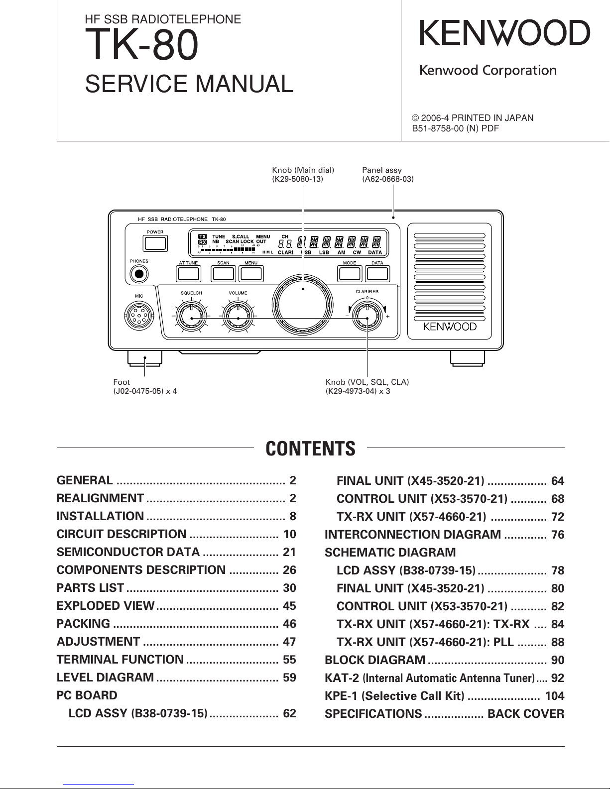
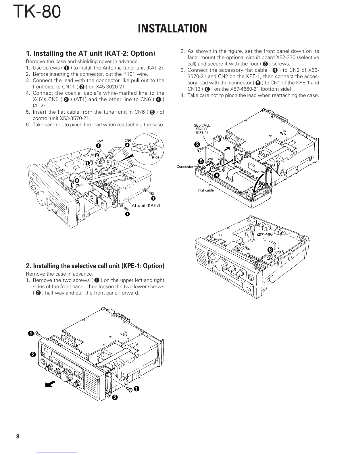
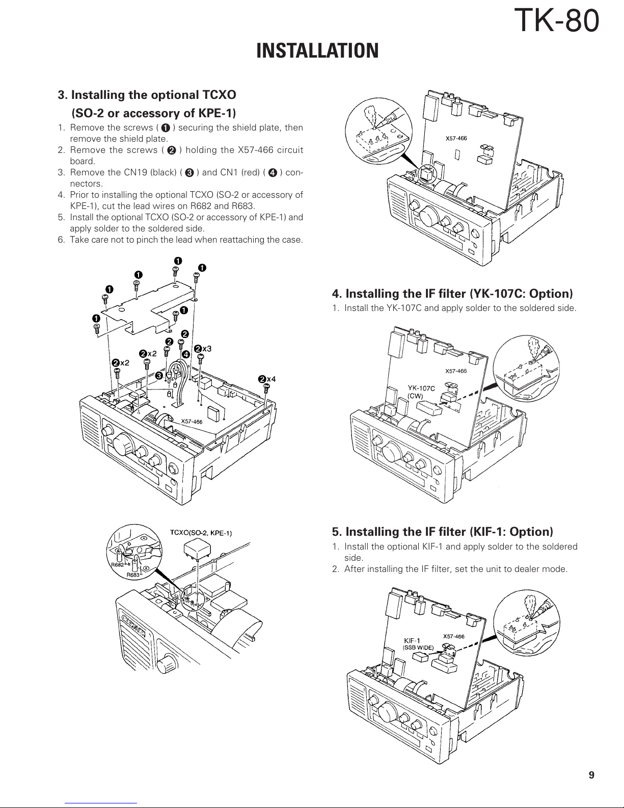
Kenwood TK-80 User manual

Document Copyrights
Copyright 2006 by Kenwood Corporation. All rights reserved.
No part of this manual may be reproduced, translated, distributed, or transmitted in any
form or by any means, electronic, mechanical, photocopying, recording, or otherwise, for
any purpose without the prior written permission of Kenwood.
Disclaimer
While every precaution has been taken in the preparation of this manual, Kenwood
assumes no responsibility for errors or omissions. Neither is any liability assumed for
damages resulting from the use of the information contained herein. Kenwood reserves
the right to make changes to any products herein at any time for improvement purposes.

© 2006-4 PRINTED IN JAPAN
B51-8758-00 (N)PDF
HF SSB RADIOTELEPHONE
TK-80
SERVICE MANUAL
Knob (Main dial)
(K29-5080-13)
Panel assy
(A62-0668-03)
Knob (VOL, SQL, CLA)
(K29-4973-04) x 3
Foot
(J02-0475-05) x 4
GENERAL ................................................... 2
REALIGNMENT .......................................... 2
INSTALLATION .......................................... 8
CIRCUIT DESCRIPTION ........................... 10
SEMICONDUCTOR DATA ....................... 21
COMPONENTS DESCRIPTION ............... 26
PARTS LIST .............................................. 30
EXPLODED VIEW..................................... 45
PACKING .................................................. 46
ADJUSTMENT ......................................... 47
TERMINAL FUNCTION ............................ 55
LEVEL DIAGRAM ..................................... 59
PC BOARD
LCD ASSY (B38-0739-15)..................... 62
FINAL UNIT (X45-3520-21) .................. 64
CONTROL UNIT (X53-3570-21) ........... 68
TX-RX UNIT (X57-4660-21) ................. 72
INTERCONNECTION DIAGRAM ............. 76
SCHEMATIC DIAGRAM
LCD ASSY (B38-0739-15)..................... 78
FINAL UNIT (X45-3520-21) .................. 80
CONTROL UNIT (X53-3570-21) ........... 82
TX-RX UNIT (X57-4660-21): TX-RX .... 84
TX-RX UNIT (X57-4660-21): PLL ......... 88
BLOCK DIAGRAM .................................... 90
KAT-2
(Internal Automatic Antenna Tuner)....
92
KPE-1 (Selective Call Kit) ...................... 104
SPECIFICATIONS .................. BACK COVER
CONTENTS

TK-80
2
GENERAL / REALIGNMENT
INTRODUCTION
SCOPE OF THIS MANUAL
This manual is intended for use by experienced techni-
cians familiar with similar types of commercial grade commu-
nications equipment. It contains all required service informa-
tion for the equipment and is current as of the publication
date. Changes which may occur after publication are covered
by either Service Bulletins or Manual Revisions, which are
issued as required.
ORDERING REPLACEMENT PARTS
When ordering replacement parts or equipment informa-
tion, the full part identification number should be included.
This applies to all parts: components, kits, or chassis. If the
part number is not known, include the chassis or kit number
of which it is a part, and a sufficient description of the re-
quired component for proper identification.
PERSONAL SAFETY
The following precautions are recommended for personal
safety:
• DO NOT transmit until all RF connectors are verified to be
secure and any open connectors are properly terminated.
•SHUT OFF and DO NOT operate this equipment near elec-
trical blasting caps or in an explosive atmosphere.
• This equipment should be serviced only by qualified tech-
nicians.
SERVICE
This radiotelephone is designed for easy servicing. Refer
to the schematic diagrams, printed circuit board views, and
alignment procedures contained within.
1. Modes
Power supply OFF
1. User mode
3. Dealer mode
2. User menu mode
4. Dealer menu mode
5. Service adjustment mode
6. Reset mode
Note:
DIP SW1 is set to “ON” when shipped from the factory. If
the dealer mode, service adjustment mode, and reset mode
fail to function, please check to see that DIP SW1 is set to
“ON”.
No. Mode Function
1User mode For normal use.
2User menu mode Selects the user menu.
3 Dealer mode Writes the various data settings to
the memory channels.
4Dealer menu mode Selects the dealer menu.
5Service adjustment Selects the adjustment items for
mode the service adjustment mode menu.
6 Reset mode Clears all memory channels and the
menu contents.

TK-80
3
2. How to Enter Each Mode
No. Mode Operation
1User mode Power ON
2User menu mode [User mode] + [MENU]
3Dealer mode [MENU] + [MODE] + Power ON
4 Dealer menu mode [Dealer mode] + [MENU]
5
Service adjustment
mode [SCAN] + [DATA] + Power ON
6Reset mode [MENU] + [MODE] + [DATA]
+ Power ON
[POWER]
key
[SCAN]
key
[MENU]
key
[MODE]
key
[DATA]
key
[DIAL]
3. Reset Mode
3-1. All Reset
Restores the factory default settings.
Set DIP SW1 to ON, then press [POWER] while holding
[MENU], [MODE], and [DATA].
“HELLO” appears on the display, indicating the system
has been reset.
• All reset does not clear adjustment data settings.
• If the power supply is cut off during all reset, the forced all
reset is executed as soon as power is restored.
3-2. Battery Reset
When the power supply from the backup battery is inter-
rupted, the factory default settings are restored, except for
memory channels 01 to 10.
• Battery reset occurs automatically whenever the power
backup fails to function.
Dealer mode enabled
Memory channel
selector write mode
DIP switch SW1 is ON.
Press [POWER] while
holding [MENU] and
[MODE].
Turn [DIAL] or
press any key.
[DATA]
[MENU]
[MODE]
[MODE]
RX frequency write
mode *2
[DATA][MODE]
TX frequency write
mode *2
[DATA][MODE]
Type of emission
(MODE) write mode *2
[DATA][MODE]
Alphanumeric display
data write mode *2
[DATA]
[DATA]
[MODE]
[MODE]
Transmit power limit
write mode
[DATA]
*1
*1
[MENU]
[MENU]
[MENU]
[MENU]
[MENU]
Dealer
menu
mode
Press [DATA]
or [MODE]
to switch
memory
channels.
Turn [DIAL]
to change
the setting.
*1 : When the specified diode D7 is not present.
*2 : Press [SCAN] to more to the next digit.
4. Dealer Mode
• This mode allows dealers to select functions for users.
• Dealers can customize the receive frequency, transmit
frequency, type of emission (MODE), alphanumeric dis-
play, transmission power limit, and set functions.
Contents to be Mode to be used Purpose
customized
Receive Receive frequency To write to memory
frequency write mode channels
Transmit Transmit frequency
frequency write mode
Type of emission Type of emission
(MODE) (MODE) write mode
Alphanumeric Alphanumeric display
display data write mode
Transmit power Transmit power limit
limit write mode
Set function Menu mode
Select function setting
-Memory channel To select memory
selector mode channels
REALIGNMENT

TK-80
4
4-1. Procedure ( ): Initial value
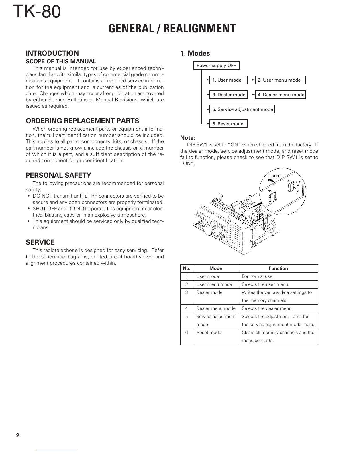
1) Press [POWER] while holding [MENU] and [MODE].
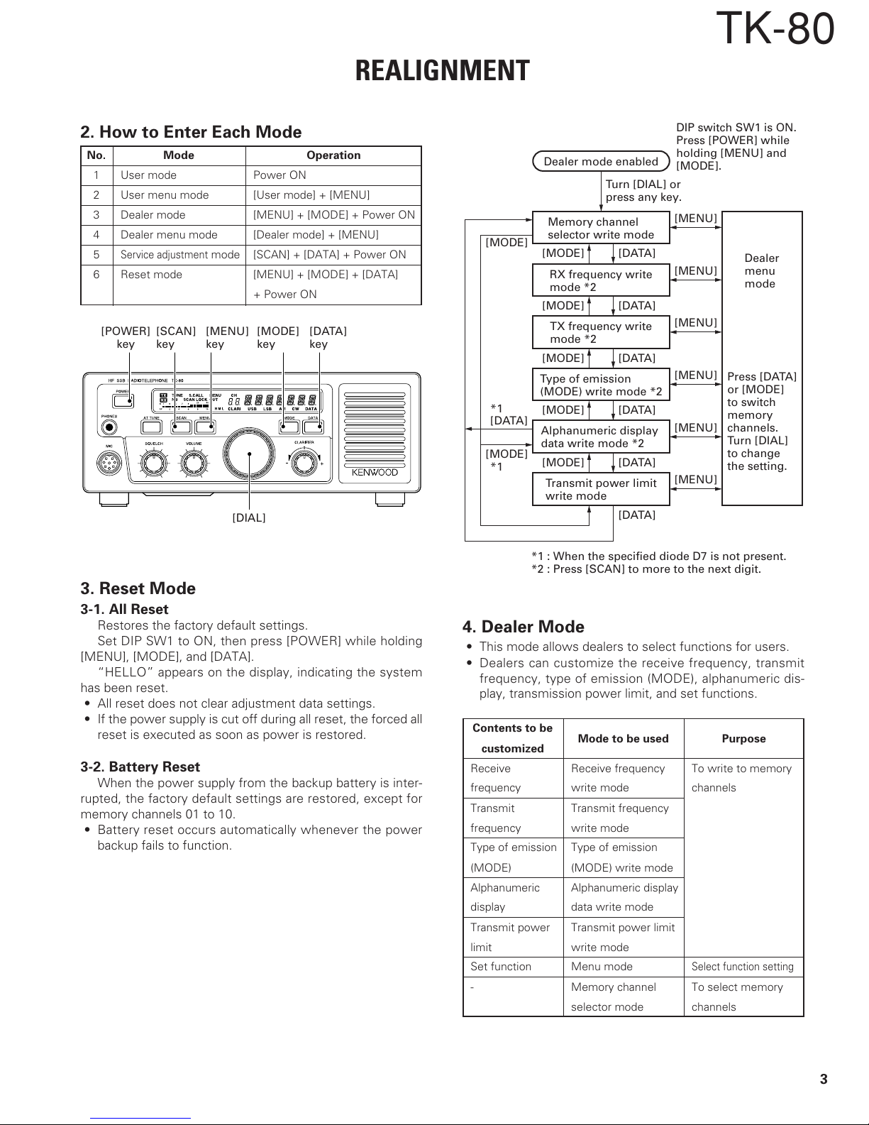
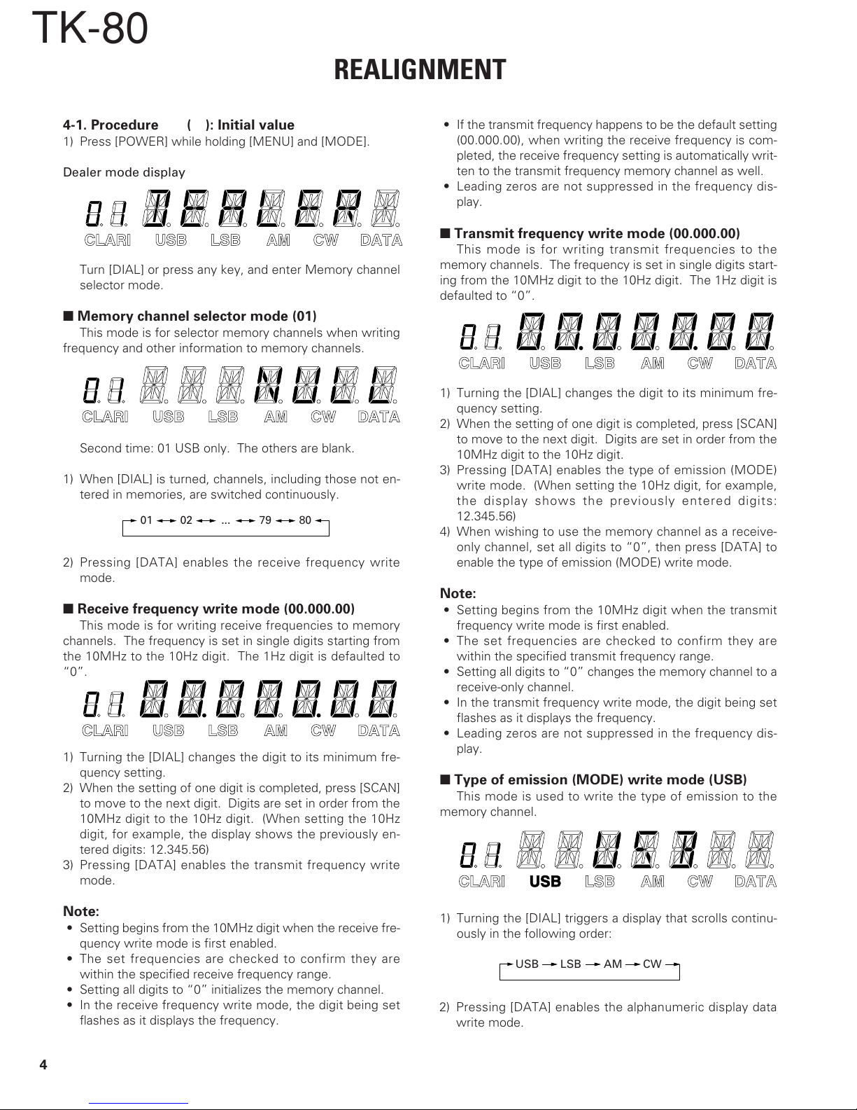
Dealer mode display
Turn [DIAL] or press any key, and enter Memory channel
selector mode.
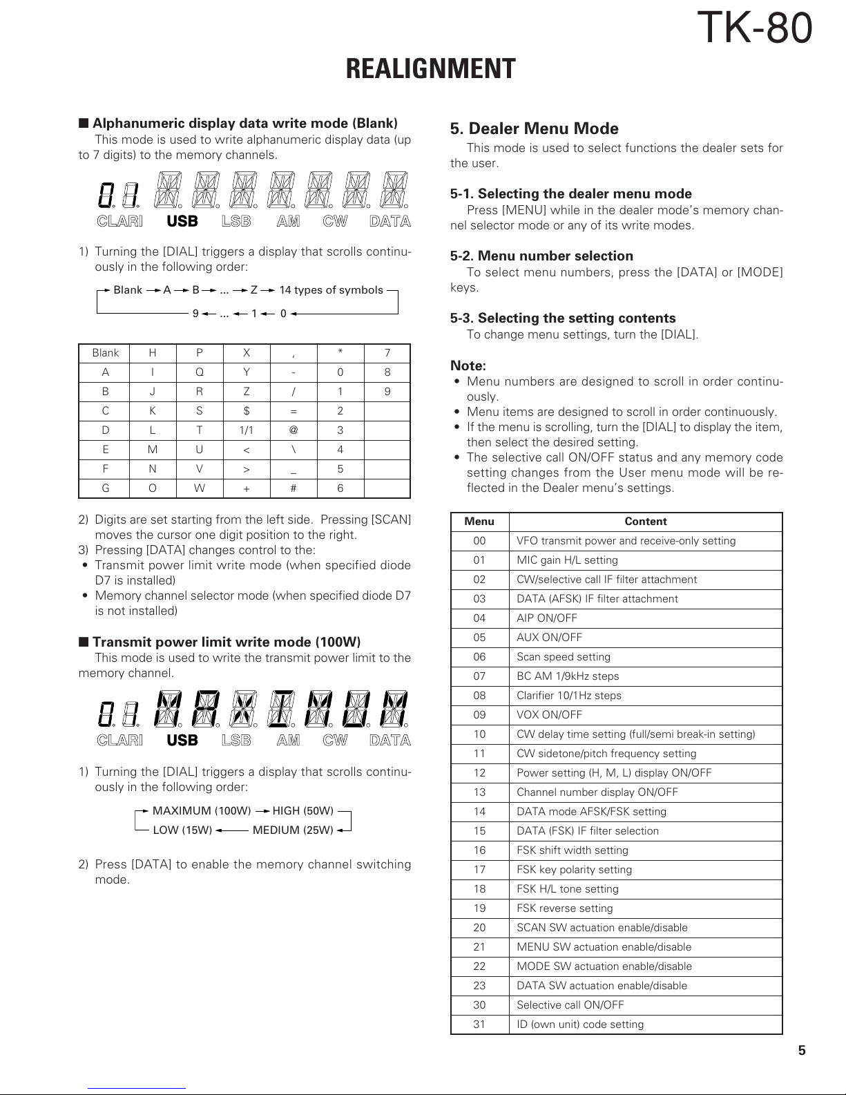
■Memory channel selector mode (01)
This mode is for selector memory channels when writing
frequency and other information to memory channels.
Second time: 01 USB only. The others are blank.
1) When [DIAL] is turned, channels, including those not en-
tered in memories, are switched continuously.
1) Turning the [DIAL] changes the digit to its minimum fre-
quency setting.
2) When the setting of one digit is completed, press [SCAN]
to move to the next digit. Digits are set in order from the
10MHz digit to the 10Hz digit. (When setting the 10Hz
digit, for example, the display shows the previously en-
tered digits: 12.345.56)
3) Pressing [DATA] enables the transmit frequency write
mode.
Note:
• Setting begins from the 10MHz digit when the receive fre-
quency write mode is first enabled.
• The set frequencies are checked to confirm they are
within the specified receive frequency range.
• Setting all digits to “0” initializes the memory channel.
• In the receive frequency write mode, the digit being set
flashes as it displays the frequency.
2) Pressing [DATA] enables the receive frequency write
mode.
■Receive frequency write mode (00.000.00)
This mode is for writing receive frequencies to memory
channels. The frequency is set in single digits starting from
the 10MHz to the 10Hz digit. The 1Hz digit is defaulted to
“0”.
01 02 79 80...
• If the transmit frequency happens to be the default setting
(00.000.00), when writing the receive frequency is com-
pleted, the receive frequency setting is automatically writ-
ten to the transmit frequency memory channel as well.
• Leading zeros are not suppressed in the frequency dis-
play.
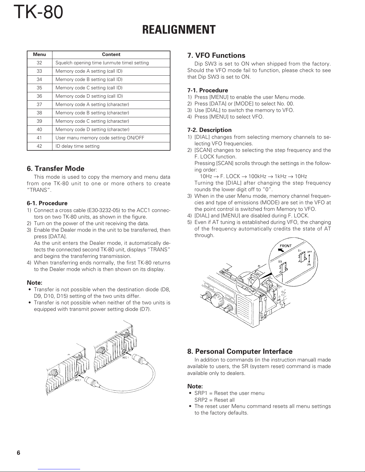
■Transmit frequency write mode (00.000.00)
This mode is for writing transmit frequencies to the
memory channels. The frequency is set in single digits start-
ing from the 10MHz digit to the 10Hz digit. The 1Hz digit is
defaulted to “0”.
1) Turning the [DIAL] changes the digit to its minimum fre-
quency setting.
2) When the setting of one digit is completed, press [SCAN]
to move to the next digit. Digits are set in order from the
10MHz digit to the 10Hz digit.
3) Pressing [DATA] enables the type of emission (MODE)
write mode. (When setting the 10Hz digit, for example,
the display shows the previously entered digits:
12.345.56)
4) When wishing to use the memory channel as a receive-
only channel, set all digits to “0”, then press [DATA] to
enable the type of emission (MODE) write mode.
Note:
• Setting begins from the 10MHz digit when the transmit
frequency write mode is first enabled.
• The set frequencies are checked to confirm they are
within the specified transmit frequency range.
• Setting all digits to “0” changes the memory channel to a
receive-only channel.
• In the transmit frequency write mode, the digit being set
flashes as it displays the frequency.
• Leading zeros are not suppressed in the frequency dis-
play.
■Type of emission (MODE) write mode (USB)
This mode is used to write the type of emission to the
memory channel.
1) Turning the [DIAL] triggers a display that scrolls continu-
ously in the following order:
2) Pressing [DATA] enables the alphanumeric display data
write mode.
USB LSB AM CW
REALIGNMENT

TK-80
5
■Alphanumeric display data write mode (Blank)
This mode is used to write alphanumeric display data (up
to 7 digits) to the memory channels.
1) Turning the [DIAL] triggers a display that scrolls continu-
ously in the following order:
Blank A B Z 14 types of symbols...
910...
Blank H P X , * 7
AIQY-08
BJRZ / 19
CKS$=2
DLT1/1 @ 3
EMU< \ 4
FNV>_5
GOW+ # 6
2) Digits are set starting from the left side. Pressing [SCAN]
moves the cursor one digit position to the right.
3) Pressing [DATA] changes control to the:
• Transmit power limit write mode (when specified diode
D7 is installed)
• Memory channel selector mode (when specified diode D7
is not installed)
■Transmit power limit write mode (100W)
This mode is used to write the transmit power limit to the
memory channel.
1) Turning the [DIAL] triggers a display that scrolls continu-
ously in the following order:
MAXIMUM (100W) HIGH (50W)
MEDIUM (25W)LOW (15W)
2) Press [DATA] to enable the memory channel switching
mode.
5. Dealer Menu Mode
This mode is used to select functions the dealer sets for
the user.
5-1. Selecting the dealer menu mode
Press [MENU] while in the dealer mode’s memory chan-
nel selector mode or any of its write modes.
5-2. Menu number selection
To select menu numbers, press the [DATA] or [MODE]
keys.
5-3. Selecting the setting contents
To change menu settings, turn the [DIAL].
Note:
• Menu numbers are designed to scroll in order continu-
ously.
• Menu items are designed to scroll in order continuously.
• If the menu is scrolling, turn the [DIAL] to display the item,
then select the desired setting.
• The selective call ON/OFF status and any memory code
setting changes from the User menu mode will be re-
flected in the Dealer menu’s settings.
Menu Content
00 VFO transmit power and receive-only setting
01 MIC gain H/L setting
02 CW/selective call IF filter attachment
03 DATA (AFSK) IF filter attachment
04 AIP ON/OFF
05 AUX ON/OFF
06 Scan speed setting
07 BC AM 1/9kHz steps
08 Clarifier 10/1Hz steps
09 VOX ON/OFF
10 CW delay time setting (full/semi break-in setting)
11 CW sidetone/pitch frequency setting
12 Power setting (H, M, L) display ON/OFF
13 Channel number display ON/OFF
14 DATA mode AFSK/FSK setting
15 DATA (FSK) IF filter selection
16 FSK shift width setting
17 FSK key polarity setting
18 FSK H/L tone setting
19 FSK reverse setting
20 SCAN SW actuation enable/disable
21 MENU SW actuation enable/disable
22 MODE SW actuation enable/disable
23 DATA SW actuation enable/disable
30 Selective call ON/OFF
31 ID (own unit) code setting
REALIGNMENT

TK-80
6
Menu Content
32 Squelch opening time (unmute time) setting
33 Memory code A setting (call ID)
34 Memory code B setting (call ID)
35 Memory code C setting (call ID)
36 Memory code D setting (call ID)
37 Memory code A setting (character)
38 Memory code B setting (character)
39 Memory code C setting (character)
40 Memory code D setting (character)
41 User manu memory code setting ON/OFF
42 ID delay time setting
6. Transfer Mode
This mode is used to copy the memory and menu data
from one TK-80 unit to one or more others to create
“TRANS”.
6-1. Procedure
1) Connect a cross cable (E30-3232-05) to the ACC1 connec-
tors on two TK-80 units, as shown in the figure.
2) Turn on the power of the unit receiving the data.
3) Enable the Dealer mode in the unit to be transferred, then
press [DATA].
As the unit enters the Dealer mode, it automatically de-
tects the connected second TK-80 unit, displays “TRANS”
and begins the transferring transmission.
4) When transferring ends normally, the first TK-80 returns
to the Dealer mode which is then shown on its display.
Note:
• Transfer is not possible when the destination diode (D8,
D9, D10, D15) setting of the two units differ.
• Transfer is not possible when neither of the two units is
equipped with transmit power setting diode (D7).
7. VFO Functions
Dip SW3 is set to ON when shipped from the factory.
Should the VFO mode fail to function, please check to see
that Dip SW3 is set to ON.
7-1. Procedure
1) Press [MENU] to enable the user Menu mode.
2) Press [DATA] or [MODE] to select No. 00.
3) Use [DIAL] to switch the memory to VFO.
4) Press [MENU] to select VFO.
7-2. Description
1) [DIAL] changes from selecting memory channels to se-
lecting VFO frequencies.
2) [SCAN] changes to selecting the step frequency and the
F. LOCK function.
Pressing [SCAN] scrolls through the settings in the follow-
ing order:
10Hz →F. LOCK →100kHz →1kHz →10Hz
Turning the [DIAL] after changing the step frequency
rounds the lower digit off to “0”.
3) When in the user Menu mode, memory channel frequen-
cies and type of emissions (MODE) are set in the VFO at
the point control is switched from Memory to VFO.
4) [DIAL] and [MENU] are disabled during F. LOCK.
5) Even if AT tuning is established during VFO, the changing
of the frequency automatically credits the state of AT
through.
8. Personal Computer Interface
In addition to commands (in the instruction manual) made
available to users, the SR (system reset) command is made
available only to dealers.
Note:
• SRP1 = Reset the user menu
SRP2 = Reset all
• The reset user Menu command resets all menu settings
to the factory defaults.
REALIGNMENT

TK-80
7
9. User Menu Mode
This mode enables users to select various settings to suit
their individual needs. The items that can be modified are
listed below:
Menu Content
00 VFO/M
01 Transmit power switching
02 NB ON/OFF
03 Display switching frequency/alphanumeric
04 LOCK OUT ON/OFF
05 Scan busy stop switching TO/CO/OFF
06 Selective call ON/OFF
07 ID (own unit) code display
08 Memory code A setting (call ID)
09 Memory code B setting (call ID)
10 Memory code C setting (call ID)
11 Memory code D setting (call ID)
12 Memory code A setting (character)
13 Memory code B setting (character)
14 Memory code C setting (character)
15 Memory code D setting (character)
REALIGNMENT
9-1. Selecting settings
• Begin by pressing [MENU] to display the User menu.
• Press [MODE] or [DATA] to select the desired item num-
ber.
• Use [DIAL] to change the setting.
• Press [MENU] once more to complete the change.
Note:
• Menu numbers are designed to scroll in order continu-
ously.
• Menu items are designed to scroll in order continuously.
• Menu item number “00” can only be set when DIP SW3 is
set to ON.
• Menu item numbers 08 to 15 can only be set when the
user memory code setting in the Dealer menu mode is set
to ON.
• Menu item numbers 01 and 04 represent the channels
prior to entering the user menu mode.
• If a Selective call kit is not installed, setting item number 06
(user’s own office code) to ON will only produce on the
display. The selective call mode will not be enabled.
• Switching the [MENU] key ON/OFF can be inhibited from
the Dealer menu mode.

TK-80
8
1. Installing the AT unit (KAT-2: Option)
Remove the case and shielding cover in advance.
1. Use screws ( ➊) to install the Antenna tuner unit (KAT-2).
2. Before inserting the connector, cut the R101 wire.
3. Connect the lead with the connector like pull out to the
front side to CN11 ( ➋) on X45-3620-21.
4. Connect the coaxial cable’s white-marked line to the
X45’s CN5 ( ➌) (AT1) and the other line to CN6 ( ➍)
(AT2).
5. Insert the flat cable from the tuner unit in CN6 ( ➎) of
control unit X53-3570-21.
6. Take care not to pinch the lead when reattaching the case.
2.
Installing the selective call unit (KPE-1: Option)
Remove the case in advance.
1. Remove the two screws ( ➊) on the upper left and right
sides of the front panel, then loosen the two lower screws
(➋) half way and pull the front panel forward.
2. As shown in the figure, set the front panel down on its
face, mount the optional circuit board X52-330 (selective
call) and secure it with the four ( ➌) screws.
3. Connect the accessory flat cable ( ➍) to CN2 of X53-
3570-21 and CN2 on the KPE-1, then connect the acces-
sory lead with the connector ( ➎) to CN1 of the KPE-1 and
CN13 ( ➏) on the X57-4660-21 (bottom side).
4. Take care not to pinch the lead when reattaching the case.
INSTALLATION

TK-80
9
INSTALLATION
4. Installing the IF filter (YK-107C: Option)
1. Install the YK-107C and apply solder to the soldered side.
5. Installing the IF filter (KIF-1: Option)
1. Install the optional KIF-1 and apply solder to the soldered
side.
2. After installing the IF filter, set the unit to dealer mode.
3. Installing the optional TCXO
(SO-2 or accessory of KPE-1)
1. Remove the screws ( ➊) securing the shield plate, then
remove the shield plate.
2. Remove the screws ( ➋) holding the X57-466 circuit
board.
3. Remove the CN19 (black) ( ➌) and CN1 (red) ( ➍) con-
nectors.
4. Prior to installing the optional TCXO (SO-2 or accessory of
KPE-1), cut the lead wires on R682 and R683.
5. Install the optional TCXO (SO-2 or accessory of KPE-1) and
apply solder to the soldered side.
6. Take care not to pinch the lead when reattaching the case.

TK-80
10
CIRCUIT DESCRIPTION
1. Frequency Configuration
The TK-80 uses double conversion in all modes.
Mode Display frequency
USB/LSB Carrier point frequency
CW Transmission carrier frequency
AM Transmission carrier frequency
FSK Mark transmission frequency
AFSK Carrier point frequency
Table 1 Display frequency in each mode
The receiver frequency in SSB mode is given by the fol-
lowing equation when the receiver tone produced by the in-
put frequency (fIN) from the antenna is zero beat (when an
SSB signal with a carrier point of fIN is zeroed in):
fIN = fLO1 – fLO2 – fCAR .................... (1)
73.045MHz
TX MIX-2
RX MIX-1
TX MIX-1
RX MIX-2
B.M
DET
ANT
10.695MHz
73.045MHz
MIC IN
AF OUT
fin
LO1 LO2 CAR
73.145~
103.045MHz
62.35MHz 10.695MHz
Since all these frequencies are generated by the PLL cir-
cuit, as shown in Figure 2 (PLL circuit frequency configura-
tion), the receiver frequency is determined only by the refer-
ence frequency, fSTD, and the PLL divide ratio. This means
the accuracy of the reference frequency determines the ac-
curacy of the operating frequency of the transceiver.
The accuracy of the reference crystal oscillator used in the
TK-80 is 10ppm (–10°C to +50°C). The accuracy of the op-
tional temperature-compensated crystal oscillator (TCXO SO-
2) is 0.5ppm (–10°C to +50°C).
In SSB transmission mode or in other modes, the fre-
quency is determined by the reference frequency (fSTD and
the PLL divide ratio). Table 1 lists the display frequencies in
the various modes.
The pitch of the incoming signal in CW mode can be varied
in 50Hz steps in the range of 400 or 800Hz without changing
the center frequency of the IF filter (variable CW pitch sys-
tem).
2. PLL Circuit Configuration
The TK-80 PLL circuit uses a reference frequency of
20MHz, and covers 100kHz to 30MHz. Figure 2 shows a PLL
block diagram and frequency configurations.
2-1. Reference oscillator circuit
The reference frequency (fSTD) for frequency control is
generated by the 20MHz crystal oscillator, X501 and Q525.
The 20MHz reference frequency is supplied to DDS IC500
and IC501 and PLL IC502.
The crystal oscillator circuit can be replaced by an optional
TCXO (SO-2 or accessory of KPE-1). The TK-80 can be
switched to the TCXO by removing resistors R682 and R683.
2-2. LO1 (PLL loop)
Q531, Q533, and Q535 are VCOs.
Q531 (VCO1) generates a signal of 73.145 to 83.544MHz.
Q533 (VCO2) generates a signal of 83.545 to 94.544MHz.
Q535 (VCO3) generates a signal of 94.545 to 103.045MHz.
The 20MHz reference signal of fSTD is input to pin 15 of
IC502 and is divided by 40 to produce a 500kHz comparison
frequency. The output signal from the VCO is mixed with a
53.545 to 54.045MHz signal from the PLL (described later)
and IC503 (Mixer) to produce a 19.5 to 49.5MHz signal. It is
then input to pin 6 of IC502, divided, and compared with the
500kHz signal by the phase comparator. The VCO frequency
is then locked. The divide ratio date is supplied by the digital
unit.
At IC500, a 1.195 to 1.695MHz digital signal is generated
and the CP500, CP501 ladder resistor and Q522 D/A con-
verter are used to convert it into an analog signal. That signal
is put through a low-pass filter and mixed with 10MHz at
mixer IC504 to produce 8.305 to 8.805MHz.
Furthermore, 62.35MHz oscillated by X502 and Q517 is
mixed at mixer IC505 to become the above mentioned
53.545 to 54.045MHz signal.
Fig. 1 Frequency configuration

TK-80
11
2-3. LO2 (PLL loop)
The part oscillated by X502 and Q517 is output to LO1
cancel loop after passing through the Q518 buffer and input
into mixer IC505. The other part is output from CN502 as
LO2.
2-4. CAR
A digital signal is generated near 695kHz at IC501, and the
analog signal converted by the CP502, CP503 ladder resis-
tors and Q522 D/A converter are mixed with the 10MHz gen-
erated from the chop output of IC501 at IC506. This is then
output as 10.695MHz through the band-pass filter and the
amplifier.
During receiving AM mode, the DDS oscillation is
stopped. In FSK mode, the internal register of IC501 is
switched for direct FSK modulation by the external RTK sig-
nal during selective call mode code transmission by the ABSL
signal from the CPU.
2-5. DDS circuit configuration
The DDS IC has been developed with standard cells to
implement a high-speed circuit and large-capacity ROM at
low cost.
Q526
2SC2714(Y)
Q525
2SC2714(Y)
Q514
2SC2712(GR)
20MHz
Q527
2SC2996(Y)
Q529
2SC2712(Y)
Q528
2SC2996(Y)
Q536
2SC2714(Y)
Q507
2SC2714(Y)
Rin 1/40 PD
1/N
15
IC502
MB86001PF
SO-2
OSC
OPTION
DO2
9
Fin
6
Q508~510
2SC3722K(R)
A. LPF
BPF
LPF
LPF
LPF
BPFDDS1
LPF
VCO2
VCO3
VCO1
Q511
2SC2714(Y)
Q512
2SC2712(Y)
Q515
2SC2712(Y)
Q523
2SC2712(Y)
Q516
2SC2712(Y)
Q513
2SC2714(Y)
19.5~
49.5MHz
BPF
53.545~
54.045MHz
LO1
: 73.145~
103.045MHz
3.4dBm
LO2
: 62.35MHz
2.5dBm
CAR
: 10.695MHz
–1.2dBm
IC503
NJM2594V
+
+
+
+
–
–+
–
Q531,533,535
2SK508NV(K52)
PLL
IC500
F71022Z
CF500
Q522
2SC2712(GR)
DDS2
IC501
F71022Z
695kHz+∆
IC504
NJM2594V
IC506
NJM2594V
IC505
UPC1686G
8.305~
8.805MHz
Q519
2SC2714(Y)
Q518
2SC2714(Y)
Q520
2SC2714(Y)
Q524
2SC2714(Y)
Q521
2SC2714(Y)
OSC
Q517
2SC2714(Y)
62.35MHz
1.195~
1.695MHz
CHOP
10MHz
10.695MHz
N=39~99
VCO1: 73.145~83.544MHz
VCO2: 83.545~94.544MHz
VCO3: 94.545~103.045MHz
■IC configuration
IC configuration is as follows:
• There are two 28 bit registers for setting frequency data,
one 28 bit frequency shift register for addition to the fre-
quency registers, a 23 bit parallel signal input section for
frequency modulation with parallel signals, and a data en-
try and selection section.
• There is a frequency-modulation section comprising 28 bit
adders for adding frequency data and frequency modula-
tion data, a phase data operation section that adds data
from the frequency modulation section and 28 bit phase
data register, and a SIN-ROM that converts phase data to
sine waves.
■Frequency/shift data setting
Using serial signals synchronized with clock pulses, 30
bits (2 bits that specify the destination for which data is set,
and 28 bits of frequency data) are set in the three internal
registers.
■Frequency register selection
The data set in the two frequency registers is selected by
the SLAB input of the DDS IC. This pin handles the ABSL
signal for IC501, and the CASL signal for IC500. This function
eliminates the need for the TK-80 to set frequency data for
each transmission/reception with the microprocessor.
Fig. 2 PLL block diagram and frequency configuration
CIRCUIT DESCRIPTION

TK-80
12
■Frequency data selection
The SPSL input of the DDS IC selects whether to use the
data in the internal frequency shift register or the data from
the parallel input as frequency modulation data.
■Frequency modulation
The MDEN input of the DDS IC enables or disables fre-
quency modulation. When frequency modulation is enabled,
frequency data is added, and the result is input to the phase
data operation section.
■Phase data operation
The target frequency phase data is output by accumulat-
ing 28 bit frequency data in the 28-bit phase accumulator.
FOUT = Fs/228 x Dsum
Fs: DDS IC input frequency/2
Dsum: Frequency data + Frequency modulation data
If 225 is set for Dsum when 1/8 Fs is output, the phase data
must be increased by π/8.
So far, 28 bit absolute value operation has been used, but
a 28 bit signed operation can also be used, assuming that the
MSB is a sign. If complement data of 8000000 to FFFFFFFF
(hex) is set, the phase moves in the negative direction for
positive data.
■SIN-ROM
Phase data from the phase data operation section is con-
verted to sine wave data of 0000 to FFFF (hex) in 16 bit offset
binary format (Fig. 3).
2π= 2
28
7π/8 = –2
25
π/8 = 2
25
FFFFH
0000H
Fig. 3
1.605~2.5MHz
ANT
RX
TX ~30MHz ~30MHz
~30MHz
D6
D8 D5D7
D9 D10
D23 D24
D25 D26
2.5~4.5MHz
D11 D12
4.5~8.0MHz
D13 D14
8.0~10.5MHz
D15 D16
10.5~14.5MHz
D17 D18
14.5~21.5MHz
D19 D20
21.5~30MHz
D21
D51
D22 D50
1.605MHz~ ~1.605MHz
Q8,9
AIP ON
AIP OFF
1st MIX
Q4~7
IF
LO1
73.145~
103.045MHz
FINAL UNIT (X45-3520-21) TX-RX UNIT (X57-4660-21)
3. Receiver Circuit Configuration
The configuration of the receiver circuit is double conver-
sion with a first IF of 73.045MHz and a second IF of 10.695
MHz in SSB, AM, CW mode.
The incoming signal from the antenna passes through the
antenna switch relay of the final unit, then through the 30
MHz low-pass filter, and goes to the TX-RX unit. The signal
passes through a 30MHz low-pass filter in the TX-RX unit,
and goes through the 8-segmented band-pass filters. If AIP
is off, the signal passing through band-pass filter is amplified
by the RF amplifier, Q8, Q9, and is input to the first mixer, Q4
to Q7. If AIP is on, the signal bypasses Q8 and Q9 and goes
directly to the first mixer. It is mixed with the LO1 signal by
the first mixer to produce a first IF signal of 73.045MHz.
Fig. 4 Receiver front-end
CIRCUIT DESCRIPTION

TK-80
13
Q18
TH1
Q19 L51
Q20
SW
2nd IF
NBI
NBG
W1
TP801
L802 L803
Q802
Q801
NBS
Q800 +
+
Q803 Q805
Q807
Q808
D800
Q806
Q804
Noise
AMP
+
RXB
AGC
8F
8A
to IF filter
RBK
The first IF signal of 73.045MHz passes through the MCF
(XF1), is amplified by the IF amplifier Q10, and mixed with the
62.35MHz LO2 signal by the second mixer, Q11 and Q12, to
produce a second IF signal of 10.695MHz.
The second IF signal of 10.695MHz is split into two. One
signal goes to the NB amplifier and the other passes through
the NB gate FET Q19. The signal then goes to the IF filter.
There are four types of IF filters: 6kHz, 2.7kHz, 2.2kHz, and
500Hz (2.7kHz and 500Hz are optional). The signal passing
through the IF filter is amplified Q21 and Q30, Q31 SSB, CW,
FSK modes are product-detected in D52, D53 and AM mode
envelope-detected in D54 and condenser.
After detection, the AF signal for each mode passes
through analog switch IC3 and goes to AF preamplifier Q48.
After the preamplifier, the signal passes through the mute
circuit Q49 has the volume controlled at IC6 and is amplified
to the necessary electric power level at AF power amplifier
IC7.
3-1. Receiver front-end
The signal input to the TX-RX unit passes through the 30
MHz low-pass filter, and signal above 1.605MHz goes to
seven band-pass filters. When AIP is off, the signal passes
through each band-pass filter, D25 and D26 turn on and D23
and D24 turn off, and the signal is amplified by about 13dB by
Q8, Q9 and output to the first mixer. If AIP is on, D25 and
D26 turn off and D23 and D24 turn on, and the signal is out-
put directly to the first mixer without passing through Q8 and
Q9. The first mixer is a quad balanced mixer, Q4 to Q7 (Fig.
4).
3-2. Noise blanker circuit
The 10.695MHz IF signal generated from the first IF of
73.045MHz by the second mixer is input to the IF amplifier
Q19, sent through Q18 amplified by noise amplifier Q801,
Q802 and Q804, sent through buffer Q806 and noise-de-
tected by D800. This signal switches Q805 and Q807, Q808
and controls Q19 in the TX-RX unit. Q19 controls Q20 and
blanks the noise (Fig. 5).
Fig. 5 Noise blanker circuit
CIRCUIT DESCRIPTION

TK-80
14
3-3. Signal strength meter circuit
In all mode, the signal strength meter circuit comprises
operational amplifier IC2. The signal level detected is input to
pin 3 of IC2 (1/2) and amplified by about 8dB by IC2 (2/2), then
goes to IC5 of the control unit (Fig. 6).
3-4. AGC circuit
The time constant for the signal envelope detected by IC1
is changed in each mode by the analog switch. The effective
value, not the peak value, is used in AM mode (Fig. 6).
3-5. Squelch
The squelch volume voltage is input to A/D input pin 78 of
the CPU IC5. The signal strength meter voltage made by
squelch volume voltage and the TX-RX unit is compare pro-
cessed in the CPU, controlling the ABK signal.
3-6. IF filter
There are two internal 10.695MHz IF filters and two op-
tional, so a total of four can be installed.
10.695MHz Part No./ Selection of each mode
filter name CW SSB AM DATA DATA
(AFSK) (FSK)
AM L71-0433-15 - - --
SSB-WIDE L71-0457-05 ---✳✳
(Option) /KIF-1
SSB L71-0249-05 -
CW L71-0283-15 ✳---✳
(Option) /YK-107C
represents the initial set value
✳represents selections which can be used when the op-
tional filter is attached
DATA (AFSK): SSB+DATA display
DATA (FSK): DATA display
Also, filter selection and DATA key settings are switched
in the following dealer mode menu.
CH.02: CW FILTER OUT/IN
CH.03:
DATA (AFSK)-SSB WIDE FILTER
OUT/IN
CH.15: DATA (FSK)-IF FILTER FOR SSB/SSB-W/AM/CW
CH.14: DATA MODE AFSK/FSK
Q35
Q30
D55 D54
Q33
Q31
Q38
D53
D52
L76
TH6
VR4
AGC
L75
8V
RXC
SSB, AM, CW
2nd IF IN
2
3
–
+
–
+
17
IC2 (1/2) IC2 (2/2)
6
5
VR6
+
+
+
+
+
10
11
9
8
12 6
IC1
AGS AMB SM
Contorl unit
CAR
10.695MHz
Detector
OUT
Fig. 6 S-meter and AGC circuits
CIRCUIT DESCRIPTION

TK-80
15
Item Rating
Center frequency (fo) 73.045MHz
Pass bandwidth ±7.5kHz or more at 3dB
Attenuation bandwidth ±30kHz or less at 20dB
Ripple 1dB or less
Insertion loss 2dB or less
Guaranteed attenuation 40dB or more at fo–910kHz
Terminal impedance 2kΩ±10% // L type
Temperature range –30°C~+70°C
Table 2 MCF (XF1) (L71-0432-05)
Item Rating
Nominal center frequency (fo) 10.695MHz
Pass bandwidth 6kHz or more at 6dB
Attenuation bandwidth 40kHz or less at 60dB
Ripple 2dB or less
Insertion loss 3dB or less
Guaranteed attenuation 60dB or more within fo±1MHz
Terminal impedance 1.2kΩ±10% // 6pF±10%
Table 3 MCF (XF3) (L71-0433-15)
Item Rating
Nominal center frequency (fo) 10.695MHz
Center frequency deviation Within ±200Hz at 6dB
Pass bandwidth and Width 2.75kHz or more at 6dB
Attenuation bandwidth ±2.2kHz or less at 20dB
±3.1kHz or less at 60dB
Ripple 2dB or less
Insertion loss 6dB or less
Terminal impedance 1.2kΩ±5% // 8pF±10%
Temperature range –10°C~+60°C
Table 4 MCF (L71-0457-05) KIF-1: SSB WIDE (Option)
Item Rating
Nominal center frequency (fo) 10.695MHz
Center frequency deviation Within ±200Hz at 6dB
Pass bandwidth and 2.2kHz or more at 6dB
Attenuation bandwidth ±1.5kHz or less at 20dB
±2.4kHz or less at 60dB
Ripple 2dB or less
Insertion loss 5dB or less
Guaranteed attenuation 60dB or more within fo±40kHz
Terminal impedance 1.2kΩ±5% // 6pF±5%
Table 5 MCF (XF2) (L71-0249-05)
Item Rating
Nominal center frequency (fo) 10.695MHz
Center frequency deviation Within ±80Hz (25°C, 6dB)
Pass bandwidth 500Hz or more (6dB)
Insertion loss 5dB±2dB
Terminal impedance 1200Ω// 6pF
Table 6 MCF (L71-0283-15) YK-107C: CW (Option)
4. Transmitter Circuit Configuration
The audio signal from the microphone enters CN 12 of the
TX-RX unit. The signal then goes to IC9, the microphone
amplifier. After amplifying part of IC9’s output at Q54, it is
detected by D59 and applied to the ALC terminal of IC9. The
signal gain is properly adjusted by the D/A converter IC13 and
passes through analog switch IC8, is amplified by Q50. The
amplified signal is balance-modulated with the CAR signal
(10.695MHz) input from CN9 by IC4 passed through Q51,
and sent to the crystal filter passing through the filter, is am-
plified by Q24. The signal is CAR level adjusted by the D48
pin diode, and input to the mixer.
The 62.35MHz LO2 signal from the PLL unit is input from
CN3 of the TX-RX unit, and mixed with the 10.695MHz signal
which CAR level adjusted amplified by Q25 and Q26 to pro-
duce a 73.045MHz signal. The LO1 signal from the PLL unit
is input from CN2 of the TX-RX unit, and mixed with the
73.045MHz signal passes through LC three-stage filter by
Q27 and Q28 to generate the desired signal. The signal
passes through the band-pass filter and is amplified by Q29
to produce the drive output, which goes to the final unit from
CN19.
The signal is amplified to about 100W by Q1, Q2, Q3 and
Q5, Q6. Harmonic components are attenuated by the filter
unit and the signal is output from the antenna connector.
In AM mode, the signal is generated by unbalancing the
carrier of SSB balance modulator IC4.
In CW mode, the signal is input to IC5 of the control unit.
The sidetone monitor signal is generated by IC5, and ampli-
fied by audio amplifier Q79 and IC7, and output from the
speaker. The CW control signal is output from IC5 of the
control unit, and input to CN14 of the TX-RX unit to switch
Q25 and Q26 and generate the CW signal.
4-1. ALC circuit
The forward wave voltage detected in the final unit passes
through CN15 in the TX-RX unit, its level is potential dividing
and it is applied to the differential amplifier comprising Q60
and Q61. When VSF is applied to the base of Q60, the emit-
ter voltage of Q60 and Q61 increases and the current flowing
through the base of Q61 decreases; thus the collector volt-
age rises. When this voltage exceeds the emitter voltage of
Q62 (about 1.8V) plus VBE (about 0.6V), the current flows
through the base of Q62 and the collector voltage drops.
ALC time constants C and R are connected to this collector.
The collector voltage change is shifted by Q64 and D68
(3.6V), and matched with the voltage for keying by Q65 and
D69 to generate the ALC voltage. This ALC voltage activates
ALC by lowering the second gate voltage of Q24 of the TX-RX
unit (Fig. 7).
CIRCUIT DESCRIPTION

TK-80
16
4-2. Power control circuit
Power is controlled by lowering the base voltage of Q61 in
the TX-RX unit. As the base voltage of Q61 decreases, the
emitter voltage of Q60 and Q61 decreases. This activates
ALC and reduces the power even if the base voltage (VSF) of
Q60 is low. The power change is shifted by D/A converter
IC13 for changing base voltage of Q61 (Fig. 7).
4-3. Protection circuit
When the reflected wave voltage (VSR) detected by the
filter unit rises, Q63 in TX-RX unit turns on to reduce the volt-
age of the ALC time constant line. The drive is decreased
and the power is reduced to protect the final transistor.
8F
+
Q64
Q60 Q61
Q62
Q65
D69
D68
D67
D71
D72
VR14
+
+
+
VSF
VSR
Ext ALC
D70
+
Q63
VR12
ALC out
–6V
TXB
Q69
Q67 Q68
AMB
IC13
D/A
3
POC
Fig. 7 ALC and power control circuits
5. Digital Control Circuit
The TK-80’s digital control circuit comprises a 16-bit micro-
computer CPU IC5, a reset IC3, an EEPROM IC6. Expander I/
O IC7 since there are many control signals for TX-RX unit and
filter unit, they are output to the shift register (serial to parallel
converter) in series (Fig. 8).
5-1. Power switch
With this transceiver, the power is turned on and off by
the microcomputer. When the power switch is pressed, the
microcomputer detects it and energizes, the power relay to
supply 14V to the transceiver. When the power switch is
pressed to turn the transceiver off, the microcomputer
checks it a little longer than when turning the power on and
de-energizes the power relay.
CIRCUIT DESCRIPTION
4-4. Temperature protection
If the final heat sink temperature rises, Q9 in the final unit
turns on and the fan starts running at low speed and during
transmission Q10 turns on and starts running a high speed if
the final heat sink temperature rises further.
If this is not enough to prevent the temperature from con-
tinuing to rise, the control unit CPU IC5 temperature detec-
tion port THP becomes “H”, forcibly lowering the RF output.
Also, if there are any fan troubles or if something happens to
get entangled and prevents the fan from turning, the RF out-
put is similarly forced down to prevent overheating.

TK-80
17
LCD
driver
EEPROM
IC6
Buffer
IC8
Buffer
Q3~Q6
IF-232C Outside
AT
DTMF
MIC SW
DTMF
decoder
IC3
Selective
call
decoder
IC1,IC2
LCD
Power
SW VR Buffer
Rotary
encoder
SW
AT, SCAN
MENU
MODE
DATA
SQL
CLARI
Expand
I/O
IC7
Slide
SW
Reset
IC3
Low voltage
detection
D4,D5,Q1,Q2
S1,S3
D7~D9
D12~D15
DATA BUS
Enable
VCO select
Internal AT control
Outside AT control
uart rx
reset
int
int a/d a/dtimer
(int)
timer
(PWM)
Internal
AT
AT UNIT
LCD ASSY
SELECTIVE CALL UNIT
POD1,POD2
PC control Serial/Parallel
IC4
uart
BOVR
int
FINAL UNIT
CONTROL UNIT
PLL/DDS
IC500~IC502
Serial/Parallel
IC10,IC15,IC16
DAC
IC13
SM, VSFM, VSRM
SS, KEY, KYS
a/d
TX-RX UNIT
CPU
IC5
5-2. Reset circuit
IC3 monitors Vcc applied to the microcomputer. If the
voltage falls below 2.15V, the IC outputs a reset signal (“L”)
to the microcomputer and the CPU initializes all internal data
(including memory channel No. 11 to 80). The reset signal is
not output when the power is turned on or off or 14V is
turned on or off. It is output when the battery voltage level
goes low and 14V is turned on or off.
C34 generates the signal width (td) required to reset the
microcomputer (Fig. 9).
Fig. 9 Reset circuit
Vcc
67
26
3
7
21
RESET
D1
5V
BA1
C34
IC3
Reset IC
IC5
CPU
Vcc
4.35V
2.15V
RESET RESET
td
Fig. 8 Control block diagram
CIRCUIT DESCRIPTION

TK-80
18
5-3. Backup circuit
This transceiver has two kinds of data stored in the micro-
computer and EEPROM. Setting value of user and dealer
menu data, such as memory channel data No. 01 to 80, is
stored in the microcomputer, and memory channel data No.
01 to 10 for adjustment data, is stored in the EEPROM. To
backup the CPU a power supply is needed. If 14V is cut off,
power is supplied from a lithium battery. To retain data with
the lithium battery, the microcomputer must be in backup
mode. So, the backup detection circuit detects a voltage
drop in the 14V line and outputs a backup request signal to
the microcomputer (Fig. 10).
3BKC
IC5
CPU
D5
Q2
Q1
5C14V
D4
Fig. 10 Backup detection circuit
5-4. EEPROM
Adjustment data and memory channel No. 01 to 10 stored
in the EEPROM, which consists of 256 16-bit registers. Data
can be written to and read from the EEPROM. Each time the
power is switched on, data is read from the EEPROM. If
corrupt data is detected, the default adjustment data is used
and memory channel is cleared. Adjustment data can be
written into the EEPROM in servicing mode.
Memory channel is written by dealer mode (Fig. 11).
Vcc
NC
NC
GND
CS
SK
DI
DO
81
45
32 MCS
MDI
33
5V
IC6
EEPROM
12
19 PDA
PCK
IC5
CPU
Fig. 11 EEPROM circuit
5-5. Busy signal
The level of the port is monitored in receive mode, and
busy indication and busy stop are performed during scan.
5-6. Encoder circuit
The encoder is a mechanical one. The waveforms of the
encoder pulses are rectified by IC1 and IC2 in the LCD as-
sembly, and the number of pulses is counted by the hard-
ware counter in the microcomputer (Fig. 12).
5-7. Serial interface
The CPU has a synchronous serial interface built in, en-
abling serial communication at the TTL level.
The TK-80 can use this serial port for control via an exter-
nal personal computer or for transmission of data among two
transceiver units.
The data format is: TTL level, 8 data bit length, 1 stop bit,
no parity, 9600 bps transmission speed (Fig. 13).
5-8. Key scan
The key scan consists of the six elements S0 and K0 to
K4.
When the panel switch is pressed, the K0 to K4 port be-
comes “L” level and detection can be done by software.
Also, through the dealer menu settings, software can be
used to set actuation enable/disable for each of the switches
“SCAN”, “MENU”, “MODE” and “DATA”.
5V
EDP2
EDP1
EDP2
EDP1
15
16
12
11
IC1
IC2
6
7
CK1
CK2
IC5
CPU
A
B
COM
S1
Encoder
CN1
CN1
CONTROL UNIT LCD ASSY
Fig. 12 Encoder circuit
IC5
CPU
CONTROL UNIT
TX-RX UNIT
5
4
3
2
TXD
RXD
CTS
RTS
TXD
RXD
CTS
RTS
6
3
42
1 5
3
21
98
5
4
6
5V
IC8
59
60
62
61
TXD
RXD
CTS
RTS
J1
CN4CN14
Fig. 13 Serial interface
CIRCUIT DESCRIPTION

TK-80
19
5-9. Beep
The beep signal is generated using the timer in the micro-
computer. A dot lasts about 40ms, a dash about 120ms. The
oscillation frequency is about 1.4kHz.
5-10. PLL and DDS control circuit
The TK-80 has one PLL and two DDSs. The main micro-
computer outputs frequency data to the PLL and DDSs seri-
ally according to the display frequency.
5-11. TX-RX unit control signal circuit
The microcomputer sends the mode signal, IF filter select
signal, power signal, band-pass filter signal, MIC gain, and
CAR level data to the TX-RX unit. It receives meter signals
and standby switch signals from the TX-RX unit, displays data
on the meters, and performs the transmit operation. The
output signal from the microcomputer goes to the serial-to-
parallel converter IC16, IC15 and IC10, D/A converter IC13
(Fig. 14).
17
18
19
20
21
22
FEN2
VEN1
UCK
UDA
FEN1
FEN3
FEN2
VEN1
UCK
UDA
FEN1
FEN3
VEN1
FEN1
FEN2
FEN3
CN14CN4
B8
B7
B6
B5
UDA
UCK
RES
5V
B1
B2
B3
B4
NC
FEN1
EN
GND
16
98
1
DATA
Vss
NC
CLK
LCK
Q0
Q1
Q2
Q3
Q4
SO
Vdd
OE
Q11
Q10
Q9
Q8
Q7
Q6
Q5
DATA
Vss
NC
CLK
LCK
Q0
Q1
Q2
Q3
Q4
SO
Vdd
OE
Q11
Q10
Q9
Q8
Q7
Q6
Q5
VO2
VI1
VO1
VI2
VDD
VEN1
UCK
UDA
VI3
VO3
VO4
VI4
VO7
VI8
VO8
VI7
GND
RESET
VDA
DO
VI6
VO6
VO5
VI5
10
10
1
1
12 13
24
20
11
11
120
5V
5V
5V
5V
5V
IC16
Serial/Parallel
IC15
Serial/Parallel
IC10
Serial/Parallel
MMU2
MMU1
ABK
VCAS
PMU
AIP
PL
RBK
NBS
UDA
UCK
FEN3
AM
SCB
VOXS
UDA
UCK
FEN2
IF1
IF2
IF3
IF4
AGS
SSB, CW mode signal
AM mode signal
MIC mute 2
MIC mute 1
AF blanking
VCA singal
Power OFF AF blanking
VOX signal
AIP signal
Power meter gain signal
RF balnking signal
NB signal
AGS select
IF filter 0.5kHz
IF filter 2.2kHz
IF filter 2.7kHz
IF filter 6.0kHz
RX BPF data
IC13
D/A converter
MIC OUT
AFVR
Power control
TX GAIN
CAR level
34
35
UCK
UDA
IC5
CPU
TX-RX UNITCONTROL UNIT
8 bit false
data bus
IC7
I/O port
11
10
9
8
Fig. 14 TX-RX unit control signal
CIRCUIT DESCRIPTION
Other manuals for TK-80
1
Table of contents
Other Kenwood Cordless Telephone manuals