Kenwood KT-990D User manual

QUARTZ
SYNTHESIZER
AM-FM
STEREO
TUNER
KT-990D
SERVICE
MANUAL
©
1988-1
PRINTED
IN
JAPAN
B51-3435-00
(G)
2658
Knob
(POWER)
Metallic
cabinet
Front
glass
(K29-2724-04)
(AO
1-1577-01)
(B
10-0896-03)
Panel
assy
Escutcheon
(TUNING)
(A20-5
340-02)
(BO7-1755-04)
Knob
(PROGRAM)
Knob
(Button)
Knob
(Button)
Knob
(TUNING)
(K27-179
1-04)
(K27-1761-04)
x
6
(K27-1761-04)
X
3.
(K21-0409-04)
Antenna
holder
AC
inlet
*
(J19-0875-03)
(E03-0
102-25)
°
Screw
terminal
board
(3P)
Phono
jack
(2P)
(E20-03
18-05)
(E13-0235-05)
Foot
Slide
switch
*
(JO2-0190-15)
x
4
(S31-2094-05)
x
2
*
Refer
to
parts
list
on
page
42.
AGHE

KT-990D
CONTENTS
DISASSEMBLY
FOR
REPAIR
........ssssscssesssessesseseseerereeees
2
PE
BOARD
evinsscccetecscveonsnsceseuensadstedeaxesnavsracs
deatucvsescsts
suaseaiaess
27
BLOCK
DIAGRAM...........:essssssssessseesensseerseneesseeseaeeenenseneneees
3
SCHEMATIC
DIAGRAM.........
cc
cssseessesseseeetseeseeseseneneeeenens
33
CIRCUIT
DESCRIPTION...
es
ceeeseseeseseseseeeneteeneeseenetensene
4
EXPLODED.
VIEW
wicisissssiiccsisvenincgelecdetanderasescscoscevdarizceecenies
41
ADJUSTMENT
PARTS
LIST
REGLAGE..............
SPECIFICATIONS...
cece
sneseeseeeseresaeenseceensesrsseneeeas
53
PA
BG
LEIGH
sho
seestcsspcseti
lass
coivveaitslecsnctices
eae
eGeiseens
tedsceeeeests
DISASSEMBLY
FOR
REPAIR
(Remove
the
metallic
cabinet
before
proceeding
to
the
following.)
1.
Loosen
the
screw
on
the
tuning
control
knob,
and
take
out
the
knob.
Then,
remove
the
hex
nut
attached
to
the
tuning
shaft
(@).
2.
Remove
the
4
screws
fixing
the
front
panel
to
the
sub-panel
from
the
bottom
side
(@),
disengage
the
4
lugs
on
the
top
side,
and
take
out
the
front
panel
in
the
direction
of
the
arrow.
3.
Remove
the
2
screws
fixing
the
sub-panel
to
the
chassis
(@).
4.
Remove
the
2
screws
fixing
the
Sub-Circuit
Unit
(X13-
5750-11)
(A/4)
to
the
metal
fixture
(@),
and
take
out
the
Sub-Circuit
Unit
in
the
direction
of
the
arrow.
5.
When
attaching
the
Sub-Circuit
Unit
(X13-)
(A/4),
take
care
to
insert
the
PC
board
between
the
lugs
on
the
sub-panel
(@).
6.
Place
a
cloth
on
the
set
main
body,
place
the
sub-panel
on
the
cloth
as
shown
in
the
illustration,
disengage
the
lugs
fixing
the
Sub-Circuit
Units
(X13-)
(B/4)
and
(C/4)
to
the
sub-panel
(@).
and
take
out
the
PC
boards
in
the
direction
of
the
arrow.
7.
Remove
the
5
screws
fixing
the
rear
panel
to
the
chassis
(@).
8.
Remove
the
8
screws
fixing
the
Tuner
Unit
(X05-34
20-
11)
to
the
chassis
(@).
9.
Take
out
the
Tuner
Unit
(XO5-)
in
the
direction
of
the
arrow
(@).
Be
careful
not
to
hit
the
metal
fixture
(No.
718
in
the
exploded
view
diagram)
at
this
time.

‘a
O
ey)
7
—
<
BLOCK
DIAGRAM
[=a].
|
|
|
|
Coca
10m
w3M08
pee
eae
ee
a
ee
ee
en
en
ee
2w2
23u/M¥
AL
Ws
OOM
Pez
12/1)
vi
ET
err
ao
3308107493010
sc]
BA
iA
lc]
«A
w30v0D30
aun
493MI0
<r
Ww
23m
|
|
Pres)
301m
As
be
ee
—
iia
trea
Le
0)
———_—

KT-990D
CIRCUIT
DESCRIPTION
Function
of
components
Tuner
unit
(XO05-3420-1
1)
Use/Function
Operation/Condition/Interchangeability
FM
IF
amplifier
Miner
[Poe
oes
ee
ed
FM
OSC
(TUNED)
buffer
ee
ne
ee
ose
eee
OSC
buffer
Q10
AM
power
switch
Power
switch
for
AM
circuitry.
FM/AM
power
control
When
the
base
is
’H”’
(set
by
5V
from
the
microprocessor),
Q10
is
turned
ON
setting
the
AM
mode.
Qi2=14
|
PLL
Woop
Titer
ae
ric
a
RNG
EC
Q15,16
DIS/DIR
switching
Goes
ON
when
the
input
is
“H”.
Turns
Q17
and
Q18
ON.
Q17,18
DIS/DIR
switching
Driver.
Q17
is
ON
for
DIS
and
Q78
is
ON
for
DIR.
Q19~21
WIDE/NARROW
switching
When
the
input
to
Q19
is
“H”,
Q20
is
turned
ON
(Wide).
Q22
STOP
control
When
the
output
from
IC8
(2/2)
is
“L’’,
Q22
is
turned
ON
and
the
STOP
signal
goes
“L”.
Q23
STOP
SENSE
switching
SENSE
is
High
when
the
input
is
“H”.
Q24,25
REC
CAL
control
REC
CAL
is
set
when
the
input
to
Q24
is
“H”.
Components
Oo
aa
Wi
hy}
Q4,5
O
Q26
AM
switching
Switches
the
AM
signal.
Q27
REC
CAL
switching
Switches
REC
CAL.
Q28
Forced
Mono
control
Forced
Mono
mode
is
set
when
the
input
is
“’H
Q34
Auto
quieting
control
Automatically
controls
the
SUB
demodulation
level
during
the
small
antenna
input
operation.
Q35
38kHz
sine
wave
generator
amplifier
|
Using
the
tuning
circuit
(88kHz)
of
LC
as
the
load,
turns
the
rectangular
wave
into
a
sine
wave.
Sends
the
38kHz
signal
from
the
tank
circuit
to
the
SUB
demodulator
at
a
low
impedance.
Used
as
the
load
resistance
to
IC18
Performs
current
regulating
operation
together
with
Q37.
Used
as
the
load
resistance
to
IC
18.
Performs
current
regulating
operation
together
with
Q39.
Constant-current
load
(GND
side).
Goes
ON
in
Narrow
mode
to
control
the
separation
(Narrow).
Q36
38kHz
buffer
amplifier
Current
mirror
constant-current
circuit
Q43
Q44
SUB
signal
demodulation
switching
|
OFF
in
Stereo
mode,
ON
is
Mono
mode
Q51,52
OUTPUT
muting
Used
for
muting
the
output
signal.
053,54
Muting
control
Muting
is
activated
when
the
base
of
Q54
is
“‘L”.
Gain
switching
Q58.59
Regulator
For
+28V
Tr.
}asos”
Regulator
For
+5V
PLL,
prescaler
IC
Regulator
—17.5V
for
FL.
O55
Regulator
Main
15V
output.
Q56,57
Regulator
—13V
output

Tuner
unit
(X05-
Components
1C1
(LM7001)
1C4
(LA1245)
iC5
(M5218P)
1C6
(BA401)
IC7
(M5218P)
1/2
2/2
IC8
(M5218P)
1/2
2/2
IC9
(M5218P)
IC
14
(NJM4560D)
1C15
(LA3350S)
IC
16
(uPC78L12J)
IC17
(NJIM4560D)
1C18
(MC1495L)
IC19
(M5218P)
IC20
(NJM4560D)
1/2
2/2
IC21
(NJM4560D)
1/2
2/2
1C22
(M5231TL)
1C23
(uPC7805HF)
3420-11)
Use/Function
Generates
REC
CAL
signal
(400Hz)
120kHz
noise
tuning
amplifier.
Operation/Condition/Interchangeability
Reference
frequencies
FM:
25kHz/50kHz,
AM:
9kHz/1
OkHz.
Noise
amplifier
Noise
OUT
Noise
present/absent
output.
5V
output
when
present.
DIS/DIR.
OUT
5V
output
when
ANT
input
is
70
dB.
STOP
detect
OUT
Outputs
the
STOP
signal.
STOP
detect
T
meter
control
Detects
the
TUNED
bandwidth
in
FM
mode.
Controls
the
lighting
of
the
T
meter
(red
portions
on
the
jeft
and
right).
Auto
quieting
control,
beacon
control.
Linear
multiplier.
38kHz
generator
(sine
wave)
3-terminal
regulator
MAIN
signal
buffer
SUB
signal
demodul
ator
Subcarrier
buffer
Stereo
demodulator,
deemphasis
Adds
the
MAIN
and
SUB
signals.
SUB
signal
demodulator
Current/voltage
converter.
Stereo
demodulator,
deemphasis
Adds
the
MAIN
and
SUB
signals.
SUB
signal
demodulator
Current/voltage
converter.
Vrer=1.8V,
for
+15V.
5V
(output
5.6V).
Regulator
3
-terminal
regulator
IF-DET
UNIT
(X86-1020-02)
Q1
Q3,4
Q5
Q6
Q7
1C2,3
(BA401)
1C4
(uPC1163HA)
IC5
(LA1231NS)
Operation/Condition/Interchangeability
Switches
over
between
REC
CAL,
AM,
etc.
Turns
ON
to
rise
the
gain
when
in
the
NARROW
mode.
Corrects
distortion
based
on
the
auto
stop
signal
input.
{F
amplifier,
band
muting
signal
generator,
S
meter,
quadrature
detector.
Use/Function
IF
amplifier
PLL
DET
VCO
FM
signal
switching
Gain
control
DCC
ON-OFF
switching
IF
amplifier
IF
amplifier
IF
system
IC6
(NJIM4560D)
1/2
2/2
PLL
DET
DC
amplifier
FM/AM
signal
amplifier

KT-990D
IF/DET
unit
(X86-1020-02)
IC8
(NJIM4200D)
Tertiary
distortion
generator
Linear
multiplier.
IC9
(NJIM4200D)
Secondary
distortion
generator
Linear
multiplier.
1C11
(M5218P)
1/2
|
Tertiary
current/voltage
converter
2/2
|
Distortion
phase
correction
amplifier
Tertiary
distortion
is
Stereo
mode.
“T€12
(M5218P)
1/2
|
Secondary
distortion
current/voltage
converter
2/2
|
Distortion
output
correction
amplifier
Increases
distortion
in
NARROW
mode.
1C13
(M5218P)
1/2
|
Reference
voltage
generator
VCC/2=7.5V.
2/2
|
DET
distortion
correction
amplifier
Corrects
the
distortion
in
PLL
DET.
1C14
(M5218P)
1/2
|
Mono
distortion
correction
amplifier
Used
for
correcting
the
secondary
distortion.
2/2
|
Stereo
distortion
correction
amplifier
Used
for
correcting
the
tertiary
distortion.
Sub-circuit
unit
(X13-5750-11)
IC1
(uPD4069UBC)
The
Schmitt
circuit
shapes
the
waveforms
of
the
CE,
UP
and
DOWN
pulses.
ica.auc7e7)
[Fide
SSSC~—~iSCSSSSCSCSCSCSCOCSCSCCCCC
IC5
(M52
18P)
Corrects
the
S
meter
tighting
point
error
due
to
temperature
RESET
control
When
turned
ON,
activates
RESET
M
type
frequency
span
switching
When
ON,
the
step
is
set
to
50kHz
with
FM
and
9kHz
with
AM
DOWN
LED
control
When
ON,
the
DOWN
LED
is
illuminated.
UP
LED
control
S
meter
center
grid
control
When
ON, the
UP
LED
is
illuminated
When
ON,
5V
is
applied
to
the
S
meter
center
grid
When
ON,
5V
is
applied
to
the
T
meter
right
side
grid.
When
ON,
5V
is
applied
to
the
T
meter
left
side
grid.
When
ON,
controls
06.
When
ON,
5V
is
applied
to
the
emitters
of
06,
Q7,
8,
Q16
andQ17,
and
permanent
ON
control
to
grids
Nos.
1,
2
and
6,
and
to
permanent
ON.
T
meter
right
grid
control
Q5
O6
Q7
fos
SCSC*d
meter
gr
convoh
|
Q10
TS
meter,
ST,
BIL,
1st/2nd/6th
grid

Noise
detector
and
electric
field
strength
detec-
tor
circuits
1.
Noise
detector
This
circuits
detects
the
presence/absence
of
interfer-
ence
from
adjacent
stations,
etc.,
and
applies
the
microprocessor
with
the
Noise
present
(5V)
or
absent
(OV)
signal.
The
detection
output
is
extracted
from
AF
OUT
of
IC5
(LA1231N)
in
the
daughter
(2),
and
only
the
noise
component
is
amplified
by
120kHz
(center
fre-
quency)
tuning
amp
IC6
(BA401).
The
output
is
regulat-
ed
by
D50
and
D51,
and
the
comparator
in
IC7
outputs
“H"
=
14V
(L’:
—12V)
when
the
noise
DC
voltage
attains
about
1.4V.
This
output
is
5V/OV
converted
by
D52,R127
and
R128,
and
applied
to
the
microproces-
sor
port.
2.
Field
strength
detector
The
S
meter
voltage
from
IC5
(LA1231N)
in
DT2
is
detected
and,
when
the
field
strength
exceeds
70
dB
with
respect
to
the
ANT
input
voltage,
the
IC7
output
goes
“H”
=
14V.
This
is
5V/OV
converter
and
supplied
to
the
microprocessor.
KT-990D
oT2
AF
OUT
+3115V)
To
Microprocessor
Sv:
NARROW
Ov:
WIDE
+BU15V)
S-METER
(X13)
1,63V
To
Microprocessor
Sv:
DIRECT
OV:
DISTANCE
—B
(~13V)

Active
Reception
Circuit
START
Tuning
operation
start
No
Manual
mode
Preset
tuning
Yes]
Auto
mode
RF
SELECTOR
RF
SELECTOR
DISTANCE
DISTANCE
IF
BAND
IF
BAND
NARROW
NARROW
Tunung
start
Auto-scanning
Up/Down
_
Tuni
ti
t
Radio
wave
detected?
Yes
Auto-scanning
stop
Field
strength
measurement
Yes
RF
SELECTOR
DIRECT
interference
detection
Interference
present?
iF
BAND
IF
BAND
WIDE
NARROW
Tunung
operation
End]
If
the
ANT
Input
is
very
small
(less
than
1OdBF)
the
Forced
Narrow
mode
is
activated
regardless
of
the
presence
or
absence
of
interference.
RF
SELECTOR
DISTANCE
Present

iC2:
CXP5016-2168(X13-5750-11)
Microprocessor
IC
Terminal
connection
diagram
&
keymatrix
connection
PY
1/PWM
Voo
64
PY2/WP
PYO
63
PY3/EC
RST
62
N.C.
cE
ROTARY
ENCODER
“B~
RESET
SIGNAL
INPUT
1
2
3
4
PXO
EXTAL
61
*
ne
(ar
YX
RFK
6
1)
5
PX1
XTAL
60
>
4.
194304MHz
<><>
<>
6
Px2
INT1
59
ROTARY
ENCODER
“A”
Cr
Xe
X72)
7
PX3
INT2
58
N.C,
i
8
PDO
VFDP
57
ve
DP
Ga
9
PDI
TO
56
~
pb2
PD3
PCO
PC!
PC2
'
PC3
N.C.
REYescaN
16
PFO
17
49
KEY
SCAN
Se
key
Sore
18
PF2
$14.47
19
PF3
$13
46
so
20
PEO
$12
45
TEST
21
PEI
sit
44
J
22
PE2
$10
43
AUTO
IF
BAND
SWITCHING
23
PE3
$9
42
BLK
PLL
CE
PLL
CLOCK
PLL
DATA
24
PBO
25
PBI
26
PB2
27
PB3
REC
CAL
IF
BAND
SWITCHING
MUTING
28
PAO
37
RF
SWITCHING
AUTO
RF
SWITCHING
29
PAI
36
AM
M—S
COMMUNICATION
REQUEST
A
30
PAZ
35
MONO
31
PAS
32
Vss
M—>S
COMMUNICATION
REQUEST
B
Vss
aNnaanunnanaNn
DA
Ww
on
NW
DAU
AA
@ ©
Ww
oa
Functions
of
diodes
and
switches
Band
Set
PLL
IC1(LM7001)
Band
B3
B2
B1
BO
Receiving
Frequency
|Inter-Channel|
Intermediate
Switches
Frequency
EM
|
87.5MHz~108.0MHz|
100kHz
|+10.7MHz|
—
50kHz
FMIN
L
H
a
Pen
a)
[
+10.7MHe
|
Prmin
|
tc
|
it
|
B30kHz~1610kHz
|
10kHz
|
+450kHz
10kHz
AMIN
*
—E
{11
1
1
AM
|
531kHz~1602kHz
AMIN
|
x
O:
Without
diode
1:
With
diode
*:
AM
is
controlled
by
the
microprocessor
IC
(IC2)
in
the
(X13-)
unit.
AUTO
STOP
SENS.
SWITCHING
PLL
Reference|/PLL
Input
PLL
Output
Frequency
|
Terminal
}BO1
(P7)|BO2
(P8)|BO3
(P9)
L
=<
a

KT-990D
Port
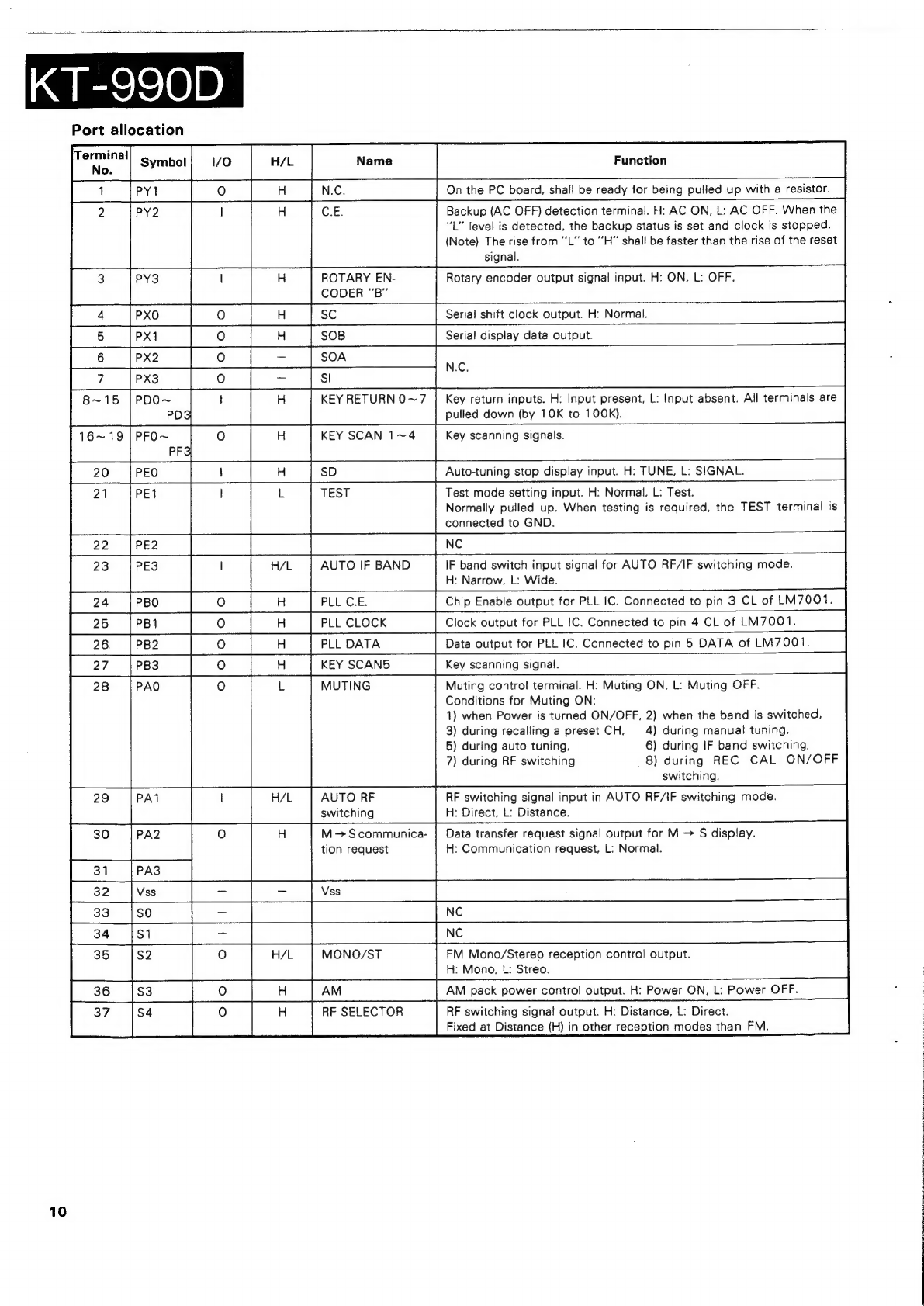
allocation
10
Backup
(AC
OFF)
detection
terminal.
H:
AC
ON,
L:
AC
OFF.
When
the
“L"
level
is
detected,
the
backup
status
is
set
and
clock
is
stopped.
(Note)
The
rise
from
“’L”
to
’H”
shall
be
faster
than
the
rise
of
the
reset
signal.
PY3
H
ROTARY
EN-
Rotary
encoder
output
signal
input.
H:
ON,
L:
OFF.
CODER
“B”
Serial
shift
clock
output.
H:
Normal
so
Serial
display
data
output
so
|
N.C.
H
~
4
8~15
|PDO~
'
KEY
RETURN
O~7
|
Key
return
inputs.
H:
Input
present,
L:
Input
absent.
All
terminals
are
PDS
pulled
down
(by
10K
to
100K).
16~19
|
PFO~
0
KEY
SCAN
1~
Key
scanning
signals.
PF3
H
|
20
[peo
|
1
|
H
SD
Auto-tuning
stop
display
input.
H:
TUNE,
L:
SIGNAL.
21
PE1
|
TEST
Test
mode
setting
input.
H:
Normal,
L:
Test.
Normally
pulled
up.
When
testing
is
required,
the
TEST
terminal
is
connected
to
GND.
Fe
L
H/L
AUTO
IF
BAND
IF
band
switch
input
signal
for
AUTO
RF/IF
switching
mode.
H:
Narrow,
L:
Wide.
Chip
Enable
output
for
PLL
IC.
Connected
to
pin
3
CL
of
LM7001.
[25
[per
[0
|W
PLL
GLOGR
|
tock
output
for
PLL
IG.
Connected
wo
pin
4
CL
of
LM7007.
[26
[pez
[0
[4
PLL ATA
|
ate
output
for
PLL
IC,
Comecied
to
pin
DATA
of
LM7O0T.
28
=
i
nN
Ley)
me)
m
w
|
PA
Muting
control
terminal.
H:
Muting
ON,
L:
Muting
OFF.
Conditions
for
Muting
ON:
1)
when
Power
is
turned
ON/OFF,
2)
when
the
band
is
switched,
3)
during
recalling
a
preset
CH,
4)
during
manual
tuning,
5)
during
auto
tuning,
6)
during
IF
band
switching,
7)
during
RF
switching
8)
during
REC
CAL
ON/OFF
0
1
2
switching.
29
PA
H/L
AUTO
RF RF
switching
signal
input
in
AUTO
RF/IF
switching
mode.
switching
H:
Direct,
L:
Distance.
PA
H
M-—>Scommunica-
|
Data
transfer
request
signal
output
for
M
>
S
display.
tion
request
H:
Communication
request,
L:
Normal.
wo
°
PA3
Vss
Ee
N}o
Freee,
le
Ne
fee
IN
ey
eg
w
9)
—
w
1
Ww
wn Oo
H
MONO/ST
FM
Mono/Stereo
reception
control
output
H:
Mono,
L:
Streo
Vss
AM
pack
power
control
output.
H:
Power
ON,
L:
Power
OFF
RF
SELECTOR
RF
switching
signa!
output.
H:
Distance,
L:
Direct.
Fixed
at
Distance
(H)
in
other
reception
modes
than
FM.
w
a
n
i)
ZL
H
H
°2)
”
w
Wl!
w
N
wn
&
:
|

FM
IF
BAND
REC
CAL
H
R/L
AUTO
STOP
SENS.
LEVEL
IF
band
switching
signa!
output.
H:
Wide,
L:
Narrow.
Fixed
at
Wide
in
other
reception
modes
than
FM.
REC
CAL
reference
signal
transmission
request
signal
output.
H:
REC
CAL
reference
signal
transmission
request,
L:
Normal.
Auto
tuning
stop
sensitivity
switching
signal
output.
H:
High,
L:
Low.
Control
signal
output
of
pin
6
BLK
of
FL
driver
IC
(LC7570).
H:
FL
display
ON,
L:
FL
display
OFF.
N.C.
Only
pin
56
shall
be
set
ready
for
being
pulled
up.
a
FL
-B
power
supply
connection.
ENG
a
H
ROTARY
ENCOD-
|
Rotary
encoder
output
signal
input.
H:
ON,
L:
OFF.
ER
“A”
7
Clock
oscillation
terminals.
X‘tal:
4.194304
MHz.
-,
CL2
Reset
signal
input.
H:
Normal,
L:
Reset.
N.C.
On
the
PC
board,
shall
be
set
ready
for
being
pulled
up.
Preset
channel
memory
@
When
the
MEMORY
key
is
held
depressed
for
more
than
0.2
second
then
the
key
is
released,
preset
channel
display
“—"’
blinks
for
about
5
seconds.
In
this
period,
select
A/B
and
press
a
numeric
key
(1
to
0);
the
preset
channel
memory
is
stored
and
the
stored
channel
is
displayed.
@
When
the
MEMORY
key
is
pressed
again
while
“—"’
is
blinking,
the
display
remains
the
same,
but the
unit
gets
ready
for
another
preset
channel
memory
for
another
5
seconds.
{f
nothing
is
does
after
the
key
has
been
pressed,
the
preset
channel
memory
becomes
impossi-
ble
in
about
5
seconds;
the
preset
channel
display
returns
to
the
last
channel
display,
and
the
MEMORY
indicator
goes
off.
@
When
an
operation
which
is
accompanied
by
muting
is
activated
while
““—"
is
blinking,
the
preset
channel
memory
mode
is
canceled
immediately.
This
occurs
when
one
of
the
RF,
IF,
AUTO
TUNING
SYSTEM,
REC
CAL,
FM
and
AM
keys
is
pressed
or
when
the
rotary
encoder
is
rotated.
However,
if
the
blinking
of
‘“—"
was
started
during
the
AUTO
TUNING
SYSTEM
operation,
the
preset
channel
memory
mode
is
not
canceled
even
when
the
AUTO
TUNING
SYSTEM
key
is
pressed.
@
The
MEMORY
key
is
not
accepted
while
the
muting
timer
is
activated.
@
The
MEMORY
indicator
lights
while
the
key
is
pressed.
When
the
key
is
held
depressed
for
more
than
0.2
second,
the
indicator
continues
to
light
even
after
the
key
has
been
released
and,
at
this
time,
‘“—”
on
the
preset
channel!
display
starts
blinking.
+B
terminal
(5V).
Programming
feature
@
Last
Ch
->
Last
Ch
band
is
ChO
of
A>
ChO
of
a
B:
ChO
of
B-
ChO
of
‘a
REC
CAL
@
During
REC
CAL
operation,
keys
other
than
the
REC
CAL
key
are
not
accepted.
@
The
REC
CAL
operation
is
canceled
by
turning
power
OFF
(when
the
microprocessor
is
reset).
@
The
preset
channel
memory
mode
is
canceled
when
the
REC
CAL
key
is
pressed.
@
When
the
REC
CAL
key
is
pressed
during
frequency
scanning
in
the
Auto
Tuning
mode,
the
frequency
scanning
pauses
temporarily.
The
frequency
scanning
resumes
when
the
REC
CAL
mode
is
canceled
by
pressing
the
REC
CAL
key
again.
@
When
the
REC
CAL
key
is
pressed
during
the
AUTO
TUNING
SYSTEM
operation,
the
AUTO
TUNING
SYS-
TEM
operation
will
be
carried
out
until
the
end.
11
i
|
|
|

KT-990D
12
Keys
valid
only
with
FM
band:
AUTO
TUNING
SYSTEM,
RF,
IF
Display
and
muting
OFF
timing
at
power
ON
(Resetting)
QO
0O5sec
1
sec
3
sec
$$
4
+
+H
up
pin2
PLL
da-
Dispiay
MOTE
CH”
H”
ta
and
ON
OFF
detected
display
data
trans-
ferred
Countermeasure
against
overrun
@
Turn
power
ON
with
the
FM,
RF
and
REC
CAL
keys
held
depressed
simultaneously.
The
microprocessor
will
be
initialized
and
data
including
backup
data
is
cleared.
Other
@
Band
preset
scanning
is
possible
in
Test
mode;
when
the
key
for
the
same
band
is
pressed
successively,
the
preset
memory
channels
for
the
band
are
received
in
sequence.
Initial
setup
condition
Band:
FM
Frequency:
87.50MHz
Tuning
mode:
Auto
RF:
Distance
IF:
Wide
Channel
mode:
A
ST/MONO:
Stereo
Preset
channel:
ay
a)
Bea
SENS
LEVEL:
‘’H”
(all
types).
REC
CAL:
OFF
PROGRAM:
OFF
AUTO
TUNING
SYSTEM:
OFF
Preset
channel
memory:
FM
87.50
MHz
for
all
of
CH1
to
CHO.
AM
initial
setup
condition
Frequency:
530
(631
kHz
E-TYPE)
kHz
RF:
Direct.
However,
all
indicators
including
RF
SEL
are
OFF.
IF:
Wide.
However,
all
indicators
including
IF
BAND
are
OFF.
Channel
mode:
A
ST/MONO:
Mono
regardless
of
tuning
mode
Preset
channel:
4%
Meat
SENS
LEVEL:
“’H”
(all
types).
REC
CAL,
PROGRAM,
AUTO
TUNING
SYSTEM:
OFF

Output
Port
Logic
in
Different
Modes
At
initial
resetting
(when
backup
is
NG)
(FM
Mode)
AUTO
MANUAL
cx
[ép)
ag
as
oe
a
>
loam
430
YAMOd
WV
11
NO
¥3M0Od
WV
:H
Auto
tuning
system
(ATS)
The
ATS
operation
mode
can
be
turned
ON/OFF
only
during
FM
band
reception.
When
the
RF
or
IF
key
is
pressed
during
FM
band
reception,
the
ATS
mode
is
canceled
immediately.
If
the
ATS
operation
has
been
activated,
it
is
also
aborted
at
this
time.
As
the
final
ATS
operation
mode
is
stored
in
memory,
the
ATS
operation
is
started
if
the
final
mode
was
the
ATS
mode
when
the
microprocessor
is
reset,
power
is
turned
ON,
or
when
any
of
the
FM
band
key,
numeric
keys
or
A/B
key
is
pressed
during
receiving
a
band
other
than
FM.
When
the
rotary
encoder
is
rotated
in
the
ATS
mode
or
when
the
ATS
key
is
pressed
during
tuning
(frequency
scanning)
operation,
RF
is
set
to
the
Distance
and
IF
to
Narrow.
However,
if
SD
(microprocessor
pin
20)
“H”
is
not
detected
as
the
result
of
frequency
scanning,
the
RF
and
IF
mode
will
not
change
even
after
the
end
of
frequency
scanning.
Even
when
the
reception
status
changes
after
the
ATS
operation
has
ended,
the
ATS
operation
will
not
resume.
LOSYHIG
*7
JONVISIG
:H
Fo
Lap
5
Crea
nw
zs
Zz
ae
»O
m™>
Z2Zz
am
=z
nn
rot
zs
mm
=
or
i
a
F
=
Oo
c
as
3
a
>"
=
bd
c
3
3.
a
i]
cas
®
=
©
a
Test
Frequencies
that
are
stored
in
memory
cha
nnels
in
test
mode
@
Band
preset
scanning
is
possible
only
in
Test
mode.
Note)
The
Test
mode
is
entered
by
turning
power
FM
rEM
87.5MHz|
FM
87.5MHz,
ON
with
the
A-2
89.1MHz|
89.1
MHz
TEST
terminal
(GND).
As
the
106.0MHz|
106.0
MHz
band
preset
scanning
is
ac-
tivated
in
Test
mode,
these
frequencies
canbe
received
in
sequence
with
out
press-
ingthe
memory
channel
keys,
87.5MHz
87.5MHz
87.5MHz
87.5MHz
87.5MHz
AM
530
kHz
87.5
MHz
87.5
MHz
87.5
MHz
AM
531
kHz
P
o
butby
just
630
kHz
630
kHz
pressing
one
of
990
kHz|
990
kHz]
—theband
swiches
(FM
1440
kHz
1440
kHz
/AM).
1610
kHz
1602
kHz
FM
87.5MHz|
FM
87.5MHz
B-7
87.5MHz
87.5
MHz
87.5MHz|
87.5
MHz
|
87.5MHz|
87.5
MHz
87.5MHz|
87.5
MHz
13

KT-990D
14
Auto
tuning
system
operation
flowchart
Numeric
key,
A/B
key
or
FM
key
pressed
ON?
Rotory
encoder
rotated?
ATS
mode?
RF
:
DISTANCE
IF
:
NARROW
125ms(Normal)
or
500ms{Band
edge)
POWER
ON
RESRT?
Yes
ATS
mode
3sec
inversion
Yes
32msec
Check
SD
{pin
20).
requency
scanning?
RF
:
DISTANCE
IF
:
NARROW
512msec
RF
:
DIRECT
IF
:
NARROW
Muting
cancel
512msec
RF
:
DISTANCE
RF
:
DIRECT
512msec
?
NARROW
IF
512msec

1C1:
LM7001(X05-3420-1
1)
PLL
frequency
synthesizer
|
iF
2
PI
hase
Detector
|
Block
diagram
syc
Charge
Pump
XIN
XOUT
o
FMIN
o
AMIN
o
4$
54
CE
CL
DATA
Terminal
description
Pin
no|
Pin
name
VO
[Function
4
XOUT
oO
EE
ene
IN
Ss
es
ee
Data
input.
Clock
for
controller
(400
kHz).
Band
data
output.
BO1
can
be
used
as
a
time
base
output
(8
Hz)
Local
oscillator
signal
input.
Power
supply.
VDD2
for
back-up.
Charge
pump
output.
Power
supply.
Data
input
11>
10us
|
Data
input
12>
10us
|
titifti
CL
(PIN@)
DATA
(PIN@}
CE
(PIN@)
INTERNAL
DATA

T-990D
1018:
MC1495L
(X05-3420-11)
MPX
SUB
demodulator
MPX
SUB
Decoder
(IC18:
MC1495L)
The
Direct
Pure
MPX
enables
stereo
decoding
without
causing
beat
interference,
in
theory,
by
linear-multiplying
two
analog
signals
(stereo
composite
signal
and
38
kHzsine
wave
sub
carrier
signal).
This
unit
provides
the
linear
multiplier
with
high
S/N
ratio,
which
is
designed
with
the
new
theory.
so
that
the
high
signal-to-noise
rationof
94
dB
for
the
MPX
unit
itself
and
the
resistance
to
overmodulation
of
400%
(dynamic
range:
106
dB
are
realized
while
the
conventinal
characteristics
are
maintained.
Internal
equivalent
circuit
O
2
Output
O
14
(KXY)
38kHz
8
Oo
X
Input
Y
Input
4
O
12
Composite
50
O11
60
O10
30
O13
v
7
1C22:
M5231TL
(X05-3420-11)
Constant
voltage
power
supply
Block
diagram
INPUT
CIRCUIT
OVERHEAT
=
Cy
PROTECTION
OVER-WAVE
OUTPUT
LIMITER
CIRCUIT
.
REFERENCE
VOLTAGE
GENERATOR
PHASE
CONPENSATION
CIRCUIT
VOLTAGE
ADJUSTMENT
16

1C3,
4:
LC7570(X13-5750-11)
FL
driver
IC
Pin
configuration
(Top
View)
Equivalent
block
diagram

T-990D
18
Explanation
of
terminals
SO~S33,
Va:
Segment
outputs,
pull-down
resistor
com-
mon
terminal.
So
$1
$33
Vev
Vop
BLK
:
Display
OFF
input.
BL
R=
0"
(Vos).....eccscscessssscssesssseeeeesserss
OFF
BLK="1"
(Vo)...
csesesecccssssesecsseserereessees
ON
CL,
DATA,
WR
:
Data
inputs
Voo,
Vss
:
Power
supply
terminals
Data
input
CL
Pin
@
DATA
Pin
@
WR
Pin
@®
Display
Input
at
DO
DO~D33
:
Display
data
DA~DE_
:
Dummy
bit
(don’t
care)
DF
:
S29~$33
switching
Dn="1"
;
Sn="1"
(=Voo)
Dn="0"
»
Sn="0"
(=Vr)
De
"+
D29~D33
>
S29~S33
De
="1"
:
ADI
>
$33
AD2
>
$32
AD3
>
S31
AD4
>
S30
AD5
> S29
a
a
I
°
SIN:
AD
converter
input.
1st
point
lighting
level:
0.1
Voo
(typical)
2nd
point
lighting
level:
0.2
Voo
(typical)
3rd
point
lighting
level:
0.3
Voo
(typical)
4th
point
lighting
level:
0.4
Voo
(typical)
5th
point
lighting
level:
0.5
Voo
(typical)
tl>4
usec
t2>4
«sec
t3
>20
psec

FL1:
FIP12AM15S
(X13-5750-1
1)
Fluorescent
indicator
tube
Grid
division
&
|Cosrancr)
&:
71)
Cosmence
=)
[A
MeMons.)
» .
-PROSISN
"=
eeeser
: :
FM
—
(“aro
]
|
ISN.
|
Canvas:
laa
Ll
ea
ee
Bg
:
:
)
Et
Gt
Ele
8
La
TV
[wide]
|
adh
NARROW
(wor)
|
BAND
|
MAIN
suB
BILINGUAL
REC
CAL
6G
5G
4G
3G62G
1G
Anode
Internal
connection
XA
XA
XS
x2
LA
LA
a5~g5
a3~g3
Z4
x1
[STEREO
|
[Memory
]
PROGRAM
FM
wie
(aiblet--
A
Ef
‘
X3
{AO
]
X5
wide]
esol]
NARROW)
a4~g4/
a2~g2
Z2/
ZI
,
x4
DP.
Z3
ide
XA
XS
X6
Pin
No.
Electrode
Pin
No.
Electrode
i
5G
Porm
P%
Paw
4G
Pory
Pin
No.
50
51
52
53
54
55
Electrode
Pu Pu
Pu
NC
Ps
Pin
No.
71
72
Electrode
Py
Pa
Notes
F:
Filament
G:
Grid
P
:
Anode
NC
:
No
Connection

20
INPUT
OUTPUT
TUNER
ALIGNMENT
ITEM
SETTINGS
SETTINGS
SETTINGS
POINTS
ALIGN
FOR
FIG.
FM
SECTION
Unless
otherwise
specified,
the
individual
switches
should
be
set
as
following:
SELECTOR:FM
IF
BAND:
WIDE
RF
SELECTOR:DISTANCE
TUNING
MODE:AUTO
REC
CAL:OFF
Connect
a
DC
(A)
98.
OMHz
Connect
a
DC
L
DISCRIMINATOR
0
dev
voltmeter
between
98.
OMHz
(X86-)
0.000Vt10a¥
(b)
100dBuCANT
input)
P5(AFC)and
TP6CVREF).
Connect
a
DC
BAND
EDGE
voltmeter
between
TUNING
MODE:
(9)
2
BAND
EDGE
voltmeter
between
(2)
TP38(VT)
and
TP4(GND).
9
(A)
Connect
Li2
98.
OMHz
(X86-)
0.000V+20aV
3
98.
OMHz
(X05-)
PROGRAM:
OFF
TUNING
MODE:
ANU
108.
OMHZ
TP3CVT)
and
TP4(GND).|
MANU
87.
5MHz
Repeat
alignments
1
and
2
several
times.
98.
OMHz
a
DC
voltmeter
PLL
DETECTOR
0
dev
between
TP7(¥CC/2)
100dBuCANT
input)
and
TP8(DET).
(A)
Connect
MPX
98.
OMHz
a
frequency
counter
yco
0
dev
between
TP19(GND)
100dBuCANT
input)
and
TP20(VCO).
(A)
1kHz,+75kHz
dev
%
Repeat
the
sequence
from
L1-L4—-+L7--L10—L1------
a
few
times.
(A)
7
IFT(L)
98.
OMHz
(BD
98.
OMHz
1kHz,#75kHz
dev
(A)
IFT(2)
98.
OMHz
(B)
98.
OMHz
1kHz,+75kHz
dev
(A)
98.
OWH2
98.
OMHz
(B)
98.
OMHz
19,
000kH2+10Hz
Maximum
amplitude
and
symmetry
of
the
oscilloscope
display.
Maximum
amplitude
i:
98.
OMHz
=<
:
od
and
symmetry
of
the
oscilloscope
display.
Maximum
amplitude
and
symmetry
of
the
oscilloscope
display.
Position
where
the
STEREO
indicator
lights
when
the
control
is
rotated
gradually
clockwise
from
the
most.
rant
=o
or
naw
1
wv
D
xo
co
oe
1
Vv
AUTO-STOP
SENSITIVITY
SELECTOR:
MAIN
ikH2,275kHz
dev
12dBuCANT
input)
«€)
98.
OMHz
SELECTOR:
MONO
1kHz,+75kHz
dev
*
80dBuCANT
input)
(C)
98.
OMHz
SELECTOR:
MONO
ikHz,t75kHz
dev
*
80dBuCANT
input)
()
DISTORTION
(1)
DET
Minimum
distortion.
DISTORTION(2)
MONO
(B)
98.
OMHz
Minimum
distortion.
98.
OMRz
DISTORTION(3)
SELECTOR:
MONO
(B)
98.
OMHz
VRE
Mininua
distortion.
MONO
1kHz,t75kHz
dev
*
(X86-)
80dBuCANT
input)
Adjust
10,
11
and
12
alternately
a
few
times
to
minimize
the
MONO
distortion.
*
E&
T
types:
1kHz,
t46kHz
dev.
Cc)
98.
OMHz
SELECTOR:
SUB
1kHz,+68.25kHz
dev
Pilot:16.75kHz
dev
80dBuCANT
input)
(Cc)
98.
OMHz
SELECTOR:
SUB
1kHz,
+68.
25kHz
dev
Pilot:26.75kHz
dev
80dBuCANT
input)
After
the
adjustment
of
14,
adjust
13
again
to
minimize
the
distortion
at
1kHz.
DISTORTION(4)
STEREO
YR7
(B)
98.
OMHz
(X86-)
Mininur
distortion.
DISTORTION(5)
STEREO
(B)
98,
OMHz
(X05-)
Miniaua
distortion.
c
oo os
Other manuals for KT-990D
1
Table of contents
Other Kenwood Synthesizer manuals