manuals.online logo
Brands
  1. Home
  2. •
  3. Brands
  4. •
  5. Lectrosonics
  6. •
  7. Microphone System
  8. •
  9. Lectrosonics HH Manual

Lectrosonics HH Manual

Other manuals for HH

2

This manual suits for next models

3

Other Lectrosonics Microphone System manuals

Lectrosonics M175DC User manual

Lectrosonics

Lectrosonics M175DC User manual

Lectrosonics SMWB series User manual

Lectrosonics

Lectrosonics SMWB series User manual

Lectrosonics UDR700 User manual

Lectrosonics

Lectrosonics UDR700 User manual

Lectrosonics UMCWB User manual

Lectrosonics

Lectrosonics UMCWB User manual

Lectrosonics M2T User manual

Lectrosonics

Lectrosonics M2T User manual

Lectrosonics DHu User manual

Lectrosonics

Lectrosonics DHu User manual

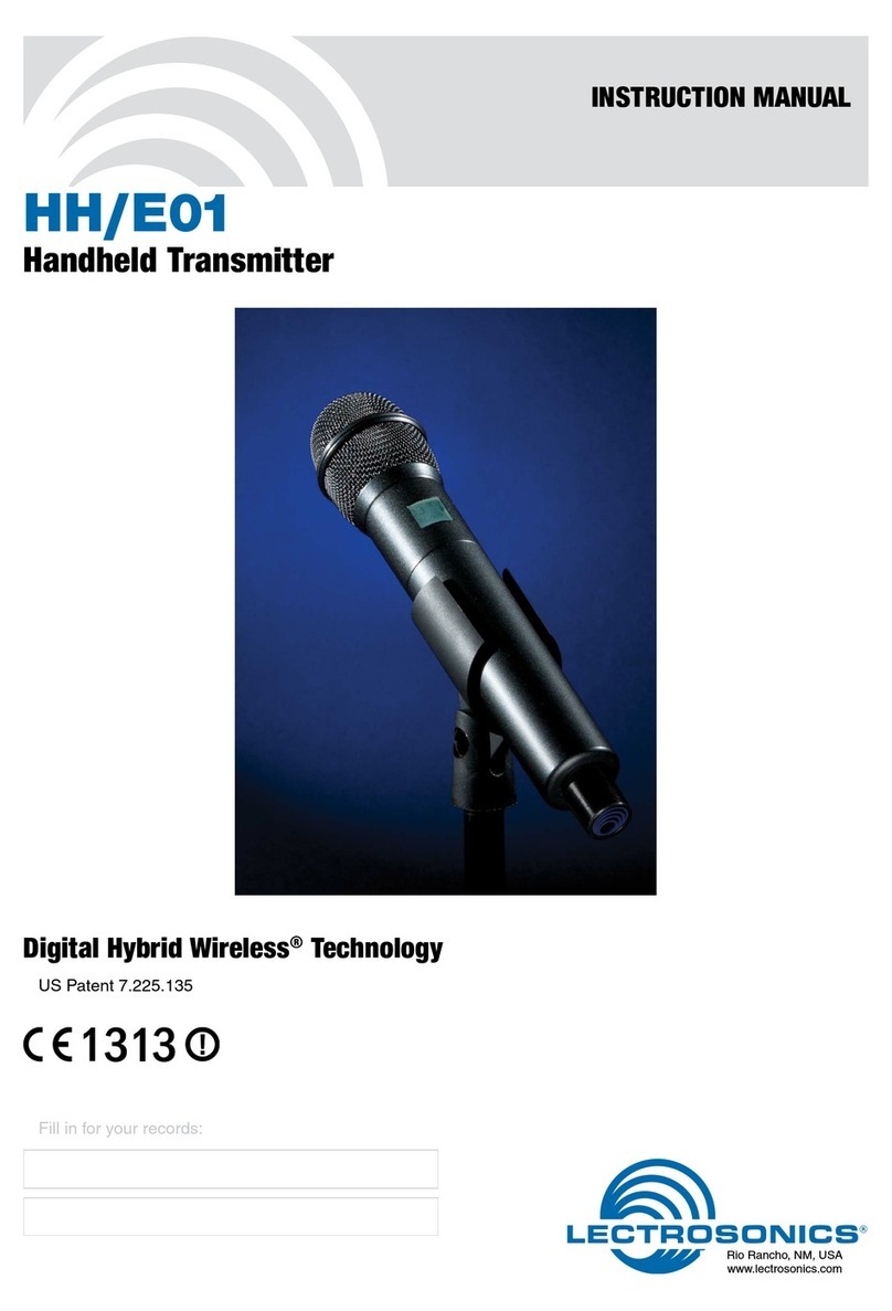
Lectrosonics HH/E01 User manual

Lectrosonics

Lectrosonics HH/E01 User manual

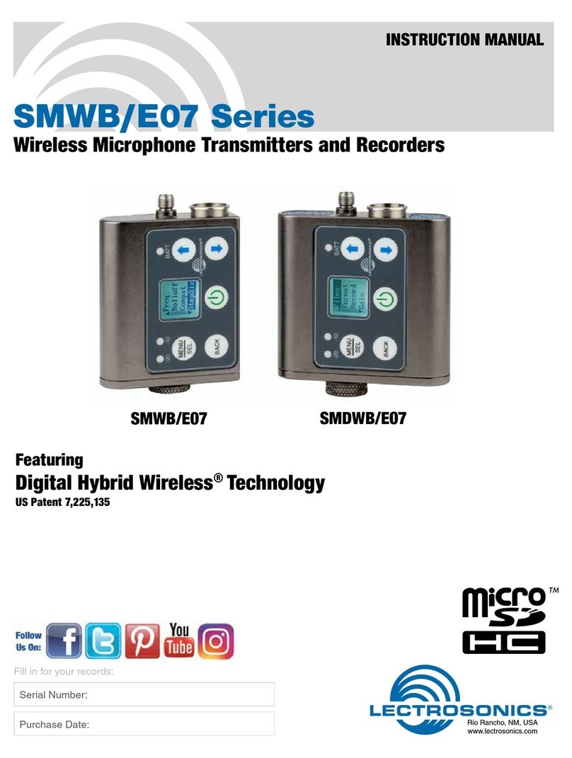
Lectrosonics SMWB/E07 Series User manual

Lectrosonics

Lectrosonics SMWB/E07 Series User manual

Lectrosonics PRO 4 CHANNEL User manual

Lectrosonics

Lectrosonics PRO 4 CHANNEL User manual

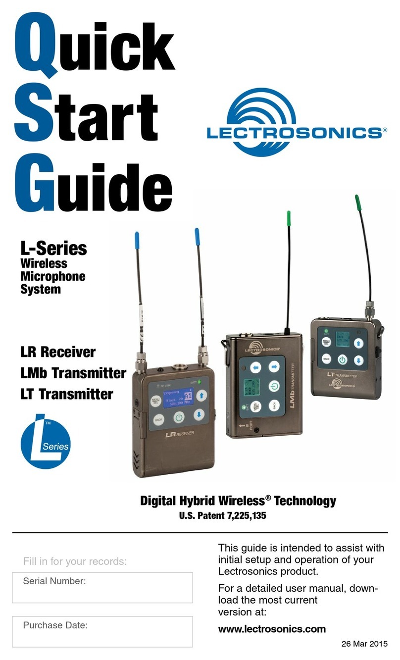
Lectrosonics L series User manual

Lectrosonics

Lectrosonics L series User manual

Popular Microphone System manuals by other brands

INIM SAGITTARIUS VW2W instructions

INIM

INIM SAGITTARIUS VW2W instructions

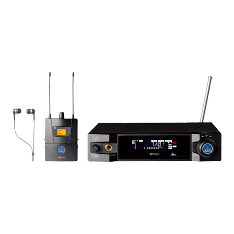
AKG IVM 4500 User instructions

AKG

AKG IVM 4500 User instructions

Earthworks Audio PM40 manual

Earthworks Audio

Earthworks Audio PM40 manual

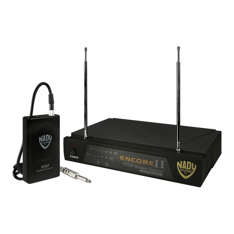
Nady Systems ENCORE 2 owner's manual

Nady Systems

Nady Systems ENCORE 2 owner's manual

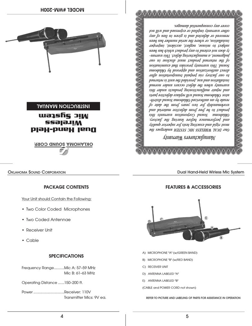
Oklahoma Sound WM-200H instruction manual

Oklahoma Sound

Oklahoma Sound WM-200H instruction manual

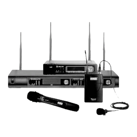
Chiayo SDR-8200 Operation manual

Chiayo

Chiayo SDR-8200 Operation manual

Paso R824 quick start guide

Paso

Paso R824 quick start guide

Naxa NAM-982 instruction manual

Naxa

Naxa NAM-982 instruction manual

Xvive U3 user manual

Xvive

Xvive U3 user manual

Tekon DUOS installation guide

Tekon

Tekon DUOS installation guide

Heyuan Intelligence IOT-G2S-01 user manual

Heyuan Intelligence

Heyuan Intelligence IOT-G2S-01 user manual

Devine WMD-IE user manual

Devine

Devine WMD-IE user manual

LG LF-D7150 owner's manual

LG

LG LF-D7150 owner's manual

LD U305 HBH 2 user manual

LD

LD U305 HBH 2 user manual

Chainway URA8 user manual

Chainway

Chainway URA8 user manual

ORATOR D860TD instruction manual

ORATOR

ORATOR D860TD instruction manual

Sennheiser Evolution Wireless Digital EW-DX EM 2 quick guide

Sennheiser

Sennheiser Evolution Wireless Digital EW-DX EM 2 quick guide

Shure UA844 user guide

Shure

Shure UA844 user guide

manuals.online logo
manuals.online logoBrands
  • About & Mission
  • Contact us
  • Privacy Policy
  • Terms and Conditions

Copyright 2025 Manuals.Online. All Rights Reserved.

Lectrosonics Standard Test & Alignment Procedure
Part number(s): HH Hardware version(s): 17424B (audio) & 17423B (radio) Firmware version(s): 0.93
Part number(s): HHAU Hardware version(s): 17424B (audio) & 17423B (radio) Firmware version(s): ?
Part number(s): HH/E01 Hardware version(s): 17424B (audio) & 17423B (radio) Firmware version(s): ?
Part number(s): HH/E02 Hardware version(s): 17424B (audio) & 17423B (radio) Firmware version(s): ?
Common name: hand held transmitter Author(s): Rodney Wildhagen & Cruz Garcia Test procedure version: 01.00
Date: 04 Oct 2011
Initial setup: Audio Board only
Audio board with PIC18F67J11 µC IC
Step Measurement name& description Measurement result (Typ)
Test Segment 10 of 60
Program µC IC and Current draw Audio board only
CAUTION When reprograming already tested devices, be sure to set device programmer GUI to preserve all settings (block,
limiter settings, etc.). In Microchip MPLAB this is done by selecting Programmer > Settings > Program > Preserve
EEPROM on program > Apply > OK. Failure to do so will result in loss of all assigned variable values such as
frequency block, limiter setting, indicator settings, etc.
Note This need only be performed at the factory the first time the DUT is powered up, when µC IC is replaced, or when a
firmware update is desired and confirmed to be appropriate.
Apply +3.0VDC, 300mA current limit in at battery contact J8 (J9 is circuit common)
Note In order to program DUT, JU1 must be jumpered or the power button must be pressed during the entire
programming process. Remove JU1 jumper after programming.
Program µC IC with programming cable connected at J6 (ICSP port)
Remove ICSP cable
Measure current draw 50 to 500 mA (117)
Note The goal here is only to ensure the audio board powers up and is not burning up with fever
Remove DC voltage from Battery contacts and apply firmware version label to audio board
Test Segment 20 of 60
NOTE: This segment may be performed using one audio board to test multiple radio boards
Initial setup:
Known good, pre-tested audio board with PIC18F67J11
µC IC running firmware version appropriate & current for
part number connected to an untested radio board
Test panel key pad or appropriate test rig connected to
audio board J2
Apply +3.0VDC, 300mA current limit in at battery contact
J8 (J9 is circuit common).
All voltage measurements referenced to circuit common
All demodulated carrier and carrier deviation
measurements taken with a Hewlett Packard 8901B
modulation analyzer with no 8901B filters selected. Use of
other instruments may yield different results particularly
measurements pertaining to noise and phase and
measurements where noise is a significant factor
All audio stimulus signals applied to audio input rig
defined at foot of this document
All audio stimulus signals are single ended.
Carrier power for various part numbers are as follows:
HH=100mW, HHAU & HH/E01=50mW and HH/E02
All audio measurements taken with a ≤10 Hz HPF and
80KHz LPF (use filter on audio signal analyzer, no
modulation analyzer unless otherwise specified).
This font indicates use of the
A
lternate Method to manual testing. The
Alternate Method uses the LectroLink
apparatus and either the LecNet2
Command Terminal Utility or the
O:\ATE\MTE\HH\
H
H_LectroLink_Control.exe
program. Test steps bearing the same
number indicates alternate method(s).
Step Measurement name & description Measurement result (Typ)
Power Up sequence and current draw
Prerequisite(s): FPGA IC programmed
Hold test power button on test panel key pad for 3 seconds until DUT powers up
Observe behavior of test key pad LED -10 LED turns on red, then -20 LED
turns on red then both off.
both LED's flash red once then
green once
Observe behavior of test audio board LCD "HH"
"Vx.xx"
"block XX"
"Hybrid"
?
?
?
?
frequency "Main" screen
Note a flashing antenna icon inside a ׎indicates the PLL is not locked
Measure current draw 50 to 500 mA (145)
Note The goal here is only to ensure the DUT powers up and is not burning up with fever
Audio board frequency block assignment
Prerequisite(s): FPGA IC programmed
Note: This part has to be performed only on the first DUT to setup Test Audio Board for the Block.
Momentarily connect audio board TP5 to TP22 (enter Set-up mode)
Note Entering Set-up mode is not necessary if the Alternate Method is exercised.
Using the test key pad navigate to the "Block" screen.
Press UP or DWN button on the test panel key pad to change unit to desired Block
block= (set freq block 470,19-33, 944 standard 400-999 extended)
Turn DUT Off then back On and check to see if the Block set.
VCO adjustment & VCO start-up test
Prerequisite(s): FPGA IC programmed
Using the test key pad navigate to the "Freq." screen
Press MENU/SEL and UP button simultaneously to change frequency to highest frequency. (pressing MUNU/SEL
and UP simultaneously will step the frequency up in increments of 16 only pressing the UP or DOWN buttons will
only increment by 1)
channel=XX set channel (0(00) to 1020 (ff) in normal
tuning mode, 80 is 512)
Adjust radio board C1 for 2.5 VDC at radio board TP1 (VCO_CONT) +2.45 to +2.55 VDC (+2.5)
No DC power in at battery contacts
Wait until transmitter completely powers down (approx. 4 sec)
Apply +3.0VDC, 500mA current limit in at battery contact J8 (J9 is circuit common)
Hold Power button for 3 seconds (make sure unit come on).
Measure carrier signal power to be sure the VCO starts on power up at selected
carrier frequency ≥+10 dBm
Using the test key pad navigate to the "Freq." screen
Press MENU/SEL and UP button simultaneously to change frequency to lowest frequency. (pressing MUNU/SEL
and UP simultaneously will step the frequency up in increments of 16 only pressing the UP or DOWN buttons will
only increment by 1)
channel=XX set channel (0(00) to 1020 (ff) in normal
tuning mode, 80 is 512)
Measure DC voltage at radio board TP1 (VCO_CONT) +0.6 to +1.2 VDC
No DC power in at battery contacts
Wait until transmitter completely powers down (approx. 4 sec)
Apply +3.0VDC, 500mA current limit in at battery contact J8 (J9 is circuit common)
Hold Power button for 3 seconds (make sure unit come on).
Measure carrier signal power to be sure the VCO starts on power up at selected
carrier frequency ≥+10 dBm
Carrier signal power adjustments & spectral purity measurements
Prerequisite(s): FPGA IC programmed
Momentarily connect audio board TP22 to J5 pin 4 (enter Set-up mode)
Note Entering Set-up mode is not necessary if the Alternate Method is exercised.
Note Power Measurement are made with the output of the DUT connected directly to the power measuring device to
ensure measurement is as accurate as posable .
Using the test key pad navigate to the "PwrCal" screen
Note
This sets the DUT to "L" (50mW) carrier power at the Mid carrier frequency, from here pressing the UP or DWN
buttons adjusts carrier power. Pressing MENU/SEL button once will move to the Low carrier freq. UP and DWN
buttons adjusts carrier power. Press MENU/SEL again moves to the highest frequency, UP and DWN buttons
adjusts carrier power. Pressing MENU/SEL once more moves to "H" (100mW) at the Mid freq and the pattern
continues to set power for 100mW..
Measure current draw
Repeat this process until all 6 carrier signal power points have been adjusted and double checked after the last
adjustment has been made
Current draw tolerances
for test procedure segment
#20
50mW 100mW
160 to 196
mA (178)
191 to 233
mA (212)
Carrier signal power tolerances for test
procedure segment #20
50mW 100mW
HH +15 to +19dBm +18 to
+22dBm
HHAU 16 to 17.5dBm
HH/E01 +14.8 to -
18.8dBm
HHB/E02 9.5 to 11.1dBm
powercal(p,s)=
set transmitter power calibration parameter, "p" selects
the power level must be 50 or 100, "s" specifies the
carrier frequency within the block and must be 0 for
block bottom, 1 for block middle, or 2 for block top
Note
Carrier power may alternatively be adjusted by first querying the powercal
value "powercal(50,0)?" and subsequently incrementing or decrementing carrier
power using "p=+2" syntax.
Test Segment 30 of 60
NOTE: This segment may be performed using one known good pre-tested audio board to test multiple radio boards
Spectral purity measurements and RF Mute function
Prerequisite(s): FPGA IC programmed
Connect RF Board J3(J4 common) DUT output to a splitter that feeds to the SpecAn, Frequency Counter high
frequency input and the ModAn.
Momentarily connect audio board TP22 to J5 pin 4 (enter Set-up mode)
Note Entering Set-up mode is not necessary if the Alternate Method is exercised.
Apply +3.0VDC, 500mA current limit in at battery contact J8 (J9 is circuit common)
Using the test key pad navigate to the "PwrCal" screen
Step thru all 6 PwrCal measurement while checking for spurs using both prescribed setting in the next steps. This
will result in 12 different spur measurements.
Measure spurs 5 to 1495MHz RBW=30kHz, VBW=10kHz ≤-65 dBc
Note Neither the 2nd nor the 3rd harmonic should be considered as a spur
Measure spurs carrier freq +/- 20MHz RBW=30kHz, VBW=10kHz ≤-65 dBc
Using the test key pad navigate to the "Standby" menu and press the MENU/SEL to activate RF Mute
Measure RF carrier output at radio board J3 ≤-60 dBc
Press MENU/SEL button again to get to the "Xmit" menu, Pressing MENU/SEL again take unit out of "Standby"
Measure carrier signal power to at radio board J3 ≥+5 dBm
Using the test key pad navigate back to the frequency "Main" screen
Modulation level and distortion adjust
Prerequisite(s): FPGA IC programmed
DUT at middle carrier frequency
channel=XX set channel (0(00) to 1020 (ff) in normal
tuning mode, 80 is 512)
NOTE BL944 specimens are permitted to exhibit 150% of otherwise allowable distortion. Some products have required this
additional margin, others have not. At the time of this writing it is unknown how this product will shake out.
Momentarily connect audio board TP22 to J5 pin 4 (enter Set-up mode)
Note Entering Set-up mode is not necessary if the Alternate Method is exercised.
pilotbp=1
Using the test key pad navigate to the "DevOff" screen (Mid carrier freq is highlighted)
tone=1 (sets DSP 1kHz test tone mode ON)
Adjust radio board R26 for minimum modulation distortion at demodulated
carrier
≤1.0 % THD+N (0.7)
Adjust radio board R47 for 100kHz peak deviation at radio board J3 99 to 101 kHz (100)
Press MENU/SEL button on the test panel key pad (Lowest carrier freq is highlighted)
channel=XX set channel (0(00) to 1020 (ff) in normal
tuning mode, 80 is 512)
Measure distortion at demodulated carrier, fine adjusting radio board R26 if
required ≤1.2 % THD+N (0.7)
Press UP or DWN button on the test panel key pad for 100 kHz peak carrier
deviation at radio board J3 99 to 101 kHz (100)
devoff(0)? (Get deviation offset setting for the Low
channel) (+10 to -10). devoff(0)=x (set deviation
offset for 100KHz)(1KHz steps).
99 to 101 kHz (100)
Press MENU/SEL button on the test panel key pad (Highest carrier freq is highlighted)
channel=XX set channel (0(00) to 1020 (ff) in normal
tuning mode, 80 is 512)
Measure distortion at demodulated carrier, fine adjusting radio board R26 if
required
≤1.2 % THD+N (0.7)
Press UP or DWN button on the test panel key pad for 100 kHz peak carrier
deviation at radio board J3
99 to 101 kHz (100)
devoff(1)? (Get deviation offset setting for the high
channel) (+10 to -10). devoff(1)=x (set deviation
offset for 100KHz)(1KHz steps).
99 to 101 kHz (100)
Repeat this step until no further adjustment is necessary
Press BACK button on the test panel key pad to get back to the frequency "Main" screen
tone=0 (turns off DSP 1kHz test tone)
Test Segment 40 of 60
Install VCO shield cover
No DC power in at battery contacts
Disconnect radio board from audio board
Install VCO shield assembly Part number ?
Bend tabs at 45 degrees and Solder around the VCO shield
Allow to cool for a minimum of 10 minutes
Test Segment 50 of 60
NOTE: This segment must be performed using the audio/radio board pairs that will remain paired up
Setup:
Audio board with PIC18LF6J11 µC IC running firmware
version appropriate & current for part number connected
to an untested radio board, these boards will live together
til death do they part.
Test panel key pad connected to audio board J3
Apply +3.0VDC, 500mA current limit in at battery contact
J8 (J9 is circuit common)
All voltage measurements referenced to circuit common
All demodulated carrier and carrier deviation
measurements taken with a Hewlett Packard 8901B
modulation analyzer with no 8901B filters selected. Use o
f
other instruments may yield different results particularly
measurements pertaining to noise and phase and
measurements where noise is a significant factor
All audio stimulus signals applied to audio input rig
All audio stimulus signals are single ended.
Carrier power for the various part numbers are as follows:
HM=100mW, HMAU & HM/E01=50mW and HM/E02
All audio measurements taken with a ≤10Hz HPF and
80KHz LPF (use filter on audio signal analyzer, not
modulation analyzer unless otherwise specified).
This font indicates use of the
A
lternate Method to manual testing. The
alternate Method uses the LectroLink
apparatus and either the LecNet2
Command Terminal Utility or the
O:\ATE\MTE\HM\
H
M_LectroLink_Control.exe
program. Test steps bearing the same
number indicate alternate method(s).
Connect Power Meter Head to RF Board J3(MT4 is circuit
defined at foot of this document, see below common).
Power Up sequence and current draw
Prerequisite(s): FPGA IC programmed
Hold power button on test panel key pad for 3 seconds.
Observe behavior of test key pad LED -10 LED turns on red, then -20 LED
turns on red then both off.
both LED's flash red once then
green once
Observe behavior of test key pad LCD "000000"
"HH"
"Vx.xx"
"Hybrid"
?
?
?
?
frequency "Main" screen
a flashing antenna icon inside a ׎indicates the PLL is not locked
Measure current draw 50 to 500 mA (170)
Note The goal here is only to ensure the audio board powers up and is not burning up with fever
20.20 Control Panel switch test
Prerequisite(s): FPGA IC programmed
Apply +3.0VDC, 500mA current limit in at battery contact J8 (J9 is circuit common)
LCD display and push button key pad installed
Observe LCD display and
verify the frequency "Main"
screen is displayed
buttons?
realtime button status bitmap
(menu/sel=128, back=64, up=1,
down=2, "4=4", "3=8", "2=16",
"1=32", no button=0)
ok 0 (no
tolerance) (0)
Press and release control
board Menu/Sel button
Observe change in menu on
LCD to the Menu screen
press and hold
Menu/Sel
buttons?
realtime button status bitmap
(menu/sel=128, back=64, up=1,
down=2, "4=4", "3=8", "2=16",
"1=32", no button=0
ok 1 (no
tolerance) (1)
Release Menu/Sel
button
Press and hold control board
Down button
Observe change in highlighted
menu on LCD
buttons?
realtime button status bitmap
(menu/sel=128, back=64, up=1,
down=2, "4=4", "3=8", "2=16",
"1=32", no button=0)
ok 16 (no
tolerance) (16)
Release Down button
Press and hold control board
Up button
Observe change in highlighted
menu on LCD
buttons?
realtime button status bitmap
(menu/sel=128, back=64, up=1,
down=2, "4=4", "3=8", "2=16",
ok 32 (no
tolerance) (32)