- 10 -
Copyright 2007 LG Electronics. Inc. All right reserved.
Only for training and service purposes
LGE Internal Use Only
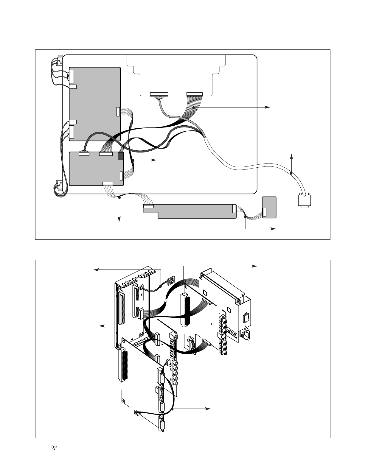
DESCRIPTION OF BLOCK DIAGRAM
1. Input Selection Circuit
This block is composed of 74VHCT126A(U10,U11)
and peripheral devices.
There are two inputs, Analog and Digital H/V Sync.
74VHCT126A(U10,U11) chooses one input and
outputs selected input through sync selection pin (Pin
1,4,13).
2. A/D Converter
This block is composed of AD9888 (U12) and
peripheral devices. AD9888(U12) includes A/D
converter, Pre-amp, and PLL.
The basic RGB signal (0.7Vp-p) is input to R,G,B pin
of AD9888(U12).
Input video signal is amplified, Phase locked , A/D
converted to 8bits digital signal by this IC(U12) And
send the Digital video signal to MX88L285(U62).
U12 makes clock for MX88L285(U201)
3. TMDS Receiver
This Block is composed of SiI161B (U2,U17) and
peripheral devices.
This ICs decodes TMDS Input signal from DVI-I(J1)
and DVI-D Pin (J2) and make 8bit digital signal to
send Digital signal to MX88L285(U201).
4. DDC controller
This block is composed of P89C662F(U43) and
peripheral devices. P89C662F(U43) controls
peripheral devices through IIC line.
Major functions are (1) to control Flash memory
through DDC-SCLA, DDC-SDAA of D-sub And (2) to
store EDID data in the EEPROM (U34,U49,U50)
5. Video Decoder
This block is composed of VPC3230D(U601) and
peripheral devices.
P89C662F(U43) controls this IC through IIC Line.
This IC analyzes input signal of CVBS, Y/C, Y/Pb/Pr
and output analyzed signal (8bit interlace signal) to
De-interlace block.
Analyzed signal has video control signals like
Contrast, Brightness, Sharpness, Color, tint signals
Including Adaptive Comb Filter.
6. DTV Circuit
This block is composed of AD9883(U14) and
peripheral devices. AD9883(U14) includes A/D
converter, Pre-amp, and PLL.
Input video signal is amplified, Phase locked , A/D
converted to 8bits digital signal by this IC(U14) And
send the Digital video signal to MX88L285(U201).
U14 makes clock for MX88L285(U201)
7. Audio Decoder
This block is composed of MSP3420G (U3) and
peripheral devices.
P89C662F(U43) controls this IC through IIC Line.
This IC analyzes Audio input signal through A/V Jack
and PC1/2 audio, DVD/DTV audio.
8. De-interlacer
This block is composed of FLI2310(U302) and
peripheral devices.
P89C662F(U43) controls this IC through IIC Line.
And this IC convert 8 Bit Interlace Y/UV signal to De-
interlace signal.
It output converted signal to Format Converter
(MX88L285)U201.
9. Format Converter
This block is composed of MX88L285(U201),
MX29LV004B(U28), EM638325(U26,U27) and
peripheral devices.
P89C662F controls this IC through parallel line.
MX88L285(U201) processes outputs of A/D
Converter and TMDS Receiver, DTV circuit,
De-interlace output and output processed 48 Bit
Digital signal to TMDS Transmitter.
MX88L285(U201) is Format Converter IC that receive
Digital signal and output proper frame signal to LCD
Module(1920 x1200).
10. Panel-Link Circuit
TMDS Transmitter (SIL160, U9) is the IC that
receives output digital signal of MX88L285(U201) and
output to LCD Module.
The signal format is Panel-link.
LCD Module has Panel-link receiver that is same
output of MX88L285(U201).
This is the best for reduction EMI problem and the
number of pin connector.
11. DC/DC Converter block
DC/DC Converters convert the input 18V to proper
1.8V, 2.5V, 3.3V, 5V, 8V for main board.
For shooting heat trouble, we use the DC/DC
converting IC.