LG GoldStream LW1100P User manual

LG GoldStream
WilessLAN PCI Card
Model Name : GoldStream
Model No. : LW1100P
May , 2001
LG Electronics Inc.

LG GoldStream
Table of Contents
1. Introduction …………………………………………………………………………3
2. Circuit Description ………………………………………………………………… 3
3. Specifications …………………………………………………………………………9
3.1 General Specification ………………………………………………… 9
3.2 Electrical Specification ………………………………………………… 9
3.3 Environmental Specification ……………………………………………9
3.4 Mechanical Specification ………………………………………………10
3. Layout …………………………………………………………………………………… 10
3.1 Block Layout ……………………………………………………………… 10
3.2 PCB Profile ………………………………………………………………… 10
4. Block Diagram ……………………………………………………………………… 11
5. Circuit Diagram ……………………………………………………………………… 12
6. Component Layout ………………………………………………………………………… 13
6.1 Top Side (Component Layer) ………………………………………………………… 13
6.2 Bottom Side (Solder Layer) ………………………………………………………… 14
7. Part List ………………………………………………………………………………… 15
8. Photographs …………………………………………………………………………………16
9. Instruction Manual ……………………………………………………………………… 17

LG GoldStream
1. Introduction
This paperdescribes the GoldStream PCI Card circuits, specifications,layouts and partlist etc.
2. Circuit Description
2.1 The Architecture
The radio design is centered on the expected signalcharacteristics of the modulation method. A
Differential Quadrature Phase Shift Keying (DQPSK) modulation encodesthedatainterms of phase
with minimal amplitude variation, improving noise immunity. This is joined with the IEEE 802.11
protocol standard Carrier Sense Multiple Access/CollisionAvoidance (CSMA/CA)andwith theFCC
requirement for 10dBprocessing gain, to allowsignals to be received with approximately 0dB Signal
to Noise Ratio (SNR) for a 10-5Bit Error Rate (BER). The CSMA/CA protocol allows only one user,
perchannel,ata time(i.e., first come, firstserve)making for aquietermedium. The processing gain,
achieved by spreading the signal with a PN code, allows a faint signal to be pulled from the noise
while suppressing non-correlatinginterferers. Fromthe antenna, thereceivedinput is appliedtothe
pre-selectfilterFL1.Thisfilterisatwopoledielectricdesign,rejectinginterferersoutsidethe2.4GHz
ISM band and providing image rejection.
The signal enters the HFA3683 RF/IF Converter, first passing through the integrated LNA section
and then enters the down converter section of the HFA3683. Low-side local oscillator injection is
used to mix down to the single intermediate frequency, 374MHz. The IF receive filter FL3, is a
SurfaceAcousticWave(SAW)device used for channel selection withinthe band. The SAWoutputis
reactively matched to the IF input of the HFA3783Quadrature IF Modulator/Demodulator.Inreceive
mode,theHFA3783provides two limiting amplifiers,aquadrature basebanddemodulator,and two
baseband low pass filters. The two limiting amplifiers or limiters provide most of the receiver gain,
giving the radio it’s sensitivity.
Thebasebandcircuitsamplesthe waveform with7-bit ADCs and thendespreads anddemodulates
the received data.
On the Transmit side, data can either be DBPSK or DQPSK modulatedat1MSPS(MegaSymbols
Per Second), resulting in a baseband quadrature signal with I and Q components.These digital
signals are output to the HFA3783fifthorder Butterworthlowpass filters,whichareusedto provide
shapingof the phase shiftkeyed (PSK) signal.Therequiredtransmit spectral mask, at the antenna,
is -30dBc at the first side-lobe relative to the main lobe.
The signals are thenquadrature modulated up to IF using the same 2xLO used for the quadrature
demodulation. Thesignal thengoes tothe highimpedance inputoftheHFA3683 upconvertingmixer
for conversion to the 2.4GHz -2.5GHz band. The mixer output goes to the pre-amplifier, in the
HFA3683, amplifies the signal andeasing the requirement for HFA3983 RFPA gain.

LG GoldStream
FL2, a two pole dielectric bandpass filter, is used to suppress both transmit LO leakage and the
undesired sideband. The HFA3983 RFPA amplifies the transmit signal to approximately +18dBm.
The transmit sidelobe performance is approximately -30dBc. Allowing for a 3dB loss in the band
select filter FL1, this gives a final output power of +15dBm.
2.2 Transmit Chain Front End Cascade Analysis
The large gain in the Power Amplifier, HFA3983, keeps the signal level small for the whole chain
before it. This helpsconserve supply current and the cost associated with devices that need to
handle large signals.
The output power at the RF filter is shown as 15dBm, with the output of the Power Amplifier at
18dBm. The design has been optimized for the best use of supply current and cost ofthe PA. If the
output power was lower, the supply current and cost of the PA could be saved with smaller and
cheaperdevices. If the output power was higher, the signal will be too close to the P1dB and the
signal willhaveexcessive distortion, causingregrowth of theside lobes. The transmittedsignalmust
suppress side lobes to -30dB to meet the 802.11 spectral mask specification.
Therefore, the output power needs to be controlled very carefully. The run to run variation in gain
andinsertionlossofthe elements in the transmit chain requires either a manual poweradjustmentor
an active power adjustment feedbackcircuit.Inthisdesign,amanual potentiometeris usedto adjust
output power and side lobe performance on each unit during manufacturing. For purposes of this
analysis, the variable attenuator shows 0dB loss and the Modulator outputas -12dBm. This was
done for illustration purposes only, in actuality the Modulator output has a relatively large output
(200mV P-P ) that needs to be significantly attenuated to the level indicated.
2.3 Power Amplifier(HFA3983)
The HFA3983 is fabricated in the fastest SiGe BiCMOS process available, allowing superior RF
performance, normally found only in GaAs ICs. Cost effective functions, normally requiring external
components, are integrated into one IC. The HFA3983 integrates the following functions in one
compact 28 pin EPTSSOP:
Two Stage, 30dB Gain RFPA,
Logarithmic power detect function (15dB Dynamic Range),
CMOS level compatible Power Up/Down function,
Single Supply, 2.7V to 3.6V Operation.
The HFA3983 contains a highly linear RFPA designed to deliver 18dBm and meet an ACPR
specification of-30dBcin the2.4 to2.5GHz ISMband. Theperformance ofthistwo stage RFPA can
be optimized by adjusting the bias current in each stage with a dedicated resistor. No external
positive ornegative power supplies are required to set the biascurrents.Theonchip bias network
provides the optimum bias current temperature compensation when low TCexternal resistors are
used. To get the best performance from the HFA3983, the output stage matching network canbe
tailored using external components.

LG GoldStream
2.4 2.4GHz RF/IF Converter and Synthesizer(HFA3683)
TheHFA3683A isa monolithicSiGe half duplex RF/IFtransceiver designed tooperateinthe2.4GHz
ISM band.The receive chain features a low noise,gain selectable amplifier (LNA) followed by a
down-converter mixer. An up-converter mixer and a high performance preamplifier compose the
transmit chain. The remaining circuitry comprises a high frequency Phase Locked Loop (PLL)
synthesizer witha threewire programmableinterfaceforlocaloscillatorapplications. Areducedfilter
count is realized by multiplexing the receive and transmit IF paths and by sharing a common
differentialmatching network.
2.5 I/Q Modulator/Demodulator and Synthesizer(HFA3783)
The HFA3783 is a highly integrated and fully differential SiGe basebandconverter forhalf duplex
wireless applications. It features all the necessary blocks for quadrature modulation and
demodulation of “I” and “Q” baseband signals.
It has an integrated AGC receive IF amplifier with frequency response to 600MHz. The AGC has
70dBofvoltagegain andbetter than70dBof gain controlrange.The transmitoutput also features
gain control with 70dB of range.
The receive and transmit IF paths can share a common differential matching network to reduce the
filter component countrequired for singleIF half duplex transceivers.A pair of 2nd order antialiasing
filters with an integrated DC offsetcancellation architecture is included in the receive chain for
baseband operation down to DC. In addition, an IF level detector is included in the AGC chain for
threshold comparison.Up and downconversion are performedbydoubly balancedmixersfor “I”and
“Q” IF processing. These converters are driven by a broadband quadrature LO generator with
frequency of operation phase locked by an internal 3 wire interface synthesizer and PLL.
Inthe transmitpath,DCcoupleddualsingleendto differentialbasebandbuffershavebeenaddedto
the design to help interface the device with standard single end ground referenced source equipment.
The differential buffer also applies therequired common modevoltage (VREF) superimposedtothe
desiredsignalinputtoeachoneofthe differentialbaseband inputs. In addition,a set of jumperpins
(TX±, TX±) have also been added to permit direct monitoring of the differential stimulus/ DC
differential offset or application of external baseband signals bypassing the evaluationboardbuffers.
Anoutputdifferentialoffsetnull capability is included and can be adjusted to zero for DC offset or to
generate adjustable differential DC levels for carrier generation (vector modulation).
The 2XLO local oscillator generation is done by an on board 748MHz VCO. The PLL set for a loop
bandwidth of 1kHz at 25?mA. Its output canbe monitored thruan onboard losspad for phase noise
and spurious responses when switching from transmittoreceivemode.Themonitorportcanalsobe
used as an input,taking the padlossin consideration forevaluation,when using external VCO’s or
generators, providing the on board VCO is disabled.
A couple of powersupply regulators have beenadded to improvethetransmitandreceiveswitching

LG GoldStream
characteristics of the HFA3783. DC current transients which occurs when the device is switched
from transmit to receive cause VCO spurs to appear.
2.6 PLL
The HFA3783 includes a classical architecture Phase Lock Loop circuit with a three wire serial
control interface to be usedwith anexternalVCO.Itconsistsofaprogrammable “R”counter used to
divide down the frequency of a very stable referencesignalupto50MHztoaphasecomparator.A
couple of counters (“A” and “B”) with a front end prescaler(“P or P+1”), with dual modulus control,
divides down the frequency of an external VCO signal to the same phase comparator. The
comparatorcontrols acharge pumpcircuitandanexternalloopfilterclosestheloopforVCOcontrol.
The VCO frequency dividing chain works with a dual modulus control as follows: At the beginning of
a count cycle,and if the Acounteris programmed withavaluegreater than zero,the prescaler isset
to a division ratio of(P+1) where P can take programmable values of 16 or 32.
Notice that the prescaler output signal is always fed simultaneously to both A and B counters.Upon
filling counter A, the prescaler division ratio becomesPandtheB counter continuesonits ownwith
A standby. This processis known as “pulse swallowing”. The expression B-A (counts) is the
remainder of counts carried out by the B counter after A is full. Both A and B counters are reset at
the end of the countingcycle whenBfills up.As aresult,the totalcount ordivision ratio used for the
VCO signal is A*(P+1) + (B-A)*P which simplifies to [P*B+A]. (A and B counters are referred as the
“N” counter).
TheCharge Pump(currentsource/sink) has4 programmable current settings. This variation allows
the user to change the reference frequency for different objectives without changing the loop filter
components. The user can program the charge pump sign based on the direction of increase or
decrease of the VCO frequency. The most often used VCO’s in the market have positive KVCO’s
where the VCO frequency increases with an increase in control voltage. In this case, the charge
pump current shall “source” current (to the main capacitor of the loop filter) whentheVCOfrequency
becomes less than the desired frequency of operation.
2.7 Direct Sequence Spread Spectrum Baseband Processor(HFA3861)
The HFA3861B has on-board A/D’s and D/A for analog I and Q inputs and outputs, for which the
HFA3783 IF QMODEM is recommended. Differential phase shift keying modulation schemes
DBPSKand DQPSK,with datascramblingcapability, areavailablealong withComplementary Code
Keying to provide a variety of data rates. Both Receive and Transmit AGC functions with 7-bit AGC
control obtain maximum performance in the analog portions of the transceiver. The HFA3861B is
housed in a thin plastic quad flat package (TQFP) suitable for PCMCIA board applications.
TheHFA3861BtransmitterisdesignedasaDirect Sequence Spread Spectrum Phase Shift Keying
(DSSS PSK) modulator. It can handle data rates of up to 11Mbps(refer to AC and DC specifications).
The various modes of the modulator are Differential BinaryPhaseShiftKeying(DBPSK) for 1Mbps,

LG GoldStream
Differential Quaternary Phase Shift Keying(DQPSK)for2Mbps,andComplementaryCodeKeying
(CCK) for 5.5Mbps and 11Mbps. These implementdata rates as shown in Table 3. The major
functional blocks of the transmitter include a network processor interface, DPSK modulator, high rate
modulator, a data scrambler and a spreader, as shown in Figure 7. CCK is essentially a quadra-
phase form of M-ARY Orthogonal Keying. A descriptionofthatmodulationcan befoundinChapter 5
of: “Telecommunications System Engineering”, by Lindsey and Simon, Prentis Hall publishing.
The preamble is always transmitted as the DBPSKwaveformwhile the headercanbe configured to
be eitherDBPSK,or DQPSK,and datapacketscan beconfigured forDBPSK,DQPSK,orCCK.The
preamble is used by the receiver to achieve initial PN synchronization while the header includes the
necessary data fields of the communications protocol to establish the physical layer link. The
transmitter generates the synchronization preamble and header and knows when to make the
DBPSK to DQPSK or CCK switchover, as required.
-Header/Packet Description
The HFA3861B is designed to handle packetized Direct Sequence Spread Spectrum (DSSS) data
transmissions.The HFA3861B generates its own preamble and header information.Itusestwopacket
preambleandheaderconfigurations. The firstis backwards compatiblewith the existing IEEE 802.11-
1997 1 and 2Mbps modes and the second is the optional shortened mode which maximizes
throughput at the expense of compatibility with legacy equipment.
In the long preamble mode, the device uses a synchronizationpreambleof 128symbolsalong witha
header that includes four fields. The preamble is all 1's (before entering the scrambler) plus a start
frame delimiter(SFD).Theactualtransmittedpattern ofthepreambleis randomizedby thescrambler.
The preamble is always transmitted as a DBPSK waveform (1Mbps). The duration of the long
preamble and header is 19?s.
In the short preamble mode, themodem uses a synchronization field of 56 zero symbols along with an
SFDtransmitted at 1Mbps.The short header istransmitted at 2Mbps.Thesynchronization preambleis
all 0’s to distinguish it from the long header mode and the short preamble SFD is the time reverse of
the long preamble SFD. The duration ofthe short preamble and header is 9?s.
-Scrambler and Data Encoder Description
The modulator has a data scrambler that implements the scramblingalgorithmspecified inthe IEEE
802.11 standard. This scrambler is used for the preamble, header, and data in all modes. The data
scrambler is a self synchronizing circuit. It consists of a 7-bit shift register with feedback fromspecified
taps of the register. Both transmitter and receiver use the same scrambling algorithm. The scrambler
can be disabled by setting CR32 bit 2 to 1
-Spread Spectrum Modulator Description
The modulator is designed to generate DBPSK, DQPSK, and CCK spread spectrum signals. The
modulator is capable of automatically switching its rate where the preamble is DBPSK modulated,

LG GoldStream
andthedataand/orheaderare modulated differently.The modulator cansupport date ratesof1,2,
5.5 and 11Mbps. The programming details to set up the modulator are given at the introductory
paragraph of this section.The HFA3861Butilizes Quadraphase(I/Q)modulation at basebandforall
modulation modes. Inthe 1MbpsDBPSK mode,the Iand QChannelsare connected together and
driven withthe outputof the scrambleranddifferentialencoder.TheIandQChannelsarethenboth
multiplied with the 11-bit Barker word at the spread rate. The I and Q signals go to the Quadrature
upconverter (HFA3724) tobe modulated ontoa carrier. Thus,thespreadinganddatamodulationare
BPSK modulated onto the carrier.
For the 2Mbps DQPSK mode, the serial data is formed into dibits or bit pairs in the differential
encoder as detailed above. One of the bits from the differential encoder goes to the I Channel and
the other to the Q Channel. The I and Q Channels are then both multiplied with the 11-bit Barker
word at the spread rate. This forms QPSK modulation at the symbol rate with BPSK modulation at
the spread rate.
-Transmit Filter Description
Tominimize the requirementson the analogtransmitfiltering, thetransmitsectionshownin Figure11
has an output digital filter. This filterisa FiniteImpulse Response (FIR) style filter whose shape is set
bytapcoefficients.Thisfiltershapesthespectrumtomeettheradiospectralmaskrequirements while
minimizing the peak to average amplitude on the output. To meet the particular spreadspectrum
processing gain regulatory requirements in Japan, an extraFIRfilter shape hasbeenincluded that
has a widermain lobe. This increases the 90% power bandwidth fromabout11MHzto14MHz.Ithas
the unavoidable side effect of increasing the amplitude modulation, so the available transmitpoweris
compromised by2dB when usingthis filter (CR11 bit5).The receive sectionChannelMatched Filter
(CMF) is also tailored to match the characteristics of the transmit filter.
2.8 Wireless LAN Medium Access Controller(HFA3841)
The HFA3841 is designed to provide maximum performance with minimum power consumption.
External pin layout is organized to provide optimal PC board layout to all user interfaces. Firmware
implements the full IEEE 802.11 Wireless LAN MAC protocol. It supports BSS and IBSS operation
underDCF, and operation under the optional Point CoordinationFunction (PCF). Low level protocol
functions such as RTS/CTS generation and acknowledgement, fragmentation and de-fragmentation,
andautomatic beacon monitoring are handedwithouthostintervention.Activescanningisperformed
autonomously once initiated by host command.Hostinterfacecommandandstatushandshakesallow
concurrent operations from multi-threaded I/O drivers.

LG GoldStream
3. Specifications
3.1 General Specification
No Item Specification Unit Comments
1Frequency Range 2400 ~ 2483.5 MHz
2Radio Type Direct Sequence
3Type of Modulation
BPSK 1 Mbps
QPSK 2 Mbps
CCK 5.5 and 11 Mbps
Mbps
3.2 Electrical Specification
No Item Specification Unit Comment
1Output Power 13 dBm @ +2/-4 dB
30 dBc min
2
Spectrum Mask
50 dBc min @ < fc-22MHz
> fc+22MHz
3Carrier Suppression 15 dBc min
4Frequency Tolerance 25 ppm max
5250 mA max
6380 mA max
7200
3.3 Environmental Specification
No Item Specification Unit Comments
1Operating Temperature -10 ~ + 50
2Storage Temperature -20 ~ + 80
3Humidity(Non-condensing) 10 ~ 90 %
3.4 Mechanical Specification

LG GoldStream
No Item Specification Unit Comment
1Size 149 x 121 x 18 mm mm
2Weight 86 g
3. Layout
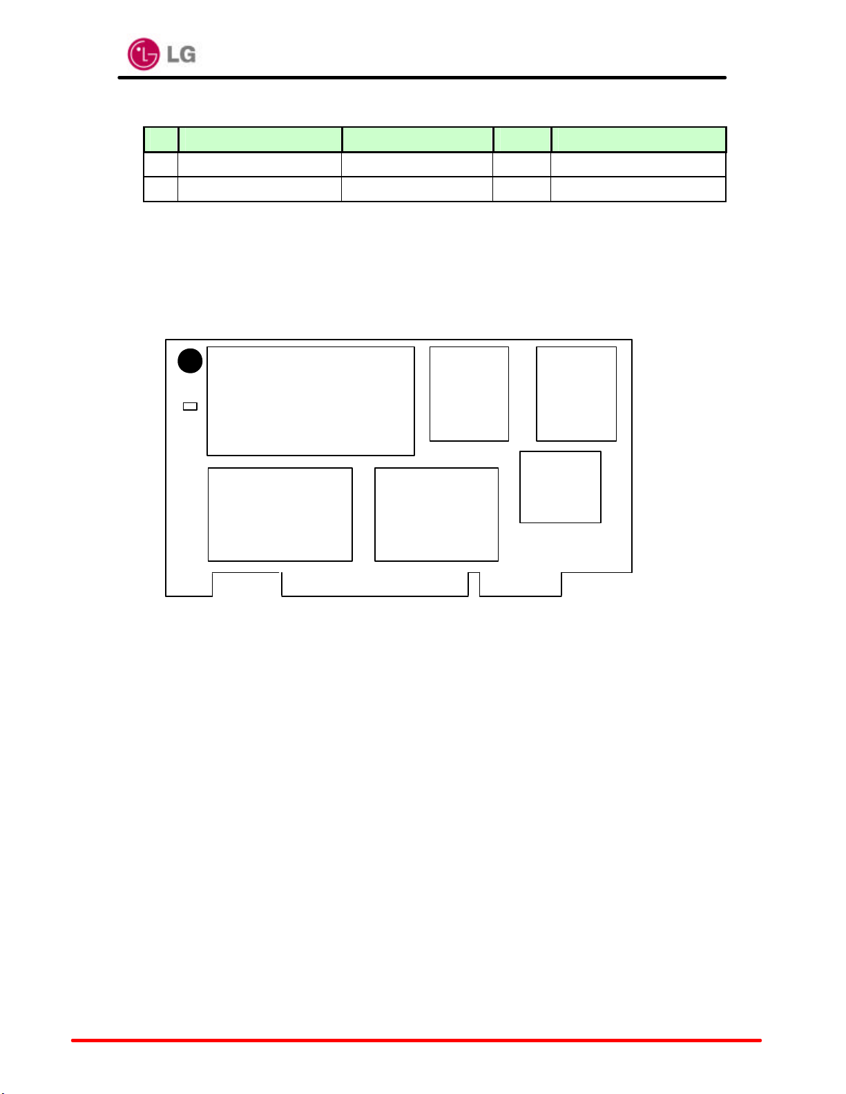
3.1 Block Layout
3.2 PCB Profile
lPCB Material : RCC & FR-4
lPCB Layer : 6 Layer Impedance Board
lPCB Size : 90.0mm(H) X 147.0mm(W) X 1.6mm(T)
Memory
Block
MAC
PCI
Controller
Power Supply
Block

LG GoldStream
11 of 11
4. Block Diagram

LG GoldStream
5. Circuit Diagram
Refer to attached files


LG GoldStream
6. Component Layout
6.1 Top Side (Component Layer)

LG GoldStream
6.2 Bottom Side (Solder Layer)

LG GoldStream
6.3 Component Layer

LG GoldStream
7. Part List
Refer to attached file

LG GoldStream
8. Photographs

LG GoldStream
9. Instruction Manual
Table of contents